Table of Contents
Advertisement
Quick Links
AN11022
CLRC663 Quickstart Guide
Rev. 1.1 — 12 July 2012
205911
Document information
Info
Content
Keywords
RC663, Reader IC, Power Supply, Interfacing RC663, RC663 Quick start
up, Functional description, Register settings
Abstract
This document describes the required basic circuitry to operate the
RC663 and it also describes how to set up first communication using the
RC663 Design-In Board (Demo Board V 3_0)
Application note
COMPANY PUBLIC
Advertisement
Table of Contents

Related Manuals for NXP Semiconductors I2C Bus AN11022


Summary of Contents for NXP Semiconductors I2C Bus AN11022
- Page 1 AN11022 CLRC663 Quickstart Guide Rev. 1.1 — 12 July 2012 Application note 205911 COMPANY PUBLIC Document information Info Content Keywords RC663, Reader IC, Power Supply, Interfacing RC663, RC663 Quick start up, Functional description, Register settings Abstract This document describes the required basic circuitry to operate the RC663 and it also describes how to set up first communication using the RC663 Design-In Board (Demo Board V 3_0)
- Page 2 AN11022 NXP Semiconductors CLRC663 Quickstart Guide Revision history Date Description 20120712 Some Figures updated because of quality reasons, Section Licenses updated 20120216 Initial release Contact information For more information, please visit: http://www.nxp.com For sales office addresses, please send an email to: salesaddresses@nxp.com...
-
Page 3: Introduction
AN11022 NXP Semiconductors CLRC663 Quickstart Guide 1. Introduction This document describes the basic requirements to power up the reader IC. This application note does not replace the CLRC663 datasheet. Please refer to the datasheet to read more information on each chapter. This document also gives an overview of the RC663 evaluation reader board and describes the function and first steps of using the board and the RC663. -
Page 4: Fig 1. Basic Wiring Diagram
AN11022 NXP Semiconductors CLRC663 Quickstart Guide 2.1 Basic wiring The basic wiring diagram can be found in Fig 1. The matching procedure of the antenna can be found in the application note AN11019 (Ref. 2). 470 nF 470 nF Fig 1. -
Page 5: Fig 2. Power Supply Diagram
AN11022 NXP Semiconductors CLRC663 Quickstart Guide AVDD V-Regulators 1.8V PDOWN Control DVDD TVDD TVSS Fig 2. Power supply diagram 2.3 Interface selection The CLRC663 supports direct interfacing of various hosts as the SPI, I C, I CL and serial UART interface type. The CLRC663 resets its interface and checks the current host interface type automatically having performed a Power-On or Hard Reset. -
Page 6: Fig 3. Crystal Connection
AN11022 NXP Semiconductors CLRC663 Quickstart Guide 2.4 Crystal oscillator The clock applied to the CLRC663 acts as a time basis for generation of the carrier sent out at TX, for the quadrature mixer I and Q clock generation, and for the coder and decoder of the synchronous system. -
Page 7: Hardware Design Of The Rc663 Evaluation Board ("Red Board")
AN11022 NXP Semiconductors CLRC663 Quickstart Guide 3. Hardware design of the RC663 evaluation board (“red board”) 3.1 Scope This part describes the functionality of the evaluation reader based on the RC663. It includes the functional and electrical specifications and gives the needed details to use this reader as a reference design. -
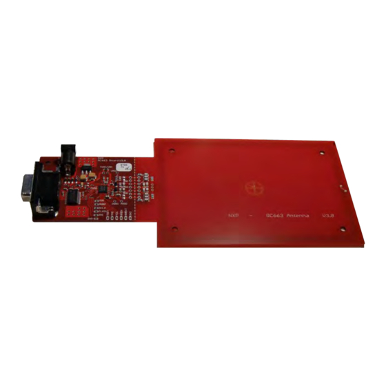
Page 8: Fig 4. Rc663 Board Version 3.0
AN11022 NXP Semiconductors CLRC663 Quickstart Guide 3.3 Functional description The RC663 evaluation reader is a contactless smartcard reader based on the RC663 reader IC. The Reader PCB is divided into 2 Parts, the general reader part and The Antenna and matching part: Table 3. -
Page 9: Pcb Marking And Major Improvements To Older Version
AN11022 NXP Semiconductors CLRC663 Quickstart Guide 3.4 PCB Marking and major improvements to older version There are two versions of the RC663 board version 2.0 and version 3.0 The latest version is: RC663 Board V3.0 The difference is shown below ( Fig 5) Improvements form V 2.0 to V 3.0:... -
Page 10: Fig 5. Nxp Rc663 Board V2.0 And 3.0
AN11022 NXP Semiconductors CLRC663 Quickstart Guide NXP RC663 Board V2.0 NXP RC663 Board V3.0 Fig 5. NXP RC663 Board V2.0 and 3.0 AN11022 All information provided in this document is subject to legal disclaimers. © NXP B.V. 2012. All rights reserved. -
Page 11: Fig 6. Power Supply Circuit
AN11022 NXP Semiconductors CLRC663 Quickstart Guide 3.5 Schematic description The following parts describe the RC663 evaluation reader board schematic, the part list, and the layout of the PCB completely in order to give the user the possibility to take the evaluation reader as a reference design for contactless smartcard reader integration. -
Page 12: Fig 7. Rs232 Interface And Transceiver
AN11022 NXP Semiconductors CLRC663 Quickstart Guide 3.6.2 RS232 Host interface Fig 7. RS232 interface and transceiver The DSUB-9 socket is used for a standard RS232 connection to the PC. For this interface the following values are assembled: Table 4. Used devices for RS232 interface... - Page 13 AN11022 NXP Semiconductors CLRC663 Quickstart Guide Table 5. DSUB-9 Pinning for RS232 Signal Voltage DCD (Data Carrier Detect) ± 3 – 12 V RD (Receive Data) ± 3 – 12 V TD (Transmit Data) ± 3 – 12 V DTR (Data Terminal Ready) ±...
-
Page 14: Microcontroller Interface Type
AN11022 NXP Semiconductors CLRC663 Quickstart Guide 3.6.3 Microcontroller interface type The CLRC663 supports direct interfacing of various hosts as the SPI, I2C, I2CL and serial UART interface type. The CLRC663 resets its interface and checks the current host interface type automatically having performed a Power-On or Hard Reset. The CLRC663 identifies the host interface by the means of the logic levels on the control pins after the Reset Phase. -
Page 15: Fig 8. Rc663 Schematic
AN11022 NXP Semiconductors CLRC663 Quickstart Guide 3.6.5 RC663 schematic This part shows a short overview of the RC336 schematic with all connections and also the oscillator part of the evaluation reader. Fig 8. RC663 Schematic Table 6. Used devices for RC663 Schematic including oscillator... -
Page 16: Fig 9. Antenna And Transceiver Circuit
AN11022 NXP Semiconductors CLRC663 Quickstart Guide 3.6.6 Antenna circuit The Transceiver circuit is divided into 3 Parts: the Antenna, Matching Circuit, and EMC Filter. The matching part of the transceiver circuit is responsible for the matching resistance of the whole Tx circuit. To tune your Antenna to the target resistance C1 and C2 have to be adjusted. -
Page 17: Fig 10. Schematic Of The Antenna And Transceiver Circuit
AN11022 NXP Semiconductors CLRC663 Quickstart Guide Fig 10. Schematic of the Antenna and Transceiver circuit Table 7. Used devices for RC663 Schematic including oscillator Device Value R7 / R8 4,7 Ω Damping Resistors for Q limitation 12 pF 12 pF... - Page 18 AN11022 NXP Semiconductors CLRC663 Quickstart Guide Device Value 68 pF 15 kΩ 15 kΩ n.A. n.A. Receiver 100 nF circuit 1 nF 1 nF 1 kΩ 1 kΩ AN11022 All information provided in this document is subject to legal disclaimers.
-
Page 19: Fig 11. Top Layer Rc663 Board
AN11022 NXP Semiconductors CLRC663 Quickstart Guide 3.7 PCB description and functionality 3.7.1 Top layer and placing Fig 11. Top layer RC663 board AN11022 All information provided in this document is subject to legal disclaimers. © NXP B.V. 2012. All rights reserved. -
Page 20: Fig 12. Parameter Selection Placement Top Layer
AN11022 NXP Semiconductors CLRC663 Quickstart Guide Fig 12. Parameter Selection Placement Top Layer AN11022 All information provided in this document is subject to legal disclaimers. © NXP B.V. 2012. All rights reserved. Application note Rev. 1.1 — 12 July 2012... -
Page 21: Fig 13. Bottom Layer Rc663 Board
AN11022 NXP Semiconductors CLRC663 Quickstart Guide 3.7.2 Bottom, middle layer and placing Fig 13. Bottom layer RC663 board AN11022 All information provided in this document is subject to legal disclaimers. © NXP B.V. 2012. All rights reserved. Application note Rev. 1.1 — 12 July 2012... -
Page 22: Fig 14. Placement Bottom Layer
AN11022 NXP Semiconductors CLRC663 Quickstart Guide Fig 14. Placement bottom Layer AN11022 All information provided in this document is subject to legal disclaimers. © NXP B.V. 2012. All rights reserved. Application note Rev. 1.1 — 12 July 2012 22 of 48... -
Page 23: Fig 15. Middle Layer Rc663 Board
AN11022 NXP Semiconductors CLRC663 Quickstart Guide Fig 15. Middle layer RC663 board AN11022 All information provided in this document is subject to legal disclaimers. © NXP B.V. 2012. All rights reserved. Application note Rev. 1.1 — 12 July 2012 23 of 48... -
Page 24: Fig 16. Pcb Antenna Section
AN11022 NXP Semiconductors CLRC663 Quickstart Guide 3.7.3 PCB antenna section Refer to section Receiver RxN Damping Matching resistors circuit EMC Filter Receiver RxP Fig 16. PCB antenna section The matching circuit and the antenna with damping resistor part of the RC663 board can be separated by cutting the board along the white dashed line on the top side of the board. -
Page 25: Register Settings For Different Modes And Features
AN11022 NXP Semiconductors CLRC663 Quickstart Guide To connect a different antenna, J1-J7 can be used (after cutting the board). Table 8. Antenna section connector Connector via Signal 4. Register Settings for different modes and features 4.1 EMD suppression The EMD suppression feature is only for ISO 14443 use cases. -
Page 26: Load Protocol Command
AN11022 NXP Semiconductors CLRC663 Quickstart Guide 4.2 Load Protocol command The Load Protocol command reads data from the internal EEPROM and initializes the CLRC663 registers needed for a Protocol change. The command reads out the EEPROM (RX and TX protected area) and copies the values from the RX- and TX protected area into the Registers. - Page 27 AN11022 NXP Semiconductors CLRC663 Quickstart Guide Example for using the load protocol with the CLRC663 PcSerial.3.6.exe.: CHB 115200 Terminate any running command. Flush_FiFo SR 00 00 SR 02 b0 // Clear all IRQ 0,1 flags SR 06 7f SR 07 7f //>...
-
Page 28: Iso/Iec 14443 Type A Recommended Register Settings
AN11022 NXP Semiconductors CLRC663 Quickstart Guide SR 09 00 //> Flush Fifo. Read Error Reg SR 02 B0 GR 0A 4.3 ISO/IEC 14443 Type A recommended register settings The following section gives an overview of the recommended register settings for ISO/IEC 14443 Type A communication, with different Antenna sizes (ID1, ID2, ID3). -
Page 29: Iso/Iec 14443 Type A For Id1 Sized Antenna
AN11022 NXP Semiconductors CLRC663 Quickstart Guide 4.3.1 ISO/IEC 14443 Type A for ID1 sized antenna Table 11. Register settings Type A ID1 sized antenna Reg descr 106 kbit/s 212 kbit/s 424 kbit/s 848 kbit/s DrvMode_Reg 0x8A 0x8E 0x8E 0x8F TxAmp_Reg... -
Page 30: Iso/Iec 14443 Type A For Id2 Sized Antenna
AN11022 NXP Semiconductors CLRC663 Quickstart Guide 4.3.2 ISO/IEC 14443 Type A for ID2 sized antenna Table 12. Register settings Type A ID2 sized antenna Reg descr 106 kbit/s 212 kbit/s 424 kbit/s 848 kbit/s DrvMode_Reg 0x8A 0x8E 0x8E 0x8F TxAmp_Reg... -
Page 31: Iso/Iec 14443 Type A For Id3 Sized Antenna
AN11022 NXP Semiconductors CLRC663 Quickstart Guide 4.3.3 ISO/IEC 14443 Type A for ID3 sized antenna Table 13. Register settings Type A ID3 sized antenna Reg descr 106 kbit/s 212 kbit/s 424 kbit/s 848 kbit/s DrvMode_Reg 0x8E 0x8E 0x8E 0x8F TxAmp_Reg... -
Page 32: Iso/Iec 14443 Type B Recommended Register Settings
AN11022 NXP Semiconductors CLRC663 Quickstart Guide 4.4 ISO/IEC 14443 Type B recommended register settings The following section gives an overview of the recommended register settings for ISO/IEC 14443 Type B communication, with different Antenna sizes (ID1, ID2, ID3). 4.4.1 Type B for ID1 sized antenna Table 14. -
Page 33: Type B For Id2 Sized Antenna
AN11022 NXP Semiconductors CLRC663 Quickstart Guide 4.4.2 Type B for ID2 sized antenna Table 15. Register settings Type B ID2 sized antenna Reg descr 106 kbit/s 212 kbit/s 424 kbit/s 848 kbit/s DrvMode_Reg 0x8F 0x8F 0x8F 0x8F TxAmp_Reg 0xCC 0xCC... -
Page 34: Type B For Id3 Sized Antenna
AN11022 NXP Semiconductors CLRC663 Quickstart Guide 4.4.3 Type B for ID3 sized antenna Table 16. Register settings Type B ID3 sized antenna Reg descr 106 kbit/s 212 kbit/s 424 kbit/s 848 kbit/s DrvMode_Reg 0x8F 0x8F 0x8F 0x8F TxAmp_Reg 0x0C 0x0C... -
Page 35: Felica Recommended Register Settings
AN11022 NXP Semiconductors CLRC663 Quickstart Guide 4.5 FeliCa recommended register settings The following section gives an overview of the recommended register settings for FeliCa communication, with different antenna sizes (ID1, ID2, ID3). 4.5.1 FeliCa for ID1 sized antenna Table 17. Register settings FeliCa ID1 sized antenna... -
Page 36: Felica For Id2 Sized Antenna
AN11022 NXP Semiconductors CLRC663 Quickstart Guide 4.5.2 FeliCa for ID2 sized antenna Table 18. Register settings FeliCa ID2 sized antenna Reg descr 212 kbit/s 424 kbit/s DrvMode_Reg 0x8F 0x8F TxAmp_Reg 0x17 0x17 DrvCon_Reg 0x01 0x01 TxI_Reg 0x06 0x06 TXCrcCon 0x09... -
Page 37: Felica For Id3 Sized Antenna
AN11022 NXP Semiconductors CLRC663 Quickstart Guide 4.5.3 FeliCa for ID3 sized antenna Table 19. Register settings FeliCa ID3 sized antenna Reg descr 212 kbit/s 424 kbit/s DrvMode_Reg 0x8F 0x8F TxAmp_Reg 0x17 0x17 DrvCon_Reg 0x01 0x01 TxI_Reg 0x0A 0x0A TXCrcCon 0x09... -
Page 38: Iso/Iec 15693 Recommended Register Settings
AN11022 NXP Semiconductors CLRC663 Quickstart Guide 4.6 ISO/IEC 15693 recommended register settings The following section gives an overview of the recommended register settings for ISO/IEC 15693 communication, with different Antenna sizes (ID1, ID2, ID3). 4.6.1 ISO/IEC 15693 for ID1 sized antenna Table 20. -
Page 39: Iso/Iec 15693 For Id2 Sized Antenna
AN11022 NXP Semiconductors CLRC663 Quickstart Guide 4.6.2 ISO/IEC 15693 for ID2 sized antenna Table 21. Register settings I-Code ID2 sized antenna SLI ¼ SLI ¼ SLI 1/256 Reg descr SSC26 SSC52 DrvMode_Reg 0x8F 0x8F 0x8E TxAmp_Reg 0x10 0x10 0x10 DrvCon_Reg... -
Page 40: Iso/Iec 15693 For Id3 Sized Antenna
AN11022 NXP Semiconductors CLRC663 Quickstart Guide 4.6.3 ISO/IEC 15693 for ID3 sized antenna Table 22. Register settings I-Code ID3 sized antenna SLI ¼ SLI ¼ SLI 1/256 Reg descr SSC26 SSC52 DrvMode_Reg 0x8F 0x8F 0x8E TxAmp_Reg 0x17 0x17 0x17 DrvCon_Reg... -
Page 41: Iso18000-3 Mode3 Recommended Register Settings
AN11022 NXP Semiconductors CLRC663 Quickstart Guide 4.7 ISO18000-3 Mode3 recommended register settings 4.7.1 ISO18000-3 Mode3 ID1 sized antenna Table 23. ISO18000-3 Mode3 ID1 sized antenna EPC V2 EPC V2 EPC V2 EPC V2 Reg descr 2/424 4/424 2/848 4/848 DrvMode_Reg... -
Page 42: Iso18000-3 Mode3 Id2 Sized Antenna
AN11022 NXP Semiconductors CLRC663 Quickstart Guide 4.7.2 ISO18000-3 Mode3 ID2 sized antenna Table 24. ISO18000-3 Mode3 ID2 sized antenna EPC V2 EPC V2 EPC V2 EPC V2 Reg descr 2/424 4/424 2/848 4/848 DrvMode_Reg 0x8F 0x8F 0x8F 0x8F TxAmp_Reg 0x10... -
Page 43: Iso18000-3 Mode3 Id3 Sized Antenna
AN11022 NXP Semiconductors CLRC663 Quickstart Guide 4.7.3 ISO18000-3 Mode3 ID3 sized antenna Table 25. ISO18000-3 Mode3 ID3 sized antenna EPC V2 EPC V2 EPC V2 EPC V2 Reg descr 2/424 4/424 2/848 4/848 DrvMode_Reg 0x8F 0x8F 0x8F 0x8F TxAmp_Reg 0x17... -
Page 44: References
AN11022 NXP Semiconductors CLRC663 Quickstart Guide 5. References [1] Product Data Sheet; CLRC663 Contactless reader IC (Doc. Nr.:1711xx) [2] Application note; AN11019 CLRC663 Antenna Design Guide (Doc. Nr.:2058xx) [3] Application note; AN11116 (“Using the RS232 serial evaluation boards on a USB port”), (Doc. -
Page 45: Legal Information
Purchase of NXP ICs with NFC technology Customers are responsible for the design and operation of their applications Purchase of an NXP Semiconductors IC that complies with one of the Near and products using NXP Semiconductors products, and NXP Field Communication (NFC) standards ISO/IEC 18092 and ISO/IEC 21481... -
Page 46: Table Of Contents
AN11022 NXP Semiconductors CLRC663 Quickstart Guide 7. List of figures Fig 1. Basic wiring diagram ......... 4 Fig 2. Power supply diagram ........5 Fig 3. Crystal connection ..........6 Fig 4. RC663 board version 3.0 ........8 Fig 5. -
Page 47: List Of Tables
AN11022 NXP Semiconductors CLRC663 Quickstart Guide 8. List of tables Table 1. Connection Scheme for detecting the different Interface Types ..........5 Table 2. Crystal requirements recommendations ... 6 Table 3. PCB sections ............ 8 Table 4. Used devices for RS232 interface ....12 Table 5. -
Page 48: Contents
AN11022 NXP Semiconductors CLRC663 Quickstart Guide 9. Contents 4.6.1 ISO/IEC 15693 for ID1 sized antenna ....38 Introduction ............3 4.6.2 ISO/IEC 15693 for ID2 sized antenna ....39 General description of the RC663 ...... 3 4.6.3 ISO/IEC 15693 for ID3 sized antenna ....40 Basic wiring ............
Need help?
Do you have a question about the I2C Bus AN11022 and is the answer not in the manual?
Questions and answers