Table of Contents
Advertisement
Quick Links
1. General description
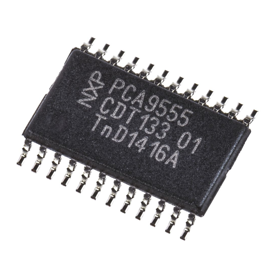
The PCA9555 is a 24-pin CMOS device that provides 16 bits of General Purpose parallel
Input/Output (GPIO) expansion for I
enhance the NXP Semiconductors family of I
include higher drive capability, 5 V I/O tolerance, lower supply current, individual I/O
configuration, and smaller packaging. I/O expanders provide a simple solution when
additional I/O is needed for ACPI power switches, sensors, push buttons, LEDs, fans, etc.
The PCA9555 consists of two 8-bit Configuration (Input or Output selection); Input, Output
and Polarity Inversion (active HIGH or active LOW operation) registers. The system
master can enable the I/Os as either inputs or outputs by writing to the I/O configuration
bits. The data for each Input or Output is kept in the corresponding Input or Output
register. The polarity of the read register can be inverted with the Polarity Inversion
register. All registers can be read by the system master. Although pin-to-pin and I
address compatible with the PCF8575, software changes are required due to the
enhancements, and are discussed in Application Note AN469.
The PCA9555 open-drain interrupt output is activated when any input state differs from its
corresponding input port register state and is used to indicate to the system master that
an input state has changed. The power-on reset sets the registers to their default values
and initializes the device state machine.
Three hardware pins (A0, A1, A2) vary the fixed I
devices to share the same I
the same as the PCA9554, allowing up to eight of these devices in any combination to
share the same I
2. Features and benefits
PCA9555
2
16-bit I
C-bus and SMBus I/O port with interrupt
Rev. 10 — 8 November 2017
2
C-bus/SMBus.
Operating power supply voltage range of 2.3 V to 5.5 V
5 V tolerant I/Os
Polarity Inversion register
Active LOW interrupt output
Low standby current
Noise filter on SCL/SDA inputs
No glitch on power-up
Internal power-on reset
16 I/O pins which default to 16 inputs
0 Hz to 400 kHz clock frequency
ESD protection exceeds 2000 V HBM per JESD22-A114, 200 V MM per
JESD22-A115, and 1000 V CDM per JESD22-C101
2
C-bus/SMBus applications and was developed to
2
C-bus I/O expanders. The improvements
2
C-bus address and allow up to eight
2
C-bus/SMBus. The fixed I
Product data sheet
2
C-bus address of the PCA9555 is
2
C-bus
Advertisement
Table of Contents

Subscribe to Our Youtube Channel
Related Manuals for NXP Semiconductors PCA9555


Summary of Contents for NXP Semiconductors PCA9555
-
Page 1: General Description
Rev. 10 — 8 November 2017 Product data sheet 1. General description The PCA9555 is a 24-pin CMOS device that provides 16 bits of General Purpose parallel Input/Output (GPIO) expansion for I C-bus/SMBus applications and was developed to enhance the NXP Semiconductors family of I C-bus I/O expanders. -
Page 2: Ordering Information
HWQFN24 REEL 13" Q1/T1 *STANDARD 6000 MARK SMD PCA9555 All information provided in this document is subject to legal disclaimers. © NXP Semiconductors N.V. 2017. All rights reserved. Product data sheet Rev. 10 — 8 November 2017 2 of 34... -
Page 3: Block Diagram
IO1_0 002aac698 Fig 2. Pin configuration for SO24 PCA9555 All information provided in this document is subject to legal disclaimers. © NXP Semiconductors N.V. 2017. All rights reserved. Product data sheet Rev. 10 — 8 November 2017 3 of 34... - Page 4 Pin configuration for HVQFN24 Fig 6. Pin configuration for HWQFN24 PCA9555 All information provided in this document is subject to legal disclaimers. © NXP Semiconductors N.V. 2017. All rights reserved. Product data sheet Rev. 10 — 8 November 2017 4 of 34...
-
Page 5: Pin Description
PCB in the thermal pad region. PCA9555 All information provided in this document is subject to legal disclaimers. © NXP Semiconductors N.V. 2017. All rights reserved. Product data sheet Rev. 10 — 8 November 2017... -
Page 6: Functional Description
Polarity Inversion port 1 Configuration port 0 Configuration port 1 PCA9555 All information provided in this document is subject to legal disclaimers. © NXP Semiconductors N.V. 2017. All rights reserved. Product data sheet Rev. 10 — 8 November 2017 6 of 34... -
Page 7: Registers 0 And 1: Input Port Registers
N1.6 N1.5 N1.4 N1.3 N1.2 N1.1 N1.0 Default PCA9555 All information provided in this document is subject to legal disclaimers. © NXP Semiconductors N.V. 2017. All rights reserved. Product data sheet Rev. 10 — 8 November 2017 7 of 34... -
Page 8: Registers 6 And 7: Configuration Registers
V . At that point, the reset condition is released and the PCA9555 registers and SMBus state machine will initialize to their default states. The power-on reset typically completes the reset and enables the part by the time the power supply is above V . -
Page 9: Bus Transactions
Simplified schematic of I/Os 6.5 Bus transactions 6.5.1 Writing to the port registers Data is transmitted to the PCA9555 by sending the device address and setting the least significant bit to a logic 0 (see Figure 7 “PCA9555 device address”). The command byte is sent after the address and determines which register will receive the data following the command byte. -
Page 10: Pca9555
xxxxxxxxxxxxxxxxxxxxx xxxxxxxxxxxxxxxxxxxxxxxxxx xxxxxxx x x x xxxxxxxxxxxxxxxxxxxxxxxxxxxxxx xxxxxxxxxxxxxxxxxxx xx xx xxxxx xxxxxxxxxxxxxxxxxxxxxxxxxxx xxxxxxxxxxxxxxxxxxx xxxxxx xxxxxxxxxxxxxxxxxxxxxxxxxxxxxxxxxxx xxxxxxxxxxxx x x xxxxxxxxxxxxxxxxxxxxx xxxxxxxxxxxxxxxxxxxxxxxxxxxxxx xxxxx xxxxxxxxxxxxxxxxxxxxxxxxxxxxxxxxxxxxxxxxxxxxxxxxxx xxxxxxxx xxxxxxxxxxxxxxxxxxxxxxxxx xxxxxxxxxxxxxxxxxxxx xxx slave address command byte data to port 0 data to port 1 0 A2 A1 A0 0 DATA 0 DATA 1 START condition... -
Page 11: Reading The Port Registers
C-bus and SMBus I/O port with interrupt 6.5.2 Reading the port registers In order to read data from the PCA9555, the bus master must first send the PCA9555 address with the least significant bit set to a logic 0 (see Figure 7 “PCA9555 device... - Page 12 xxxxxxxxxxxxxxxxxxxxx xxxxxxxxxxxxxxxxxxxxxxxxxx xxxxxxx x x x xxxxxxxxxxxxxxxxxxxxxxxxxxxxxx xxxxxxxxxxxxxxxxxxx xx xx xxxxx xxxxxxxxxxxxxxxxxxxxxxxxxxx xxxxxxxxxxxxxxxxxxx xxxxxx xxxxxxxxxxxxxxxxxxxxxxxxxxxxxxxxxxx xxxxxxxxxxxx x x xxxxxxxxxxxxxxxxxxxxx xxxxxxxxxxxxxxxxxxxxxxxxxxxxxx xxxxx xxxxxxxxxxxxxxxxxxxxxxxxxxxxxxxxxxxxxxxxxxxxxxxxxx xxxxxxxx xxxxxxxxxxxxxxxxxxxxxxxxx xxxxxxxxxxxxxxxxxxxx xxx data into port 0 data into port 1 v(INT_N) rst(INT_N) STOP condition slave address I0.x I1.x I0.x...
- Page 13 xxxxxxxxxxxxxxxxxxxxx xxxxxxxxxxxxxxxxxxxxxxxxxx xxxxxxx x x x xxxxxxxxxxxxxxxxxxxxxxxxxxxxxx xxxxxxxxxxxxxxxxxxx xx xx xxxxx xxxxxxxxxxxxxxxxxxxxxxxxxxx xxxxxxxxxxxxxxxxxxx xxxxxx xxxxxxxxxxxxxxxxxxxxxxxxxxxxxxxxxxx xxxxxxxxxxxx x x xxxxxxxxxxxxxxxxxxxxx xxxxxxxxxxxxxxxxxxxxxxxxxxxxxx xxxxx xxxxxxxxxxxxxxxxxxxxxxxxxxxxxxxxxxxxxxxxxxxxxxxxxx xxxxxxxx xxxxxxxxxxxxxxxxxxxxxxxxx xxxxxxxxxxxxxxxxxxxx xxx data into port 0 DATA 00 DATA 01 DATA 02 DATA 03 h(D) su(D) data into port 1 DATA 10 DATA 11...
-
Page 14: Interrupt Output
Fig 15. Definition of START and STOP conditions PCA9555 All information provided in this document is subject to legal disclaimers. © NXP Semiconductors N.V. 2017. All rights reserved. Product data sheet Rev. 10 — 8 November 2017 14 of 34... -
Page 15: System Configuration
Fig 17. Acknowledgement on the I C-bus PCA9555 All information provided in this document is subject to legal disclaimers. © NXP Semiconductors N.V. 2017. All rights reserved. Product data sheet Rev. 10 — 8 November 2017 15 of 34... -
Page 16: Application Design-In Information
IO0_6, IO0_7, and IO1_0 to IO1_7 configured as inputs. Fig 18. Typical application PCA9555 All information provided in this document is subject to legal disclaimers. © NXP Semiconductors N.V. 2017. All rights reserved. Product data sheet Rev. 10 — 8 November 2017 16 of 34... -
Page 17: Limiting Values
C maximum junction j(max) temperature PCA9555 All information provided in this document is subject to legal disclaimers. © NXP Semiconductors N.V. 2017. All rights reserved. Product data sheet Rev. 10 — 8 November 2017 17 of 34... -
Page 18: Static Characteristics
0.2 V for at least 5 s in order to reset part. PCA9555 All information provided in this document is subject to legal disclaimers. © NXP Semiconductors N.V. 2017. All rights reserved. Product data sheet Rev. 10 — 8 November 2017... - Page 19 Fig 21. I versus number of I/Os held LOW PCA9555 All information provided in this document is subject to legal disclaimers. © NXP Semiconductors N.V. 2017. All rights reserved. Product data sheet Rev. 10 — 8 November 2017 19 of 34...
-
Page 20: Dynamic Characteristics
= total capacitance of one bus line in pF. PCA9555 All information provided in this document is subject to legal disclaimers. © NXP Semiconductors N.V. 2017. All rights reserved. Product data sheet Rev. 10 — 8 November 2017 20 of 34... -
Page 21: Test Information
500 Ω 50 pF 002aac226 Fig 24. Load circuit PCA9555 All information provided in this document is subject to legal disclaimers. © NXP Semiconductors N.V. 2017. All rights reserved. Product data sheet Rev. 10 — 8 November 2017 21 of 34... -
Page 22: Package Outline
MS-013 03-02-19 Fig 25. Package outline SOT137-1 (SO24) PCA9555 All information provided in this document is subject to legal disclaimers. © NXP Semiconductors N.V. 2017. All rights reserved. Product data sheet Rev. 10 — 8 November 2017 22 of 34... - Page 23 MO-150 03-02-19 Fig 26. Package outline SOT340-1 (SSOP24) PCA9555 All information provided in this document is subject to legal disclaimers. © NXP Semiconductors N.V. 2017. All rights reserved. Product data sheet Rev. 10 — 8 November 2017 23 of 34...
- Page 24 MO-153 03-02-19 Fig 27. Package outline SOT355-1 (TSSOP24) PCA9555 All information provided in this document is subject to legal disclaimers. © NXP Semiconductors N.V. 2017. All rights reserved. Product data sheet Rev. 10 — 8 November 2017 24 of 34...
- Page 25 - - - 02-10-22 Fig 28. Package outline SOT616-1 (HVQFN24) PCA9555 All information provided in this document is subject to legal disclaimers. © NXP Semiconductors N.V. 2017. All rights reserved. Product data sheet Rev. 10 — 8 November 2017 25 of 34...
- Page 26 MO-220 07-03-03 Fig 29. Package outline SOT994-1 (HWQFN24) PCA9555 All information provided in this document is subject to legal disclaimers. © NXP Semiconductors N.V. 2017. All rights reserved. Product data sheet Rev. 10 — 8 November 2017 26 of 34...
-
Page 27: Handling Information
15.3 Wave soldering Key characteristics in wave soldering are: PCA9555 All information provided in this document is subject to legal disclaimers. © NXP Semiconductors N.V. 2017. All rights reserved. Product data sheet Rev. 10 — 8 November 2017 27 of 34... -
Page 28: Reflow Soldering
Studies have shown that small packages reach higher temperatures during reflow soldering, see Figure PCA9555 All information provided in this document is subject to legal disclaimers. © NXP Semiconductors N.V. 2017. All rights reserved. Product data sheet Rev. 10 — 8 November 2017 28 of 34... -
Page 29: Soldering Of Through-Hole Mount Packages
300 C and 400 C, contact may be up to 5 seconds. PCA9555 All information provided in this document is subject to legal disclaimers. © NXP Semiconductors N.V. 2017. All rights reserved. Product data sheet Rev. 10 — 8 November 2017... -
Page 30: Package Related Soldering Information
Field-Effect Transistor Most Significant Bit Least Significant Bit PCA9555 All information provided in this document is subject to legal disclaimers. © NXP Semiconductors N.V. 2017. All rights reserved. Product data sheet Rev. 10 — 8 November 2017 30 of 34... -
Page 31: Revision History
(9397 750 09818) PCA9555_1 20010507 Product data (9397 750 08343) PCA9555 All information provided in this document is subject to legal disclaimers. © NXP Semiconductors N.V. 2017. All rights reserved. Product data sheet Rev. 10 — 8 November 2017 31 of 34... -
Page 32: Legal Information
For detailed and full information see the relevant full data specified use without further testing or modification. sheet, which is available on request via the local NXP Semiconductors sales Customers are responsible for the design and operation of their applications office. -
Page 33: Trademarks
NXP Semiconductors’ specifications such use shall be solely at customer’s authorization from competent authorities. own risk, and (c) customer fully indemnifies NXP Semiconductors for any liability, damages or failed product claims resulting from customer design and Quick reference data — The Quick reference data is an extract of the use of the product for automotive applications beyond NXP Semiconductors’... -
Page 34: Table Of Contents
Package related soldering information ..30 Please be aware that important notices concerning this document and the product(s) described herein, have been included in section ‘Legal information’. © NXP Semiconductors N.V. 2017. All rights reserved. For more information, please visit: http://www.nxp.com For sales office addresses, please send an email to: salesaddresses@nxp.com...
Need help?
Do you have a question about the PCA9555 and is the answer not in the manual?
Questions and answers