
Related Manuals for Aaeon HSB-800I-A11


Summary of Contents for Aaeon HSB-800I-A11
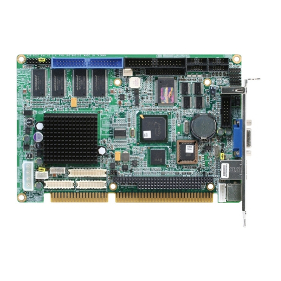
- Page 1 HSB-800I-A11 Half-Sized ISA SBC User’s Manual 1 Last Updated: January 7, 2021...
- Page 2 AAEON assumes no liabilities resulting from errors or omissions in this document, or from the use of the information contained herein. AAEON reserves the right to make changes in the product design without notice to its users.
- Page 3 Acknowledgement All other products’ name or trademarks are properties of their respective owners. Microsoft Windows is a registered trademark of Microsoft Corp. ⚫ AMD and AMD Geode™ are registered trademarks of Advanced Micro Devices, ⚫ Inc. ITE is a trademark of Integrated Technology Express, Inc. ⚫...
- Page 4 Packing List Before setting up your product, please make sure the following items have been shipped: Item Description Quantity HSB-800I-A11 Half-Sized Board Flat Cable.9P/DB9P MALE&25P DB25P FEMALE.10P 1701260307 2mm&26P 2mm/IDC NO FOLD.30cm.W/BKT Cable.40P 2.54mm IDC W/Nose W/Fold.40P 2.54mm 1701400453 IDC W/Nose W/Fold.45cm.Blue ATA-100 1700060192 Cable.6P-6P-6P.19cm.IVORY PS2/KB&Mouse...
- Page 5 (if any), its specifications, dimensions, jumper/connector settings/definitions, and driver installation instructions (if any), to facilitate users in setting up their product. Users may refer to the product page at AAEON.com for the latest version of this document. Preface...
- Page 6 Safety Precautions Please read the following safety instructions carefully. It is advised that you keep this manual for future references All cautions and warnings on the device should be noted. Make sure the power source matches the power rating of the device. Position the power cord so that people cannot step on it.
- Page 7 If any of the following situations arises, please the contact our service personnel: Damaged power cord or plug Liquid intrusion to the device iii. Exposure to moisture Device is not working as expected or in a manner as described in this manual The device is dropped or damaged Any obvious signs of damage displayed on the device...
- Page 8 FCC Statement This device complies with Part 15 FCC Rules. Operation is subject to the following two conditions: (1) this device may not cause harmful interference, and (2) this device must accept any interference received including interference that may cause undesired operation.
- Page 9 China RoHS Requirements (CN) 产品中有毒有害物质或元素名称及含量 AAEON Main Board/ Daughter Board/ Backplane 有毒有害物质或元素 部件名称 铅 汞 镉 六价铬 多溴联苯 多溴二苯醚 (Pb) (Hg) (Cd) (Cr(VI)) (PBB) (PBDE) 印刷电路板 ○ ○ ○ ○ ○ ○ 及其电子组件 外部信号 ○ ○ ○ ○ ○ ○...
- Page 10 China RoHS Requirement (EN) Poisonous or Hazardous Substances or Elements in Products AAEON Main Board/ Daughter Board/ Backplane Poisonous or Hazardous Substances or Elements Hexavalent Polybrominated Polybrominated Component Lead Mercury Cadmium Chromium Biphenyls Diphenyl Ethers (Pb) (Hg) (Cd) (Cr(VI)) (PBB) (PBDE) PCB &...
-
Page 11: Table Of Contents
Table of Contents Chapter 1 - Product Specifications..................1 Specifications ......................2 Chapter 2 – Hardware Information ..................4 Dimensions ....................... 5 Jumpers and Connectors ..................6 List of Jumpers and Switches ................7 2.3.1 CFD Voltage 3.3V/ 5V Selection (JP1) ............7 2.3.2 Clear CMOS (JP2) .................. - Page 12 2.4.15 IrDA Connector (IR1) .................. 17 2.4.16 LPT Port Connector (LPT1) ................ 17 2.4.17 USB2.0 Header (USB1/ USB2/ USB3) ............18 Function Block Diagram ..................19 Chapter 3 - Award BIOS Setup .................... 20 System Test and Initialization ................21 Award BIOS Setup ....................
-
Page 13: Chapter 1 - Product Specifications
Chapter 1 Chapter 1 - Product Specifications... -
Page 14: Specifications
Specifications System Form Factor PICMG 1.0 Half-Size Pure ISA CPU Card Bus Interface AMD Geode™ LX 800 Memory Type Onboard 128 MB DDR 400 Chipset AMD Geode™ CS 5536 BIOS Award Plug & Play FWH BIOS – 8MB ROM Wake on LAN Watchdog Timer 255 Levels Power Requirement... - Page 15 Display VGA/LCD Controller AMD Geode™ LX 800 Video Output 1600 x 1200@32bpp at 100 MHz for VGA 1600 x 1200@24bpp for LCD Backlight Inverter Supply 5V, 12V Ethernet 10/100 Mbps LAN x1 or 10/100/1000 Mbps LAN x1 (optional) Audio AC97 Codec USB Port USB2.0 x 4 Serial Port...
-
Page 16: Chapter 2 - Hardware Information
Chapter 2 Chapter 2 – Hardware Information... -
Page 17: Dimensions
Dimensions 185.00 15.20 8.60 Chapter 2 – Hardware Information... -
Page 18: Jumpers And Connectors
Jumpers and Connectors Component Side Solder Side Chapter 2 – Hardware Information... -
Page 19: List Of Jumpers And Switches
List of Jumpers and Switches Please refer to the table below for all of the board’s jumpers that you can configure for your application Label Function CFD Voltage 3.3V/ 5V Selection Clear CMOS AT/ATX Power Type Selection LCD Clock and Power Selection Inverter Voltage Selection 2.3.1 CFD Voltage 3.3V/ 5V Selection (JP1) -
Page 20: At/Atx Power Type Selection (Jp3)
2.3.3 AT/ATX Power Type Selection (JP3) Setting Function 1-2 Closed ATX Power Supply (Default) 1-2 Open AT Power Supply Note: Only AT Function without Backplanes. 2.3.4 LCD Clock and Power Selection (JP4) LCD Clock Selection Normal (Default) Inverse LCD Power Selection +5Vlcd +3Vlcd (Default) Note: To prevent damage to your system, do not use any other configuration for JP4... -
Page 21: List Of Connectors
List of Connectors Please refer to the table below for all of the board’s connectors that you can configure for your application Label Function CFD1 CompactFlash Type II Slot (always master) Digital I/O Fan Connector Audio Input/Output/CD-in/MIC LCD Inverter Power Connector TFT LCD Connector +5VSB Power Connector AT Power 5V, 12V Connector... -
Page 22: Digital I/O (Cn1)
Label Function LAN1 10/100 or 100/1000 Base-TX Ethernet Connector LPT1 LPT Port Connector USB1 USB2.0 Header USB2 USB2.0 Header USB3 USB2.0 Header USB4 USB2.0 Type A Connector VGA1 VGA Display Connector 2.4.1 Digital I/O (CN1) Signal Signal OUT0 OUT1 OUT2 OUT3 Chapter 2 –... -
Page 23: Fan Connector (Cn2)
2.4.2 Fan Connector (CN2) Signal Speed Sensor 2.4.3 Audio Input/ Output/ CD-in/ MIC (CN3) Signal Signal MIC_Vcc Audio Ground CD_GND LINE_IN L CD_L LINE_IN R CD_GND Audio Ground CD_R LINE_OUT L LINE_OUT R Audio Ground Audio Ground 2.4.4 LCD Inverter Power Connector (CN4) Signal 12V/ 5V VCON... -
Page 24: Tft Lcd Connector (Cn5)
2.4.5 TFT LCD Connector (CN5) For 24-bit TFT LCD Signal Signal +5VLCD +5VLCD +3.3VLCD +3.3VLCD BKL_EN LCD_CLK LCD_VS LCD_DE LCD_HS For 18-bit TFT LCD Signal Signal +5VLCD +5VLCD Chapter 2 – Hardware Information... -
Page 25: 5Vsb Power Connector (Cn6)
For 18-bit TFT LCD Signal Signal +3.3VLCD +3.3VLCD BKL_EN LCD_CLK LCD_VS LCD_DE LCD_HS 2.4.6 +5VSB Power Connector (CN6) Signal PS_ON# +5VSB Chapter 2 – Hardware Information... -
Page 26: At Power 5V, 12V Connector (Cn7)
2.4.7 AT Power 5V, 12V Connector (CN7) Signal +12V 2.4.8 LVDS Connector (CN9, 10) Signal Signal BKL_EN VLCD LVDS_CLK# LVDS_CLK VLCD TX0# TX1# TX2# TX3# Chapter 2 – Hardware Information... -
Page 27: Ps/2 Keyboard/Mouse Connector (Cn11)
Signal Signal VLCD 2.4.9 PS/2 Keyboard/Mouse Connector (CN11) Signal Signal KB_DATA MS-DATA KB_CLK MS_CLK 2.4.10 Internal Keyboard Connector (CN12) Signal KB_CLK KB_DATA Chapter 2 – Hardware Information... -
Page 28: Rs-232 Serial Port Header (Com1/ Com3/ Com4)
2.4.11 RS-232 Serial Port Header (COM1/ COM3/ COM4) Signal Signal 2.4.12 RS-232/422/485 Serial Port Header (COM2) Signal Signal DCD (422TXD-/485DATA-) 2 RXD (422RXD+) TXD (422TXD+/485DATA+) 4 DTR (422RXD-) 2.4.13 Front Panel Connector 1 (FP1) Signal Signal Power On Button (+) Reset Switch (+) Power On Button (-) Reset Switch (-) -
Page 29: Front Panel Connector 2 (Fp2)
2.4.14 Front Panel Connector 2 (FP2) Signal Signal External Speaker (+) Key Board Lock (+) Internal Buzzer (-) I2C Bus SMB Clock External Speaker (-) I2C Bus SMB Data 2.4.15 IrDA Connector (IR1) Signal Signal IRTX IRRX 2.4.16 LPT Port Connector (LPT1) Signal Signal #STROBE... -
Page 30: Usb2.0 Header (Usb1/ Usb2/ Usb3)
Signal Signal DATA6 DATA7 #ACK BUSY SELECT 2.4.17 USB2.0 Header (USB1/ USB2/ USB3) Signal USBD1- USBD1+ Chapter 2 – Hardware Information... -
Page 31: Function Block Diagram
Function Block Diagram Chapter 2 – Hardware Information... -
Page 32: Chapter 3 - Award Bios Setup
Chapter 3 Chapter 3 - Award BIOS Setup... -
Page 33: System Test And Initialization
The CMOS memory has lost power and the configuration information has been ⚫ erased. The HSB-800I-A11 CMOS memory uses a backup battery for data retention. The battery must be replaced if it runs out of power. Chapter 3 – AMI BIOS Setup... -
Page 34: Award Bios Setup
Award BIOS Setup The Award BIOS ROM has a built-in Setup program that allows users to modify the basic system configuration. This information is stored in the battery-backed CMOS RAM so it retains the Setup information when the power is turned off. To enter Setup, power on the system and press <Del>... - Page 35 Frequency/Voltage Control – Display (monitor) frequency and voltage control. Load Fail-Safe Defaults – Load BIOS default values for minimal/ stable performance for system operation. Load Optimized Defaults – Load BIOS default factory settings for optimal system performance. While Award has designed the custom BIOS to maximize performance, the factory has the right to change these defaults to meet their needs.
-
Page 36: Standard Cmos Features
Standard CMOS Features Date and Time Configuration The BIOS determines the day of the week from the other date information. This field is for information only. Press the left or right arrow key to move to the desired field (date, month, year). - Page 37 CHS: This allows the user to enter their own hardware values. Large: For drives that do not support LBA and have more than 1024 cylinders. LBA (Logical Block Addressing): During drive access, the IDE controller transforms the data address described by sector, head, and cylinder number into a physical block address, significantly improving data transfer rates for drives with greater than 1024 cylinders.
- Page 38 Video Halt On [Default: All, But Keyboard] During the power-on-self-test (POST), the computer stops if the BIOS detects a hardware error. You can tell BIOS to ignore certain errors during POST and continue the boot-up process. Memory [Default: AutoDetect] You cannot change any values in the Memory fields; they are only for your information. RAM is counted in kilobytes (KB: approximately one thousand bytes) and megabytes (MB: approximately one million bytes).
-
Page 39: Advanced Bios Features
Advanced BIOS Features CPU Feature [Default: Autodetect] Items will only enabled when current CPU is supported Thermal Monitor feature. Delay Prior to Thermal The Delay Prior To Thermal BIOS feature controls the [Default: 16 Min] activation of the Thermal Monitor's automatic mode. It allows you to determine when the Pentium 4's Thermal Monitor should be activated in automatic mode after the system boots. - Page 40 Use <↑> or <↓> to select a device, then press<+> to move it up, or <-> to move it down the list. Press <ESC> to exit this level of menu. CD-ROM Boot Priority [Default: Auto Detect] Select CD-ROM Boot Device Priority Virus Warning [Default: Disabled] When enabled, you receive a warning message if a program (specifically, a virus) attempts to write to the boot sector or the partition table of the hard disk drive.
- Page 41 Quick Power On Self Test [Default: Enabled] Select Enabled to reduce the amount of time required to run the power-on-self-test (POST). A quick POST skips certain steps. USB Floppy Disk Type [Default: Auto] Auto – By USB Device Floppy – Emulation to Floppy Mode HDD –...
- Page 42 Swap Floppy Drive [Default: Disabled] This field is effective only in systems with two floppy drives. Selecting enabled assigns physical drive B to logical drive A, and physical drive A to logical drive B. Boot Up Floppy Seek [Default: Enabled] When Enabled, the BIOS tests (seeks) floppy drives to determine whether they have 40 or 80 tracks.
- Page 43 Typematic Delay (Msec) [Default: 250] When the typematic rate setting is enabled, you can select a typematic delay (the delay before key strokes begin to repeat) of 250, 500, 750 or 1000 milliseconds. Security Option [Default: Setup] If you have set a password, select whether the password is required every time the System boots, or only when you enter Setup.
- Page 44 C8000-CBFFF Shadow [Default: Disabled] CC000-CFFFF Shadow [Default: Disabled] D0000-D3FFF Shadow [Default: Disabled] D4000-D7FFF Shadow [Default: Disabled] D8000-DBFFF Shadow [Default: Disabled] DC000-DFFFF Shadow [Default: Disabled] Software that resides in a read only memory (ROM) chip on a device is called firmware. The Award BIOS permits shadowing of firmware such as the system BIOS, video BIOS, and similar operating instructions that come with some expansion peripherals such as a SCSI adaptor.
-
Page 45: Advanced Chipset Features
Advanced Chipset Features DRAM Timing Selectable [Default: By SPD] When select to “By SPD”, the DRAM timing parameters are set according to DRAM SPD (Serial Presence Detect). When disabled, one can manually set the DRAM timing parameters through the sub items below. Set to “By SPD” if not sure. CAS Latency Time: [Default: 2] Controls the latency between the SDRAM Read command and the time data actually becomes available. - Page 46 System BIOS Cacheable [Default: Enabled] Selecting Enabled allows caching of the system BIOS ROM at F0000h-FFFFFh, resulting in better system performance. However, if any program writes to this memory area, a system error may result. Video BIOS Cacheable [Default: Disabled] Selecting Enabled allows caching of the video BIOS ROM at F0000h-FFFFFh, resulting in better video performance.
- Page 47 This option is used with various visual display peripherals. This function allows the end user to select the type of visual display peripheral they are incorporated with the AAEON single board computer. Panel Type [Default: Panel #1] When your display devices include LCD panel, you have to select the type of panel you are incorporating with your single board computer.
-
Page 48: Integrated Peripherals
Integrated Peripherals OnChip IDE Device OnChip Primary/ The integrated peripheral controller contains an IDE Secondary PCI IDE interface with support for two IDE channels. Select [Default: Enabled] Enabled to activate each channel separately. IDE Primary / Secondary The four IDE PIO (Programmable Input/Output) fields let Master / Slave PIO you set a PIO mode (0-1) for each of the two IDE devices [Default: Auto]... - Page 49 Serial ATA Port Mode Set up Serial ATA Port mode to Primary / Secondary, [Default: Primary Master] Master / Slave or SATA0 / SATA1 according to “Combined / Enhanced / SATA Only” selected on “OnChip Serial ATA” option. Onboard Device USB Controller Enable / Disable USB Controller.
- Page 50 SuperIO Device Note: Normally, the boards' I/O chips will occupy a certain portion of memory space. For each I/O device the computer provides an I/O address. The more devices attached the more address needed to organize the memory storage areas. If all the I/O devices were running through the same address, your devices would come to a near halt.
- Page 51 Use IR Pins Choose type of IR Pins. [Default: IR-Rx2Tx2] Onboard Parallel Port Select a logical LPT port address and corresponding [Default: 378/IRQ7] interrupt for the physical parallel port Parallel Port Mode Select Parallel port mode: [Default: SPP] SPP Using Parallel port as Standard Parallel Port. EPP Using Parallel port as Enhanced Parallel Port.
-
Page 52: Power Management Setup
Power Management Setup Power-Supply Type [Default: ATX] Choose System Power Supply Type. ATX or AT depends on the Hardware Specification. ACPI Function [Default: Enabled] Enable / Disable ACPI function. Power Management [Default: Min Saving] Select Max Saving mode or Min Saving mode or define desired Suspend Mode, HDD Power Down functions by User Define. - Page 53 Suspend Mode [Default: Disabled] Disable this function or select 1 min, 2 min, 4 min, 8 min, 12 min, 20min, 30 min, 40 min, 1 hour. HDD Power Down [Default: Disabled] Disable this function or select from 1 to 15 minutes. Soft-Off by PWR-BTTN [Default: Instant-Off] If you select "Instant -Off", pushing the on/off button will instantly shut down the system.
- Page 54 Enabled: Enable alarm function to power up system, if RTC Alarm Lead To Power On is Enabled. Date (of Month) Alarm: Everyday, 1~31 Time (hh: mm: ss) Alarm: (0~23): (0~59): (0~59) Chapter 3 – AMI BIOS Setup...
-
Page 55: Pnp/Pci Configurations
PnP/PCI Configurations PNP OS Installed [Default: No] Select Yes if the system operating environment is Plug and Play aware, for example Windows 95. Select No if you need the BIOS to configure non-boot devices. Reset Configuration Data [Default: Disabled] Normally, you leave this field disabled. Select enabled to reset Extended System Configuration Data (ESCD) when you exit Setup if you have installed a new add-on and the system reconfiguration has caused such a serious conflict that the operating system cannot boot. - Page 56 DMA Resources [Default: PCI/ISA PnP] When resources are controlled manually, assign each DMA channel a type, depending on the type of device using the DMA channel. Legacy ISA Devices compliant with the original PC AT bus specification, requiring a specific DMA channel PCI/ISA PnP Devices compliant with the Plug and Play standard, whether designed for PCI or ISA bus architecture.
-
Page 57: Pc Health Status
PC Health Status CPU Warning Temperature [Default: 70] Select the combination of lower and upper limits for the CPU temperature. If the CPU temperature extends beyond either limit, any warning mechanism programmed into your system will be activated. Shutdown Temperature [Default: Disable] The shutdown temperature for the computer shuts down by itself. - Page 58 +3.3V Current onboard 3.3V voltage value. Current onboard 5V voltage value. +12V Current onboard 12V voltage value. -12V Current onboard -12V voltage value. Current onboard -5V voltage value. VBAT(V) Current onboard VBAT voltage value. 5VSB(V) Current onboard 5VSB voltage value. Chapter 3 –...
-
Page 59: 3.10 Frequency/Voltage Control
3.10 Frequency/Voltage Control CPU Clock Ratio [Default: Auto detect] This option will not be shown or not be available if you are using a CPU with the locked ratio. This setup option will automatically assign by CPU detection. For C-Stepping P4: 8X, 10X~24X For Northwood CPU: 12X~24X The option will display "Locked"... -
Page 60: Chapter 4 - Drivers Installation
Chapter 4 Chapter 4 – Drivers Installation... -
Page 61: Drivers Download And Installation
Drivers Download and Installation Drivers for the HSB-800I-A11 can be downloaded from the product page on the AAEON website by following this link: https://www.aaeon.com/en/p/half-size-sbc-hsb-800i Download the driver(s) you need and follow the steps below, to install them. The downloadable drivers are executable installers. Simply double click each driver to run the installation wizard and follow the steps on your screen. -
Page 62: Appendix A - Watchdog Timer
Appendix A Appendix A - Watchdog Timer... -
Page 63: Programming The Watchdog Timer
Programming the Watchdog Timer HSB-800I-A11 utilizes the ITE 8712 chipset as its watchdog timer controller. (K version) Below are the procedures to complete its configuration. The AAEON initial watchdog timer program is also attached, which you can use to develop a customized program to fit your application. - Page 64 There are three steps to complete the configuration setup: (1) Enter the MB PnP Mode; (2) Modify the data of configuration registers; (3) Exit the MB PnP Mode. Undesired results may occur if the MB PnP Mode is not exited normally. Step 1 –...
- Page 65 Watchdog Timer Configuration Registers Index Reset Configuration Register or Action Configuration Control WatchDog Timer Control Register WatchDog Timer Configuration Register WatchDog Timer Time-out Value (LSB) Register WatchDog Timer Time-out Value (MSB) Register Configuration Control (Index=02h) This register is write only. Its values are not sticky; a hardware reset will automatically clear the bits, and does not require the software to clear them.
- Page 66 WatchDog Timer Configuration Register (Index=72h, Default=00h) Description WDT Time-out value select 1: Second 0: Minute WDT output through KRST (pulse) enable WDT Time-out value Extra select 1: 4s. 0: Determine by WDT Time-out value select (bit7 of this register) WDT output through PWROK1/PWROK2 (pulse) enable Select the interrupt level note for WDT WatchDog Timer Time-out Value (LSB) Register (Index=73h, Default=00h)
-
Page 67: A.2 Watchdog Timer Initial Program
A.2 Watchdog Timer Initial Program ************************************************************* Main: .MODEL SMALL .CODE CALL Enter_Configuration_mode CALL Check_Chip mov cl, 7 call Set_Logic_Device ;time setting mov cl, 10 ; 10 Sec dec al ************************************************************* Appendix A – Watchdog Timer Programming... - Page 68 ************************************************************* Watch_Dog_Setting: ;Timer setting mov al, cl mov cl, 73h call Superio_Set_Reg ;Clear by keyboard or mouse interrupt mov al, 0f0h mov cl, 71h call Superio_Set_Reg ;unit is second. mov al, 0C0H mov cl, 72h call Superio_Set_Reg ; game port enable mov cl, 9 call Set_Logic_Device Initial_OK: CALL Exit_Configuration_mode MOV AH,4Ch...
- Page 69 Exit_Configuration_Mode PROC NEAR MOV AX,0202h CALL Write_Configuration_Data RET Exit_Configuration_Mode ENDP Check_Chip PROC NEAR MOV AL,20h CALL Read_Configuration_Data CMP AL,87h JNE Not_Initial MOV AL,21h CALL Read_Configuration_Data CMP AL,12h JNE Not_Initial Need_Initial: STC RET Not_Initial: CLC RET Check_Chip ENDP Read_Configuration_Data PROC NEAR MOV DX,WORD PTR CS:[Cfg_Port+04h] OUT DX,AL MOV DX,WORD PTR CS:[Cfg_Port+06h] IN AL,DX Appendix A –...
- Page 70 Read_Configuration_Data ENDP Write_Configuration_Data PROC NEAR MOV DX,WORD PTR CS:[Cfg_Port+04h] OUT DX,AL XCHG AL,AH MOV DX,WORD PTR CS:[Cfg_Port+06h] OUT DX,AL Write_Configuration_Data ENDP Superio_Set_Reg proc near push ax MOV DX,WORD PTR CS:[Cfg_Port+04h] mov al,cl out dx,al pop ax inc dx out dx,al ret Superio_Set_Reg endp.Set_Logic_Device proc near Set_Logic_Device proc near push ax push cx xchg al,cl mov cl,07h...
- Page 71 Cfg_Port DB 087h,001h,055h,055h DW 02Eh,02Fh END Main Note: Interrupt level mapping 0Fh-Dh: not valid 0Ch: IRQ12 03h: IRQ3 02h: not valid 01h: IRQ1 00h: no interrupt selected ************************************************************* Appendix A – Watchdog Timer Programming...
-
Page 72: Appendix B - I/O Information
Appendix B Appendix B - I/O Information... -
Page 73: I/O Address Map
I/O Address Map Appendix B – I/O Information... -
Page 74: Memory Address Map
Memory Address Map Appendix B – I/O Information... -
Page 75: Irq Mapping Chart
IRQ Mapping Chart DMA Channel Assignments Appendix B – I/O Information...
Need help?
Do you have a question about the HSB-800I-A11 and is the answer not in the manual?
Questions and answers