Xilinx Spartan-3A User Manual
Dsp starter platform
Hide thumbs
Also See for Spartan-3A:
- User manual (141 pages) ,
- Technical reference manual (42 pages) ,
- Schematic (17 pages)

Subscribe to Our Youtube Channel
Related Manuals for Xilinx Spartan-3A


Summary of Contents for Xilinx Spartan-3A
- Page 1 Spartan-3A DSP Starter Platform User Guide UG454 (v1.1) January 30, 2009 www.BDTIC.com/XILINX...
- Page 2 Inc. All other trademarks are the property of their respective owners. NOTICE OF DISCLAIMER: Xilinx is providing this design, code, or information "as is." By providing the design, code, or information as one possible implementation of this feature, application, or standard, Xilinx makes no representation that this implementation is free from any claims of infringement.
-
Page 3: Table Of Contents
Xilinx Spartan-3A DSP FPGA ........ - Page 4 Spartan-3A DSP Starter Platform User Guide www.xilinx.com UG454 (v1.1) January 30, 2009...
-
Page 5: Overview
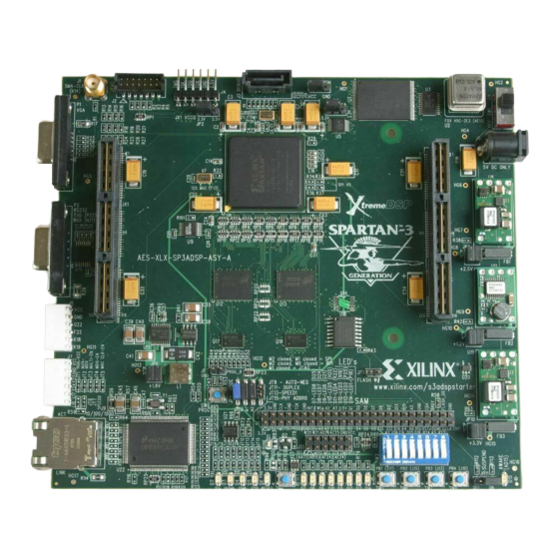
Design Description The Spartan-3A Starter Platform provides a platform for engineers designing with the Xilinx Spartan-3A DSP FPGA. The board provides the hardware to not only evaluate the advanced features of the Spartan-3A DSP, but also to implement complete user applications using peripherals on the Spartan-3A DSP Starter Platform and EXP modules, or both, plugged into EXP expansion connectors on the Spartan-3A DSP Starter Platform. -
Page 6: Ordering Information
Table 1 lists the evaluation kit part numbers. Table 1: Evaluation Kit and Hardware Ordering Information Part Number Hardware HW-SD1800A-DSP-SB-UNI-G XtremeDSP Starter Platform - Spartan-3A DSP 1800A Edition www.BDTIC.com/XILINX www.xilinx.com Spartan-3A DSP Starter Platform User Guide UG454 (v1.1) January 30, 2009... -
Page 7: Functional Description
Functional Description Functional Description A high-level block diagram of the Spartan-3A DSP Starter Platform is shown in Figure Subsequent sections provide details of the board design. X-Ref Target - Figure 1 3SD1800A-FG676 Configuration and Debug Memory System ACE 128 MB DDR2... -
Page 8: Xilinx Spartan-3A Dsp Fpga
Functional Description Xilinx Spartan-3A DSP FPGA The Xilinx XC3SD1800A-4FG676C device designed into the Spartan-3A DSP Starter Platform provides four I/O banks — two are fixed voltage and two are I/O voltage- selectable. The four I/O banks are described in Table 2 and detailed I/O pin usage is provided throughout this document. -
Page 9: Memory
DDR2) and non-volatile ROM (16Mbytes parallel, and 64Mbit serial) to support various types of applications. Additionally, a 50-pin connector is provided for SystemACE interface (not included) that can be used to configure the Spartan-3A DSP FPGA, and to provide storage for A/V media files from removable Compact Flash cards. - Page 10 UG454_03_050908 Figure 3: DDR2 SDRAM Interface The following guidelines were used in the design of the DDR2 interface to the Spartan-3A DSP FPGA. These guidelines are based on Micron recommendations and board level simulation. Ideal impedance values are listed. Actual values may vary.
- Page 11 FPGA_DDR_D1 FPGA_DDR_A7 FPGA_DDR_D2 FPGA_DDR_A8 FPGA_DDR_D3 FPGA_DDR_A9 FPGA_DDR_D4 FPGA_DDR_A10 FPGA_DDR_D5 FPGA_DDR_A11 FPGA_DDR_D6 FPGA_DDR_A12 FPGA_DDR_D7 FPGA_DDR_BS0 FPGA_DDR_D8 FPGA_DDR_BS1 FPGA_DDR_D9 FPGA_DDR_RAS# FPGA_DDR_D10 FPGA_DDR_CAS# FPGA_DDR_D11 FPGA_DDR_WE# FPGA_DDR_D12 FPGA_DDR_CS# FPGA_DDR_D13 FPGA_DDR_CKE FPGA_DDR_D14 www.BDTIC.com/XILINX Spartan-3A DSP Starter Platform User Guide www.xilinx.com UG454 (v1.1) January 30, 2009...
-
Page 12: Intel J3 Parallel Flash
Jumper JP1 may be used to write-protect the Flash memory by placing a shunt across pins 2 and 3. Default setting is JP1 1:2. Table 4 details the Parallel Flash FPGA interface pinout. www.BDTIC.com/XILINX www.xilinx.com Spartan-3A DSP Starter Platform User Guide UG454 (v1.1) January 30, 2009... -
Page 13: Intel S33 Serial Flash
J3 Flash Signal FPGA Pin J3 Flash Signal FPGA Pin SPISEL_1 * SPI_SEL# SPISEL_1 * SPI_CLK AE24 SPISEL_1 AD26 * SPI_MOSI AB15 SPISEL_1 AC25 * SPI_MISO AF24 www.BDTIC.com/XILINX Spartan-3A DSP Starter Platform User Guide www.xilinx.com UG454 (v1.1) January 30, 2009... -
Page 14: Systemace Module (Sam) Connector
SystemACE Module (SAM) Connector The Spartan-3A DSP Starter Platform provides a SAM 50-pin connector (J8) for SystemACE interface that can be used to configure the Spartan-3A DSP FPGA, and provide storage for A/V media files from removable Compact Flash cards. The Avnet SystemACE Module (DS-KIT-SYSTEMACE) can be used to perform both of these functions. -
Page 15: Interfaces
The Spartan-3A DSP FPGA has access to Ethernet and RS232 physical layer transceivers for communication purposes. Network access is provided by a 10/100/1000 Mb/s Ethernet PHY, which is connected to the Spartan-3A via a standard GMII interface. The PHY connects to the outside world with a standard RJ45 connector. Serial port communication to the FPGA fabric is provided through an RS232 transceiver using a DB9 DCE female connector. -
Page 16: National Semiconductor 10/100/1000 Ethernet Phy
MDIA_N Spartan MDIA_P 3A DSP MDIA_N FPGA MDIA_P data_rx[7:0] MDIA_N clk_rx control_rx Crystal 25 MHz gbe_mclk clk_to_MAC gbe_rstn reset# LEDs UG454_05_050908 Figure 5: 10/100/1000 Mb/s Ethernet Interface www.BDTIC.com/XILINX www.xilinx.com Spartan-3A DSP Starter Platform User Guide UG454 (v1.1) January 30, 2009... - Page 17 Single node (NIC) and CLK_TO_MAC enabled. These and other settings are enabled by three-pad jumpers with a resistor connecting either pads 1 and 2 or pads 2 and 3. www.BDTIC.com/XILINX Spartan-3A DSP Starter Platform User Guide www.xilinx.com UG454 (v1.1) January 30, 2009...
- Page 18 Multiple Node Enable JT3: Pins 2-3 Multiple node priority – switch/hub JT5: Pins 1-2 CLK_TO_MAC output enabled (default) Clock to MAC Enable JT5: Pins 2-3 CLK_TO_MAC output disabled www.BDTIC.com/XILINX www.xilinx.com Spartan-3A DSP Starter Platform User Guide UG454 (v1.1) January 30, 2009...
-
Page 19: Rs232
SPI port, or can be used as 4 general purpose I/Os. Figure 6 shows the pinout of the Digilent headers; Table 11 provides the FPGA pinout. www.BDTIC.com/XILINX Spartan-3A DSP Starter Platform User Guide www.xilinx.com UG454 (v1.1) January 30, 2009... - Page 20 Table 12 identifies the connection of the J3 signals to the FPGA. Table 12: Debug Connector (J3) J3 Pin Number Signal Name FPGA Pin — DBG_Tx_n DBG_Tx_p www.BDTIC.com/XILINX www.xilinx.com Spartan-3A DSP Starter Platform User Guide UG454 (v1.1) January 30, 2009...
-
Page 21: Vga Output
DBG_Rx_n DBG_Rx_p — VGA Output The Spartan-3A DSP Starter Platform includes a VGA video output using a resistor-divider network and 4-bits per RGB color as shown in Figure 7. This resistor-divider network is 510, 1K, 2K, & 4K ohms for each color. The outputs of the three resistor-divider networks are presented to DB15 connector P1. -
Page 22: Miscellaneous I/O
Miscellaneous I/O An 8-position DIP switch, 4 user Pushbuttons, and 8 user LEDs are provided on the Spartan-3A DSP Starter Platform. The connection of these devices to the FPGA is detailed Table 14. The DIP switch is connected to FPGA Bank 0 and each switch is pulled low in the “OFF”... -
Page 23: Expansion Connectors
EXP modules or a single dual slot EXP module. Both off-the-shelf EXP modules and user-developed modules can easily be plugged onto the Spartan-3A DSP Starter Platform to add features and functions to the backend application of the main board. - Page 24 Differential clock output pairs Total The Spartan-3A DSP FPGA user I/O pins that connect to the two EXP connectors are shown in the following tables. The Samtec QTE connector plugs on the Spartan-3A DSP Starter Platform (part number: QTE-060-09-F-D-A) mate with the Samtec QSE high- performance receptacles (part number: QSE-060-01-F-D-A), located on the daughter card.
- Page 25 EXP1_DIFF_p21 EXP1_DIFF_n20 EXP1_DIFF_n21 EXP1_DIFF_p18 EXP1_SE_IO_32 EXP1_DIFF_n18 EXP1_SE_IO_33 EXP1_DIFF_p16 EXP1_DIFF_p19 EXP1_DIFF_n16 EXP1_DIFF_n19 EXP1_DIFF_CLK_OUT_p EXP1_DIFF_p17 EXP1_DIFF_CLK_OUT_n EXP1_DIFF_n17 EXP1_DIFF_p14 EXP1_DIFF_p15 EXP1_DIFF_n14 EXP1_DIFF_n15 EXP1_DIFF_p12 EXP1_DIFF_p13 EXP1_DIFF_n12 EXP1_DIFF_n13 3.3V 3.3V 3.3V 3.3V www.BDTIC.com/XILINX Spartan-3A DSP Starter Platform User Guide www.xilinx.com UG454 (v1.1) January 30, 2009...
- Page 26 EXP2_SE_IO_5 AE23 AC20 EXP2_SE_IO_6 EXP2_SE_IO_7 AF23 2.5V 2.5V AA17 EXP2_SE_IO_8 EXP2_SE_IO_9 AD22 AC19 EXP2_SE_IO_10 EXP2_SE_IO_11 AE21 2.5V 2.5V AB18 EXP2_SE_IO_12 EXP2_SE_IO_13 AD21 EXP2_SE_IO_14 EXP2_SE_IO_15 AC21 2.5V 2.5V www.BDTIC.com/XILINX www.xilinx.com Spartan-3A DSP Starter Platform User Guide UG454 (v1.1) January 30, 2009...
- Page 27 AA12 EXP2_DIFF_n16 EXP2_DIFF_n19 AC12 EXP2_DIFF_CLK_OUT_p EXP2_DIFF_p17 AE17 EXP2_DIFF_CLK_OUT_n EXP2_DIFF_n17 AD17 EXP2_DIFF_p14 EXP2_DIFF_p15 AF20 EXP2_DIFF_n14 EXP2_DIFF_n15 AE20 AD11 EXP2_DIFF_p12 EXP2_DIFF_p13 AC11 EXP2_DIFF_n12 EXP2_DIFF_n13 3.3V 3.3V AF14 EXP2_RCLK_DIFF_p10 EXP2_DIFF_p11 www.BDTIC.com/XILINX Spartan-3A DSP Starter Platform User Guide www.xilinx.com UG454 (v1.1) January 30, 2009...
-
Page 28: Configuration
14-pin 2mm spaced header (J2) with a ribbon cable or to the 0.1” header (J4) with flying leads. If the Xilinx Parallel Cable IV is used, the ribbon cable connector mates with the keyed J2 connector. The Xilinx Platform USB cable will also mate directly with J2. -
Page 29: Configuration Modes
X-Ref Target - Figure 9 UG454_09_050908 Figure 9: Configuration Connectors Configuration Modes The following table shows the Spartan-3A DSP configuration modes set by Jumper JP9. All mode jumpers (including the PUDC_B pin) are pulled up; jumper installation grounds the connection. Figure 10 depicts configuration jumper JP9;... -
Page 30: Board Power
+2.5V and +3.3V power rails. The +1.2V power rail (VCC_INT) is produced by a Texas Instruments PTH04000WAZ 3A power module. These switching converters can exhibit switching spikes in the 650 kHz – 750 kHz region; www.BDTIC.com/XILINX www.xilinx.com Spartan-3A DSP Starter Platform User Guide UG454 (v1.1) January 30, 2009... - Page 31 The user may experiment with the Spartan-3A DSP low-power SUSPEND mode by jumpering JP11 pins 2:3 (default 1:2). The AWAKE LED (D15) indicates the SUSPEND mode status.
-
Page 32: Board Clocks
Number of 11 15 11 11 11 25 10 Capacitors Board Clocks There are four clock sources provided on the Spartan-3A DSP Starter Platform: • A 125 MHz oscillator connected to GCLK7 (Bank 0). • A 25.175 MHz oscillator (primarily for VGA timing) connected to RHCLK2 (Bank 1). -
Page 33: Pcb Stackup
UG454_012_050908 Figure 12: PCB Stackup Related Resources Xilinx would like to acknowledge the following key partners for their key contributions to this project. For more information about this product, reference designs, and additional documentation, please visit the product home page found at www.xilinx.com/s3adspstarter... - Page 34 Texas Instruments www.ti.com www.ti.com/power www.ti.com/xilinx Regulators focus.ti.com/docs/prod/folders/print/pth04000w.html focus.ti.com/docs/prod/folders/print/pth05050w.html focus.ti.com/docs/prod/folders/print/tps51116.html Supervisors focus.ti.com/docs/prod/folders/print/tps3828-50.html focus.ti.com/docs/prod/folders/print/tps3808g01.html focus.ti.com/docs/prod/folders/print/tps3307-25.html RS232 focus.ti.com/docs/prod/folders/print/max3221e.html Intel www.intel.com www.intel.com/design/flcomp/prodbref/s33.htm?iid=ipp_embed+flash_s33& www.intel.com/design/flcomp/prodbref/308275.htm?iid=ipp_embed+flash_j3d& www.foxonline.com/ www.foxonline.com/xpresso_xo.htm www.foxonline.com/smd_xtals.htm www.foxonline.com/thruhole_osc.htm National Semiconductor www.national.com www.national.com/pf/DP/DP83865.html www.BDTIC.com/XILINX www.xilinx.com Spartan-3A DSP Starter Platform User Guide UG454 (v1.1) January 30, 2009...
- Page 35 Related Resources Samtec www.samtec.com/ www.samtec.com/technical_specifications/overview.aspx?series=QTE Tyco/Amp www.tycoelectronics.com/ http://catalog.tycoelectronics.com/TE/bin/TE.Connect?C=1&M=BYPN&PID=407634& PN=1-6605833-1&I=13 www.BDTIC.com/XILINX Spartan-3A DSP Starter Platform User Guide www.xilinx.com UG454 (v1.1) January 30, 2009...
- Page 36 Related Resources www.BDTIC.com/XILINX www.xilinx.com Spartan-3A DSP Starter Platform User Guide UG454 (v1.1) January 30, 2009...
- Page 37 X-Ref Target - Figure A-1 JP10 JP11 JT1 through JT7, JT8 through JT15, inclusive inclusive UG454_A01_050908 Figure A-1: Connector, Header, and Jumper Locations www.BDTIC.com/XILINX Spartan-3A DSP Starter Platform www.xilinx.com UG454 (v1.1) January 30, 2009...
- Page 38 Spartan-3A DSP Starter Platform UG454 (v1.1) January 30, 2009...
Need help?
Do you have a question about the Spartan-3A and is the answer not in the manual?
Questions and answers