
Related Manuals for TTI TSX Series


Summary of Contents for TTI TSX Series
- Page 1 TSX Series High Current Power Supplies Service Manual Book Part Number 48511-0240 - Issue 2...
-
Page 2: Table Of Contents
Table of Contents General Specification Main Board Circuit Description Overview Mains Input, Switchmode and Linear Power Sections Linear Regulator Control and supervisory Sections Control Board Circuit Description (non-programmable versions only) CPU Board Circuit Description (Programmable versions only) Test & Calibration Procedure Important Electrical Safety Considerations Temporary Earthing for Primary Side Measurements Order of Checks and Adjustments... -
Page 3: General
General This manual has been prepared to aid the experienced engineer in the maintenance and repair of this series of high current power supplies. For detailed operating information the user should refer to the appropriate instruction manual. Service Precautions Recalibration or repair should only be attempted by skilled personnel in conjunction with high quality test equipment. -
Page 4: Specification
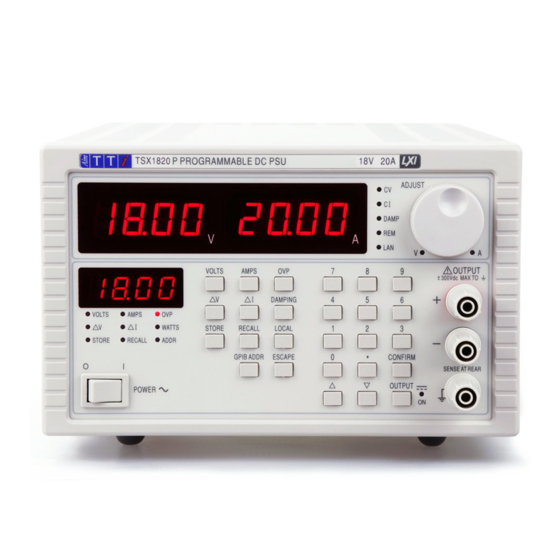
Specification Output Specifications Operating modes: Constant voltage or constant current with automatic crossover. Voltage Range: 0V to 35.3V (35V/10A), 0V to 18.15V (18V/20A) Current Range: 0.01A to 10.2A (35V/10A), 0.01A to 20.2A (18V/20A) Overvoltage protection range: 1V to 40V (35V/10A), 1V to 25V (18V/20A) Setting Resolution: 10mV, 10mA Load Regulation:... - Page 5 Note: All voltage and current levels set via the keyboard are displayed on a separate 0.0.3" 4- digit display. This entry preview system ensures that the user can observe the value entered before it is effected thus avoiding possible error. The display is also used for setting additional functions.
-
Page 7: Main Board Circuit Description
Main Board Circuit Description Overview The main board comprises a mains driven HF switchmode DC-DC isolating convertor using pulse width modulation (PWM) which feeds a linear regulator operating at low input-output voltage difference as shown in the skeleton circuit diagram opposite. Mains Input, Switchmode and Linear Power Sections Component references are to sheet 1 of the circuit diagram unless stated. - Page 8 HF Switch Drive - IC1 PWM outputs A and B are applied via driver IC11 to each end of drive transformer T3 primary, providing alternating antiphase PWM outputs of about 12V peak from each secondary. Gate resistors R18,R22 slow Q1,Q2 switching transitions to about 100nsec to limit RFI generation.
- Page 9 Auxiliary Supplies - Several control auxiliary supplies are derived from 50/60 Hz auxiliary transformer T1 secondaries: +5V 270mA DC via BR2,C27,IC4 for linear control, ADC, (DACs) and drive for the two meter LED displays. (ii) –5V 50mA DC via D2,C28,IC3 for linear control, ADC (and DACs). (iii) 3V 1.5A DC floating, unstabilised via D18,D42,D26 for driver Q4 collector.
-
Page 10: Linear Regulator Control And Supervisory Sections
Linear Regulator Control and supervisory Sections Component references are to sheet 2 of the circuit diagram unless stated. Note that 0V and the returns for the +5V and -5V auxiliary supplies for this circuitry are effectively at the positive output terminal potential of the power supply. Voltage Control Amplifiers - When the output is switched on CMOS analogue selector IC7-A applies the voltage programme voltage at PJ1-19 to the input of noninverting buffer amplifier IC5- C and amplifier input current is removed via R74,IC7-C in non-programmable versions. - Page 11 System Shutdown - Shutdown of both switchmode and linear regulators is asserted via IC9-A of the supervisory logic following power up, detection of inadequate auxiliary supplies, tripping of the master fault latch or, in programmable versions, during CPU board driven resetting of that latch. Output Circuit Components - C16 and C34 assist linear regulator stability.
-
Page 12: Control Board Circuit Description (Non-Programmable Versions Only)
Control Board Circuit Description (non-programmable versions only) The control pcb contains the voltage and current measurement system, the display, the controls for adjustment of the output voltage, current limit and over voltage protection, plus the output on/off switch connection. The pcb is connected to the main pcb by a 34-way flat cable. The control board also contains three preset adjustments. - Page 13 The over voltage protection user preset potentiometer VR3 is fed from the same +2.45V reference voltage as the other controls but connected from the main PCB via PJ1-15 as OVPREF+. The OVP set from VR3 wiper OVPSET is fed to the OVP trip comparator IC6-A on the main board via PJ1-18;...
-
Page 14: Cpu Board Circuit Description (Programmable Versions Only)
CPU Board Circuit Description (Programmable versions only) Overview The power supplies use a Z80 microprocessor to accept and process commands (from the keyboard, RS232 interface or GPIB interface) and to pass on the necessary command and control information to a microcontroller, located on the other side of an opto-isolated interface, which controls the setting of the values for voltage, current and OVP and the measurement of output voltage and current. - Page 15 Microcontroller Circuit This section contains the voltage and current measurement system, the display drivers and the DACs which are used to set the output voltage, current limit and over voltage protection. The measurement system and display is controlled by a microcontroller IC26. The two 4-digit LED displays on the front panel board are driven by IC26 via the segment latch IC30 and the digit latch IC31.
-
Page 16: Test & Calibration Procedure
Test & Calibration Procedure Important Electrical Safety Considerations A substantial proportion of the power supply main PCB is occupied by primary side circuitry comprising tracks, terminals and components (including one of the large heat sinks) which normally operate at AC mains potential. The incoming AC supply to the PCB or PSU under test must be isolated by means of a 1:1 isolation transformer of at least 700VA rating for safety and noise control. -
Page 17: Test Equipment For Main Pcb Testing
Test Equipment for Main Pcb Testing 100Ω 5W wirewound resistance for discharging HV reservoirs. Power supplies: 60VDC 2A limited, 5VDC 2A limited, 3VDC 1.5A limited. A single 60V 2A dual lab supply should meet all requirements. A 4700uF 63V electrolytic capacitor is required across the 60V output while checking overcurrent tripping. -
Page 18: Linear Regulator Checks
Linear Regulator Checks Check/Preadjust Voltage Zero - Connect an external +5VDC, 2A limited power supply between DCVOUT (+ve) and VOUT- (access top R55 and D37 respectively). Set Voltage control(s) to minimum and Current control to maximum. Switch Output on. Switch supplies on. -
Page 19: Testing Of Main Pcbs At Full Voltage
Check/Set Pre-regulator Gain - Connect CRO between 0V and OPTPO1B. Reduce Voltage controls for 5.0/3.2V *? DC output. The voltage across R128 (generated by the optocoupler input current) should be 175 to 200mV; otherwise switch off, discharge HV reservoirs C9,10 and fit E12 0.25W resistor in R128 to bring the voltage into range on retest. -
Page 20: Recalibration Of Assembled Power Supplies
board) for about 34V OVP display. Rotate VR10 fully ACW. The display should indicate "TRIP". Switch off. Allow time or discharge HV reservoirs C9,10. Recalibration of Assembled Power Supplies Preparation - Ensure voltage selector is in the appropriate position and HV bridging connector present. -
Page 21: Parts List
Parts List PCB ASSY MAIN (10A) - (44115-0350) - COMMON PARTS PCB ASSY MAIN (20A) - (44115-0300) - COMMON PARTS Part Number Description Position 20030-0240 WASHER 4BA ZPST FOR SK1,2 20030-0263 WASHER M3 ZPST FOR T1,TC1,Q1,2,TS1,2,IC4,PCB 20038-9501 WASHER M3 Spring FOR T1,TC1,Q1,2,TS1,2,IC4,PCB 20038-9503 WASHER M3.5 SPRING... - Page 22 PCB ASSY MAIN (10A) - (44115-0350) - COMMON PARTS/continued... PCB ASSY MAIN (20A) - (44115-0300) - COMMON PARTS/continued... Part Number Description Position 22573-0202 HEADER 2 WAY STRAIGHT .156P PJ2,3 22573-0204 HEADER 4 WAY STRAIGHT .156P 22575-0100 HEADER 34 WAY (2X17) STR SKELN 23183-1220 RES 220RJ 1W CF 23183-4100...
- Page 23 PCB ASSY MAIN (10A) - (44115-0350) - COMMON PARTS/continued... PCB ASSY MAIN (20A) - (44115-0300) - COMMON PARTS/continued... Part Number Description Position 23185-4270 RES 270KJ W25 CF RD25S B/R R127 23185-4330 RES 330KJ W25 CF RD25S B/R R132 23185-5100 RES 1M0J W25 CF RD25S B/R R140 23185-5220 RES 2M2J W25 CF RD25S B/R...
- Page 24 PCB ASSY MAIN (10A) - (44115-0350) - COMMON PARTS/continued... PCB ASSY MAIN (20A) - (44115-0300) - COMMON PARTS/continued... Part Number Description Position 23427-0331 CAP 1N0K 63V CER RD870-6B102 C14,15,29 23427-0334 CAP 470PK 100V MED K P5 23427-0353 CAP 220PG 100V CER N750 P5T C37,40,62 23438-0007 CAP 100NS 63V CER P5...
- Page 25 PCB ASSY MAIN (10A) - (44115-0350) - COMMON PARTS/continued... PCB ASSY MAIN (20A) - (44115-0300) - COMMON PARTS/continued... Part Number Description Position 25130-0903 DIO ZEN 5V1 W4 25130-0906 DIO ZEN 4V3 W4 25210-030 TRIAC TAG T0805MH 25211-0301 RECTIFIER BRIDGE D20XB60 25211-9302 RECTIFIER BRIDGE W02G BR1,2...
- Page 26 PCB ASSY MAIN (10A) - (44115-0350) - UNIQUE PARTS Part Number Description Position 20030-0263 WASHER M3 ZPST FOR Q14,15 20038-9501 WASHER M3 Spring FOR Q14,15 20210-0101 NUT M3 ZPST FOR Q14,15,TS2 20234-0024 SCREW M3 X 16 PNHDPZ ZPST FOR Q15 20611-0003 BUSH POLYESTER TO220 J22-5006 FOR Q14,15...
- Page 27 PCB ASSY MAIN (20A) - (44115-0300) - UNIQUE PARTS/continued... Part Number Description Position 20062-9303 SCREW NO 6 X 0.5" PNHDPZ ST/AB FOR SK3 (2) 20062-9304 SCREW No.6x5/8" Pozi. Pan FOR SK3 20210-0101 NUT M3 ZPST FOR Q9,10,11,12,TS3 20234-0024 SCREW M3 X 16 PNHDPZ ZPST FOR Q9,11 20611-0003 BUSH POLYESTER TO220 J22-5006...
- Page 28 PCB ASSY CPU - (44115-0330) Part Number Description Position 10366-9701 ADHESIVE Mtg Pads 25 x 12mm FOR BATTERY 20030-0263 WASHER M3 ZPST FOR IC36 20038-9501 WASHER M3 Spring FOR IC36 20210-0101 NUT M3 ZPST IC36,PJ2 20234-0011 SCREW M3 X 10 PNHDPZ NPST IC36,PJ1,PJ2 20611-0003 BUSH POLYESTER TO220 J22-5006...
- Page 29 PCB ASSY CPU - (44115-0330)/continued... Part Number Description Position 23557-0634 CAP 4U7 63V ELEC P2 23557-0647 CAP 10U 35V ELEC RE2 P2 C3,10,11,13,14,24 23557-0657 CAP 100U 10V ELEC RE2 P2 C5,6,9,61 23557-0660 CAP 2200U 16V ELEC RE2 P5 23557-0673 CAP 22U 35V ELEC RE2 P2 23620-0246 CAP 100NK 63V P/E P5 C16,18,25,26,28-48,50-60...
- Page 30 PCB ASSY CPU - (44115-0330)/continued... Part Number Description Position 27234-5730 IC 74AC573 IC17,30,37,39 27250-0050 IC 14C88 IC16 27250-0060 IC 14C89 IC25 27250-0200 IC Z80B CMOS CPU 27250-0410 IC UPD7210C GPIB CONT 27250-0450 IC UPD71051C 27250-2000 IC MCU8 PIC16C55XT-P IC26 27400-0080 IC 27C256 32Kx8 EPRM 200ns IC10 27410-0420...
- Page 31 PCB ASSY CONTROL (10A) (44115-0310) - COMMON PARTS/continued... PCB ASSY CONTROL (20A) (44115-0320) - COMMON PARTS/continued... Part Number Description Position 23557-0611 CAP 47U 10V ELEC RE2 P2 C7,8 23557-0657 CAP 100U 10V ELEC RE2 P2 23620-0246 CAP 100NK 63V P/E P5 C2,4,6,14-21 23620-0249 CAP 330NK 63V P/E P5...
- Page 32 PCB ASSY KEYBOARD - (44115-0340) Part Number Description Position 10148-0005 CABLE 26W IDC FLAT GREY AWG-28 22226-0140 KEYSWITCH DARK GREY K0-26 22573-0056 HEADER 16 WAY STR SIL (6.8MM) FOR DISPLAYS 22575-0046 CONN TRANSITION 26W IDC 22575-0050 CONN TRANSITION 20W IDC 22575-0051 SKT 20W IDC HIF3BA-20D-2.54R 22575-0102...
- Page 33 REAR PANEL ASSY - (46912-0400)/continued... Part Number Description Position 20038-9502 WASHER M4 SPRING TERMINAL BARRIER, EARTHING TAG 20210-0101 NUT M3 ZPST IEC INLET, BLANKING PIECES 20210-0102 NUT M4 ZPST TERMINAL BARRIER, EARTHING TAG 20213-0010 CAPTIVE NUT SNU-1219-17-00 20234-0025 SCREW M3 x 12 PNHDPZ ZPST IEC INLET 20234-0027 SCREW M3 x 6 PNHDPZ ZPST...
- Page 34 FRONT PANEL ASSY - (10A) (46912-0410)/continued... FRONT PANEL ASSY - (20A) (46912-0420)/continued... Part Number Description Position 33331-1920 OVERLAY FRONT PANEL - 10A 33331-1970 OVERLAY FRONT PANEL - 20A FRONT PANEL ASSY - (10A) PROG (46912-0430) FRONT PANEL ASSY - (20A) PROG (46912-0440) Part Number Description Position 20030-0263...
- Page 35 35V/10A - CASE PARTS (51153-0601) ) 18V/20A - CASE PARTS (51153-0701) ) - COMMON 35V/10A PROG - CASE PARTS (51153-0651) ) 18V/20A PROG - CASE PARTS (51153-0751) ) Part Number Description Position 20030-0266 WASHER M4 ZPST FEET, CPU PILLARS 20030-0267 WASHER M5 ZPST RUBBER FEET 20037-0247...
- Page 36 35V/10A - CASE PARTS - UNIQUE 18V/20A - CASE PARTS - UNIQUE Part Number Description Position 20030-0263 WASHER M3 ZPST BLANKING PIECES 20234-0012 SCREW M3 X 8 PNHDPZ ZPST BLANKING PIECES 20657-0072 CAP BLK LINE C211 GREY 99 20657-0070 KNOB 21MM DA217 180 GREY 99 31334-0100 BLANKING PIECE - 9WAY "D"...
-
Page 37: Manufacturing Changes
Manufacturing Changes From March 1993 additional 4N7 'Y' rated (250V) capacitors (Part no. 23424- 0459) were added to the main board in positions C76 and C77, see Main Board circuit diagram sheet 1. These improve the rejection of large line-borne transients which in extreme circumstances could otherwise damage any or all of TC1, BR3, Q1, and Q2. - Page 38 From May 94 OPTO1 became an HCPL-4503 (Part No. 27001-0030), R133 became 3k3 and R128 a S.O.T. (typically 68Ω); the main pcb became Iss 5 to accommodate this 8-pin device. The high C.M.M.R. of this opto improved immunity to conducted interference from both AC input and DC output terminals.
-
Page 39: Circuit Diagrams
Circuit Diagrams... - Page 49 Thurlby Thandar Instruments Ltd Glebe Road, Huntingdon, Cambridgeshire PE29 7DR, England Telephone: (44) 01480 412451 Fax: (44) 01480 450409 e mail: sales@tti-test.com web site: www.tti-test.com...
Need help?
Do you have a question about the TSX Series and is the answer not in the manual?
Questions and answers