
Related Manuals for Tektronix P6467


Summary of Contents for Tektronix P6467
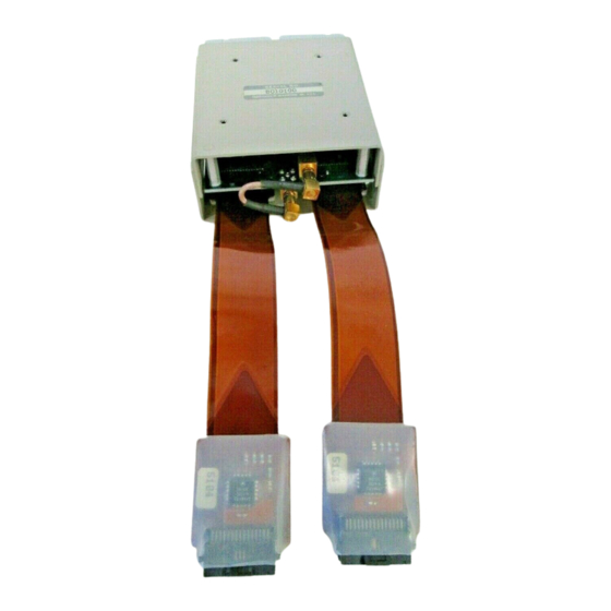
- Page 1 sales@artisantg.com artisantg.com (217) 352-9330 | Visit our website - Click HERE...
- Page 2 Instruction Manual P6467 High-Speed Probe Adapter 070-9176-00 Warning The servicing instructions are for use by qualified personnel only. To avoid personal injury, do not perform any servicing unless you are qualified to do so. Refer to the Safety Summary prior to...
- Page 3 Commercial Computer Software – Restricted Rights clause at FAR 52.227-19, as applicable. Tektronix products are covered by U.S. and foreign patents, issued and pending. Information in this publication supercedes that in all previously published material. Specifications and price change privileges reserved.
- Page 4 Tektronix warrants that the products that it manufactures and sells will be free from defects in materials and workmanship for a period of one (1) year from the date of shipment. If a product proves defective during this warranty period, Tektronix, at its option, either will repair the defective product without charge for parts and labor, or will provide a replacement in exchange for the defective product.
- Page 6 ..........P6467 High-Speed Probe Adapter Instruction Manual...
-
Page 7: Table Of Contents
........Appendicies Appendix A: P6467 High-Speed Probe Adapter Input Connector . . . - Page 8 ..........Figure 4: Clock Jumper Locations on the P6467 Probe .
- Page 9 Table 9: HFS 9003 Stimulus System Menu Setups ....Table 10: HFS 9003 Stimulus System to P6467 Test Board Connections Table 11: Jumper Positions for the Setup & Hold and Maximum Operating Frequency Check .
- Page 10 If you suspect there is damage to this product, have it inspected by qualified Suspected Failures service personnel. Do Not Immerse in Liquids Clean the probe using only a damp cloth. Refer to cleaning instructions. P6467 High-Speed Probe Adapter Instruction Manual...
- Page 11 Overvoltage categories are defined as follows: CAT III: Distribution level mains, fixed installation CAT II: Local level mains, appliances, portable equipment CAT I: Signal level, special equipment or parts of equipment, telecommunica- tion, electronics P6467 High-Speed Probe Adapter Instruction Manual...
- Page 12 Dangerous voltages or currents may exist in this product. Disconnect power, With Power On remove battery (if applicable), and disconnect test leads before removing protective panels, soldering, or replacing components. To avoid electric shock, do not touch exposed connections. P6467 High-Speed Probe Adapter Instruction Manual...
- Page 13 Service Safety Summary viii P6467 High-Speed Probe Adapter Instruction Manual...
- Page 14 Preface The P6467 Instruction Manual is intended to help you setup and use the P6467 High-Speed Probe Adapter to acquire data from a system-under-test through a DAS/NT, DAS/XP, or a TLA 520 logic analyzer. The manual contains the following sections:...
- Page 15 DAS/XP digital analysis systems to acquire data with the 92A96 Data Acquisition Modules. TLA 510 & TLA 520 User Manual. This manual describes how to use the Tektronix Logic Analyzers to acquire and display data with the 92A96 Data Acquisition Modules. DAS 9200 Programmatic Command Language User Manual. This manual describes how to use the Programmatic Command Language through GPIB or 92LAN to control the DAS from a remote location.
- Page 16 Getting Started This chapter provides an overview of the P6467 High-Speed Probe Adapter. It also describes the accessories available with the P6467 Probe as well as installation and configuration instructions. Product Description The P6467 High-Speed Probe Adapter is designed for the DAS/NT, DAS/XP, or TLA 500 series logic analyzers with the 92A96 or 92C96 Data Acquisition Modules.
- Page 17 92A96 Modules. If you purchased a 92A96 Module with your P6467 probe, refer to the DAS System User Manual or to the 92A96 and 92C96 Module User Manual for instructions to install a 92A96 Module in a DAS mainframe.
-
Page 18: Figure 1: Probe Connections And Clock Jumpering For Two Single-Card Modules
Getting Started Configure and Install the Before you use the P6467 probe you must determine the operating mode and the Probes clocking requirements for your application. The clocking requirements depend on the number of cards in your 92C96 modules. You must specify one P6467 probe as the Master Clock probe and set the jumpers accordingly. -
Page 19: Figure 2: Probe Connections And Clock Jumpering For Two Two-Card Modules
ORG - 2 ORG - 2 J100 J100 GRN - 1 GRN - 1 J200 J200 GRN - 2 GRN - 2 J100 J100 Figure 2: Probe Connections and Clock Jumpering for Two Two-Card Modules P6467 High-Speed Probe Adapter Instruction Manual... -
Page 20: Figure 3: Probe Connections And Clock Jumpering For Two Three-Card Modules
GRN - 1 GRN - 1 J100 J100 GRN - 2 GRN - 2 J200 J200 GRN - 3 GRN - 3 J100 J100 Figure 3: Probe Connections and Clock Jumpering for Two Three-Card Modules P6467 High-Speed Probe Adapter Instruction Manual... -
Page 21: Figure 4: Clock Jumper Locations On The P6467 Probe
THLD EXT/MSTR CLK (J1) Figure 4: Clock Jumper Locations on the P6467 Probe After determining the jumper locations on the probe, replace the probe cover and continue with the following steps: 1. Refer to Figure 5 and connect the probe power cable to the probes (each 92A96 Module can power two P6467). -
Page 22: Figure 5: Connecting The Power Cable To The Probe
3. Connect the power cable to the power connector on one of the 92A96 Modules in the logic analyzer. Power Connector socket (J5) Bend the power cable and push in until it snaps in Figure 5: Connecting the Power Cable to the Probe P6467 High-Speed Probe Adapter Instruction Manual... -
Page 23: Figure 6: Disconnecting The Power Cable From The Probe
Slide out Figure 6: Disconnecting the Power Cable from the Probe 4. Connect the P6467 Probes to the 92A96 Probe Cables; if necessary, refer to Figures 1 through 3 on pages 3 through 5 respectively. 5. Connect the flexible leads of the probe to the system-under-test. Refer to Figure 7 to ensure that you properly connect the probe to the system-under- test (pin 1 of the probe to pin 1 of the probe connector). -
Page 24: Figure 7: Connecting The Probe To The System-Under-Test
Figure 7: Connecting the Probe to the System-Under-Test Install the Software Install the P6467 support software from the floppy disk using the Install Application selection from the Disk Services menu. Insert the floppy disk in the disk drive and follow the on-screen instructions to load the support software. - Page 25 Configure and Install the Probes beginning on page 3. Adjust the Probe You can adjust the threshold voltage of the clock inputs on the P6467 probe to Threshold Voltage meet the needs of your application. You only need to adjust the threshold voltage on the Master Clock probe.
-
Page 26: Figure 8: Sample Trigger Menu (First Module)
Figure 8 shows an example of one of the Trigger menus (the Trigger menu must be the same for both modules in the module pair with the exception of the definition of the signals used between the two modules). Figure 8: Sample Trigger Menu (First Module) P6467 High-Speed Probe Adapter Instruction Manual... -
Page 27: Figure 9: Sample Trigger Menu (Second Module)
You can use the following checks as an incoming inspection to determine if further testing or repair is necessary. The checks consist of connecting the probe to the P6467 Test Board and acquiring data through individual channels. -
Page 28: Table 2: Jumper Positions For Functional Checks
The procedures also assume that you will use the setups stored on the hard disk from the P6467 Support Software. 1. Remove the cover from the P6467 Probe and set jumpers to the positions indicated in Table 2. Table 2: Jumper Positions for Functional... - Page 29 3. Connect the Probe Power cable from the power connector of one of the 92A96 Modules on the logic analyzer to the power connector on the P6467 Probe (if necessary refer to Figure 5 on page 7 for information on connect- ing the Power cable).
-
Page 30: Table 3: Functional Check Data
The check verifies the functionality of the clock signal and the one data channel. You can verify the functionality of the remaining data channels by moving the pulse generator connection from J1 of the P6467 Test Board to one of the other channels and repeating the test. The acquired data in the State Display menu should track the data channel as you connect each data channel to the pulse generator output. - Page 31 0005 00 0000 00 0005 00 15. Disconnect the INPUT DATA A flex lead from the P6467 Test Board and connect the INPUT DATA B flex lead. 16. Disconnect the blue-labeled probe cable from the top connector of the P6467 Probe and connect them to the bottom connector (OUTPUT DATA B).
- Page 32 Descriptions and locations of jumpers Probe Operation There are two basic operating modes for the P6467 probe that you can set by jumpers J2 and J3, NORM and DIV2. The following sections describe the operating modes and the clock distribution.
- Page 33 Master Clock probe to a second P6467 probe as shown in Figure 3 on page 5. The second P6467 probe provides the clock for the last acquisition card in the module.
-
Page 34: Figure 10: Acquired Raw Data
In many cases the resultant data may be difficult to use and interpret. The P6467 Probe comes with support software to transfer the acquired data to a host computer and to save the data in a manner that is easier to analyze. You can work with the acquired data directly with host computer applications, or you can save the data in a reference memory for use with the logic analyzer. -
Page 35: Figure 11: Saved Data From Figure 10
Figure 11: Saved Data from Figure 10. Descriptions and Locations of Connectors The P6467 Probe acquires data from a system-under-test and sends the data to the logic analyzer. One probe can aquire data from two 92A96 probe cables from two acquisition modules (one module pair). Figure 12 shows the connectors on the probe (probe covers removed). -
Page 36: Figure 12: P6467 Probe Connectors
J8 (Master Clock Delay) J6 (EXT CLK IN) J400 (INPUT DATA B) J100 (OUTPUT DATA A) Side J5 (Probe Power) J200 (OUTPUT DATA B) J7 (Master Clock Delay) Bottom Figure 12: P6467 Probe Connectors P6467 High-Speed Probe Adapter Instruction Manual... - Page 37 Descriptions and Locations of Jumpers Figure 13 shows the locations of the jumpers on the P6467 probe. The jumper positions determine the operating mode and clocking of the probe. The probe defined as the Master Clock probe must have the jumpers in the correct positions to operate correctly;...
-
Page 38: Figure 13: P6467 Clock Jumpers And Clock Threshold Adjustment
A description of each clock jumper follows: J1 (MSTR CLK / EXT). This jumper connects either the Clock B Master clock or an external clock from another P6467 probe to the 92A96 probe cables connected to J200 (bottom two connectors) on the probe. - Page 39 Operating Basics P6467 High-Speed Probe Adapter Instruction Manual...
- Page 40 P6467 reference memory commands LA-OffLine application examples The P6467 support software consists of commands to transfer acquired data to a host and to create reference memories. This chapter does not include an exhaustive list of commands and information about using the acquired data with host computer applications.
-
Page 41: Table 4: 92A96 Fields
All fields Data fields Timestamps User specfic For information using field 15, refer to the Tektronix Application Note number 57W-7194-1. Contact your local Tektronix representative for information on obtaining application notes. Data records returned by the command are in the same format as the data records returned by the PCL ACQDATA? query. - Page 42 Use the optional –t switch with the CARDATA command if you do not want to adjust the timestamp values. If you use the –t switch, duplicate timestamp values can appear in the resultant output. The –t switch can be helpful while debugging code for the system-under-test. P6467 High-Speed Probe Adapter Instruction Manual...
- Page 43 However, you should avoid using the –t switch when you create a reference memory for more than one pair of 92A96 Modules. Doing so can cause inconsistent results when you display the data in the State menu. P6467 High-Speed Probe Adapter Instruction Manual...
- Page 44 Alpha to the host file test1. 2. Use the PCLSTRIP command to remove the PCL command header and file-transfer format information. 3. Convert the raw data file to a LA-OffLine file named acq.tst1. 4. Delete the raw data file. P6467 High-Speed Probe Adapter Instruction Manual...
- Page 45 Reference P6467 High-Speed Probe Adapter Instruction Manual...
-
Page 46: Table 5: Signal Acquisition System
Specifications This chapter contains the complete specifications for the P6467 High-Speed Acquisition Probe. Within each section the specifications are arranged in the following functional groups: Signal Acquisition System, Power Distribution System, Environmental, and Mechanical. All specifications are warranted unless they are designated typical. Warranted characteristics are checked by procedures in the Performance Verification chapter beginning on page 37 ;... -
Page 47: Table 6: Power Distribution System
+30 C to +40 C, 70% to 75% Relative Humidity Nonoperating +30 C to +60 C, 90% to 95% Relative Humidity Dynamics Mechanical Shock Class 7 Limits Operating and Nonoperating Half sine, 100 g, 11 ms duration, three axis, three drops each axis P6467 High-Speed Probe Adapter Instruction Manual... -
Page 48: Table 8: Mechanical
Packaged for Domestic 1.47 kg (3.25 lbs) Shipment Physical Dimensions Height 43 mm (1.7 in) Width 88 mm (3.45 in) Depth 274 mm (10.8 in), includes flex cables Cooling Method Convection Construction Material Aluminum Covers P6467 High-Speed Probe Adapter Instruction Manual... - Page 49 Specifications P6467 High-Speed Probe Adapter Instruction Manual...
- Page 50 WARNING The following servicing instructions are for use only by qualified personnel. To avoid injury, do not perform any servicing other than that stated in the operating instructions unless you are qualified to do so. Refer to all Safety Summaries before performing any service.
- Page 52 A TLA 520 Logic Analyzer, DAS/NT, or DAS/XP Logic Analyzer with two 92A96 or 92C96 Data Acquisition Modules One or more P6467 High-Speed Probe Adapters with a Probe Power cable One Tektronix HFS 9003 Stimulus System with one HFS 9DG1 Data...
- Page 53 If your logic analyzer has the 92A96 Modules in different slots, you must adjust these procedures accordingly. 1. Remove the cover from each P6467 Probe that you are testing and set the cover aside.
- Page 54 Performance Verification NOTE. The P6467 Application Support software includes a predefined setup that you can restore and use with the following setups. To use the predefined setups, select the Save/Restore menu and restore the setup file named P6467_PVD. Otherwise continue with the following steps to manually set up the logic analyzer.
-
Page 55: Figure 14: Trigger Menu Setup
In the Clock menu, select the falling edge of Clock_2 instead of the rising edge. b. In the Trigger menu, assert Signal BtoA instead of Signal AtoB, and change the last event to monitor Signal AtoB instead of Signal BtoA. P6467 High-Speed Probe Adapter Instruction Manual... -
Page 56: Table 9: Hfs 9003 Stimulus System Menu Setups
Output On, Output On Signal Type Pulse Pulse Pulse Pulse 4. If desired, save the test setups of HFS 9003 Stimulus System; refer to your HFS 9003 user documentation for information on saving setups. P6467 High-Speed Probe Adapter Instruction Manual... -
Page 57: Table 10: Hfs 9003 Stimulus System To P6467 Test Board Connections
Performance Verification 5. Connect the data generator outputs to the inputs of the P6467 Test Board in the following manner: a. Connect the clock signal C1 to J13 on the test board. b. Refer to Table 10 and connect the outputs of the two HFS DG2 generators to the connections at J1 through J8 on the test board. - Page 58 2 ns to the left of the center graticule. 5. Move the FET probe to one of the data signals of J100 on the P6467 Test Board (if necessary refer to Table 15 on page 64 for the identification of the data signals at J100).
-
Page 59: Table 11: Jumper Positions For The Setup & Hold And Maximum
J3 (CLK A/MSTR CLK) CLK A J4 (DIV2/NORM) NORM 3. Connect the INPUT DATA A flex cable of the probe to the P6467 Test Fixture. 4. On the logic analyzer, select the State Display menu and select F1: START to start the check. -
Page 60: Table 12: Test Setups For The Norm Operating Mode
OUTPUT DATA B 20 MHz 7.0 ns 7.3 ns INPUT DATA B OUTPUT DATA B 20 MHz 3.1 ns 2.8 ns 10. Move jumpers J2 and J4 on the P6467 Probe to the DIV2 positions. P6467 High-Speed Probe Adapter Instruction Manual... -
Page 61: Table 13: Test Setups For The Div2 Operating Mode
LEAD DELAY of the data channels to 5 ns and the clock channel LEAD DELAY to 2.8 ns (T = 2.2 ns). The Setup time is checked when you set the hold clock channel LEAD DELAY to 7.3 ns (T = 2.3 ns). setup P6467 High-Speed Probe Adapter Instruction Manual... -
Page 62: Table 14: Jumper Positions And Clock Cable Connections
HFS 9003 Stimulus System listed in Table 9 on page 41 except for the frequency–change the frequency to 100 MHz. 1. Refer to Table 14 and set the P6467 Probe jumpers for each one of the clock configuration setups to verify the proper clock operation. - Page 63 Table 14. Also, verify the correct setups for the HFS 9003 Stimulus System. If the tests still fail after verifying all of the setups, repair is necessary. Contact your local Tektronix representative for repair and replacement information. P6467 High-Speed Probe Adapter Instruction Manual...
- Page 64 Adjustment Procedures There are no sevice adjustment procedures required for this product. P6467 High-Speed Probe Adapter Instruction Manual...
- Page 65 Adjustment Procedures P6467 High-Speed Probe Adapter Instruction Manual...
- Page 66 Operating Basics chapter for information on the location of jumpers and probe connections. CAUTION. Components on the P6467 Probe can be damaged by static discharge. Service the probe only in a static-free environment. Observe standard handling precautions for static-sensitive devices while servicing the probe. Always wear a grounded wrist strap, or equivalent, while servicing the probe.
- Page 67 Removal and Replacement Instructions The P6467 Probe has a limited number of components that can be replaced. All replaceable parts are listed in the Replaceable Parts chapter beginning on page 55. You can access all of components on the probe after removing the top cover.
- Page 68 Verify that the probe power cable is connected and delivers power to the probe. Check the fuses on the P6467 Probe. Verify that you have the correct clock selected in the Clock menu for both acquisition modules.
- Page 69 (A_Clock) from the flex cable at J300 is sent to the probe cable connected to J100. For any other P6467 probes that do not acquire any clock signals, the data passes from the flex leads through the probe to the 92A96 probe cables.
-
Page 70: Replacable Parts
Replaceable Parts This section contains a list of the replaceable modules for the P6467 High–Speed Probe Adapter. Use this list to identify and order replacement parts. Parts Ordering Information Replacement parts are available through your local Tektronix field office or representative. -
Page 71: Using The Replaceable Parts List
Using the Replaceable Parts List This section contains a list of the mechanical and/or electrical components that are replaceable for the P6467 High–Speed Probe Adapter. Use this list to identify and order replacement parts. The following table describes each column in the parts list. - Page 72 45 SALEM ST PROVIDENCE RI 02907 75915 LITTELFUSE TRACOR INC 800 E NORTHWEST HWY DES PLAINES IL 60016–3049 SUB OF TRACOR INC 80009 TEKTRONIX INC 14150 SW KARL BRAUN DR BEAVERTON OR 97077–0001 PO BOX 500 P6467 High-Speed Probe Adapter Instruction Manual...
- Page 73 0.15 TAIL,0.043 DIA CTR COND,0.040 SQ TAIL (J7,J8) –14 174–3126–XX CABLE ASSY,:COAX,;RFD,75 OHM,2.7L,SMB,FEMALE, TK2469 174–3126–XX RTANG,EACH END –15 259–0144–XX FLEX CIRCUIT:INTERCONNECT TO PROBE 80009 2590144XX ADAPTERBOARD,CAROM –16 159–0159–XX FUSE,WIRE LEAD:1.5A,125V,5 SEC, 75915 25101.5 (F1,F2) P6467 High-Speed Probe Adapter Instruction Manual...
- Page 74 Replacable Parts Figure 1: Exploded view P6467 High-Speed Probe Adapter Instruction Manual...
- Page 75 JR,4 POS(2X2) X (2) 1X3,0.1 CTR,LATCHING –7 348–0187–XX FOOT,CABINET:BLACK POLYURETHANE, 0JR05 ORDER BY DESC (THIS IS A SUB–PART OF TEST FIXTURE ITEM 3 ABOVE) 070–9176–XX MANUAL,TECH:INSTRUCTION,P6467,DP TK2547 070–9176–XX 070–8364–XX MANUAL,TECH:REFERENCE,DAS9200 92LANP,DP TK2548 PER TEK P/N P6467 High-Speed Probe Adapter Instruction Manual...
- Page 76 Replacable Parts Figure 2: Exploded view P6467 High-Speed Probe Adapter Instruction Manual...
- Page 77 Replacable Parts P6467 High-Speed Probe Adapter Instruction Manual...
-
Page 78: Appendix A: P6467 High-Speed Probe Adapter Input Connector
(AMP part number 104550-4) or a through-hole version (AMP part number 104078-4). Table 15, on the page 64, shows the pinouts of the connector on each P6467 Probe. The definition of the data pins depend on the 92A96 Probe Cable connection. -
Page 79: Table 15: P6467 Probe Pinouts
Appendix A: P6467 High-Speed Probe Adapter Input Connector Table 15: P6467 Probe Pinouts 92A96/C96 92A96/C96 92A96/C96 92A96/C96 Orange Probe Green Probe Blue Probe Gray Probe Buffer Assembly Pins Clock Pins Clk0 Clk1 Clk2 Clk3 Data Pins C0-7 C1-7 C2-7 C3-7... -
Page 80: Appendix B: P6467 Test Board
Performance Verification chapter on page 37. The P6467 Test Board is designed to accept a clock signal and data signals from a test generator and route them to a 30-pin connector to one of the flex leads of the P6467 Probe. - Page 81 Appendix B: P6467 Test Board P6467 High-Speed Probe Adapter Instruction Manual...
-
Page 82: Index
Index CONVERT command, 29 P6467 High-Speed Probe Adapter Instruction Manual... - Page 83 Index P6467 High-Speed Probe Adapter Instruction Manual...
Need help?
Do you have a question about the P6467 and is the answer not in the manual?
Questions and answers