
Related Manuals for Epson S5U13517P00C100


Summary of Contents for Epson S5U13517P00C100
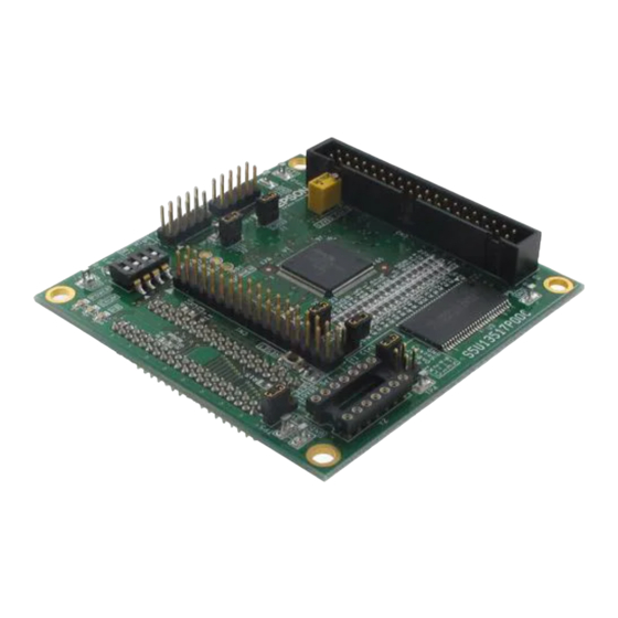
- Page 1 S1D13517 Display Controller S5U13517P00C100 Evaluation Board User Manual Document Number: X92A-G-001-01.1 Rev. 1.1...
- Page 2 This evaluation board/kit or development tool is intended for use by an electronics engineer and is not a consumer product. The user should use it properly and in a safe manner. Seiko Epson does not assume any responsibility or liability of any kind of damage and/or fire caused by the use of it.
-
Page 3: Table Of Contents
4.4.2 Connecting to the Epson S5U13U00P00C100 USB Adapter Board ..13 LCD Panel Interface ......14 GPO and PWM Connections . - Page 4 Seiko Epson Corporation S5U13517P00C100 Evaluation Board Rev. 1.1...
-
Page 5: Chapter 1 Introduction
S1D13517 Display Controller. The S5U13517P00C100 evaluation board can be used with many native platforms via the host connector which provides the appropriate signals to support a variety of CPUs. The S5U13517P00C100 evaluation board can also connect to the S5U13U00P00C100 USB Adapter board so that it can be used with a laptop or desktop computer, via USB 2.0. -
Page 6: Chapter 2 Features
Features Chapter 2 Features The S5U13517P00C100 Evaluation Board includes the following features: • S1D13517 Display Controller (128-pin QFP) • Integrated Silicon Solution, Inc. IS42S16800E-7TLI 128M-bit SDRAM (54-pin TSOP) • Header with all S1D13517 Host Bus Interface signals • Headers for connection to the S5U13U00P00C100 USB Adapter board •... -
Page 7: Chapter 3 Installation And Configuration
Installation and Configuration Chapter 3 Installation and Configuration The S5U13517P00C100 evaluation board incorporates a DIP switch, jumpers, and 0 ohm resistors which allow it to be used with a variety of different configurations. 3.1 Configuration DIP Switch The S1D13517 has 2 configuration inputs (CNF[1:0]). A DIP switch (SW1) is used to configure CNF[1:0] as described below. -
Page 8: Configuration Jumpers
Installation and Configuration 3.2 Configuration Jumpers The S5U13517P00C100 has 6 jumpers which configure various board settings. The jumper positions for each function are shown below. Jumper Function Position 1-2 Position 2-3 No Jumper COREVDD current COREVDD Normal — measurement IOVDD current... - Page 9 When the jumper is at position 3-4, the second oscillator is selected. When the jumper is at position 5-6, the CLKI pin is forced to GND. Figure 3-3: Configuration Jumper Location (J4, J5, J6) Seiko Epson Corporation S5U13517P00C100 Evaluation Board Rev. 1.1...
-
Page 10: Chapter 4 Technical Description
4.1 Power 4.1.1 Power Requirements The S5U13517P00C100 evaluation board requires an external regulated power supply (3.3V / 0.5A). The power is supplied to the evaluation board through pin 34 of the CN1 header, or pin 5 of the P2 header. -
Page 11: Clocks
The clock for the S1D13517 Display Controller is provided by a 24MHz oscillator. The S5U13517P00C100 evaluation board has a DIP14 footprint for an optional second oscillator, Y2. This is provided for cases requiring a different clock frequency for the S1D13517 Display Controller. To use Y2, an oscil- lator must be populated in the Y2 footprint and the J6 jumper placed at position 3-4. -
Page 12: Host Interface
4.4 Host Interface 4.4.1 Direct Host Bus Interface Support All S1D13517 host interface pins are available on connector CN1 which allows the S5U13517P00C100 evaluation board to be connected to a variety of development platforms. The following figure shows the location of host bus connector CN1. CN1 is a 0.1x0.1 inch 34-pin header (17x2). -
Page 13: Connecting To The Epson S5U13U00P00C100 Usb Adapter Board
When the S5U13517P00C100 is connected to the S5U13U00P00C100 USB Adapter board, there are 2 LEDs on S5U13517P00C100 which provide a quick visual status of the USB adapter. LED1 blinks to indicate that the USB adapter board is active. LED2 turns on to indicate that the USB has been enumerated by the PC. -
Page 14: Lcd Panel Interface
CCFL backlight. Usually, the inverter current consumption is higher than the maximum 40mA current available from the on-board voltage regulator. The following diagram shows the location of the LCD panel connectors CN3 and CN5. Figure 4-4: LCD Panel Connectors Location (CN3, CN5) Seiko Epson Corporation S5U13517P00C100 Evaluation Board Rev. 1.1... -
Page 15: Gpo And Pwm Connections
The following figure shows the location of the GPO and PWM connector, CN4. Figure 4-5: GPIO and PWM Connector Location (CN4) For the pinout of connector CN4, see Chapter 6, “Schematic Diagrams” on page 18. Seiko Epson Corporation S5U13517P00C100 Evaluation Board Rev. 1.1... -
Page 16: Chapter 5 Parts Lists
C14,C16,C18,C20,C22, C24,C26,C29,C33,C38, 0.01u C44,C46,C48,C50,C52, C54,C56 2000p 100u 47u 10v 1u 50V SML-310VT SML-310DT SML-310PT MBR0530 F1,F2 ACF451832-222 J1,J2,J3,J5 WL-1-2P WL-1-3P WLW-3 L1,L2 BLM21P LQH32CN100K23L PAD1,PAD2,PAD3 2mm diameter P1,P2 PRPN202PAEN-RC 3k 1% R2,R3,R4 Seiko Epson Corporation S5U13517P00C100 Evaluation Board Rev. 1.1... - Page 17 R38,R39,R40,R41,R42, R43,R44,R45,R46,R47, R48,R49,R50,R51,R52, R53,R54,R55,R56,R57, R58,R59,R60 150k R13,R17 33 1% R18,R19,R20 887k SH1,SH2,SH3,SH4,SH5, .100 in. Jumper Shunt CFS-0400MB SKRKAEE010 TP1,TP2,TP3,TP4,TP5, HK-2-S TP6,TP7,TP8,TP9,TP10 S1D13517 TPS76915DBVT IS42S16800E (128Mbit SDRAM) TPS61040 200k SG-210 24MHz XR2A-1405 Seiko Epson Corporation S5U13517P00C100 Evaluation Board Rev. 1.1...
-
Page 18: Chapter 6 Schematic Diagrams
Schematic Diagrams Chapter 6 Schematic Diagrams Figure 6-1: S5U13517P00C100 Schematic Diagram (1 of 3) Seiko Epson Corporation S5U13517P00C100 Evaluation Board Rev. 1.1... - Page 19 Schematic Diagrams Figure 6-2: S5U13517P00C100 Schematic Diagram (2 of 3) Seiko Epson Corporation S5U13517P00C100 Evaluation Board Rev. 1.1...
- Page 20 Schematic Diagrams Figure 6-3: S5U13517P00C100 Schematic Diagram (3 of 3) Seiko Epson Corporation S5U13517P00C100 Evaluation Board Rev. 1.1...
-
Page 21: Chapter 7 Change Record
Chapter 7 Change Record X92A-G-001-01 Revision 1.1 - Issued: March 28, 2018 • updated Sales and Technical Support Section • updated some formatting X92A-G-001-01 Revision 1.0 - Issued: May 8, 2009 • initial release Seiko Epson Corporation S5U13517P00C100 Evaluation Board Rev. 1.1... -
Page 22: Chapter 8 Sales And Technical Support
Sales and Technical Support Chapter 8 Sales and Technical Support For more information on Epson Display Controllers, visit the Epson Global website. https://global.epson.com/products_and_drivers/semicon/products/display_controllers/ For Sales and Technical Support, contact the Epson representative for your region. https://global.epson.com/products_and_drivers/semicon/information/support.html Seiko Epson Corporation S5U13517P00C100 Evaluation Board...
Need help?
Do you have a question about the S5U13517P00C100 and is the answer not in the manual?
Questions and answers