Table of Contents
Advertisement
Quick Links
Introduction
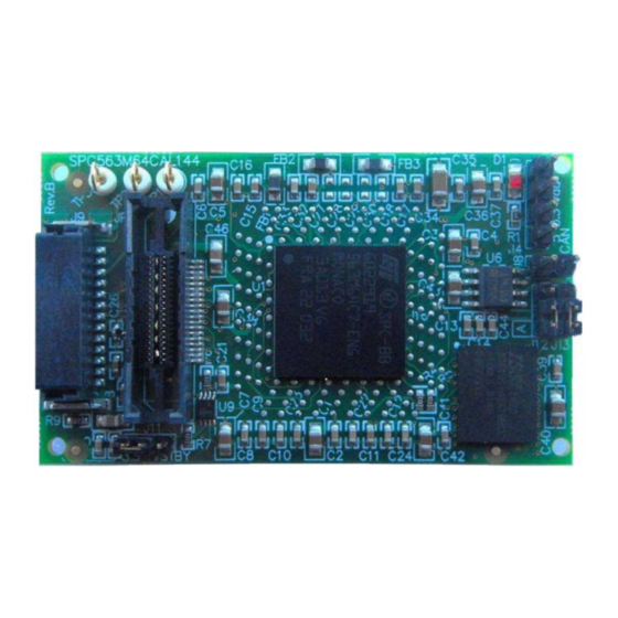
The SPC563M64CAL144 (rev.B) system is designed to enable the use of new enhanced
automotive calibration and debug tools on the SPC563M64xx family of automotive
microcontrollers.
The SPC563M64CAL144 (rev.B) can be fitted onto the application printed circuit board
(PCB) in place of the standard SPC563M64xx family microcontroller in LQFP144 package.
SPC563M64CAL144 (rev.B) hardware is designed to support two standardized tool
connectors, allowing a variety of calibration and debug hardware to be connected and
reused
Figure 1.
Table 1.
SPC563M64CAL144
September 2013
calibration adapter board for SPC563M64xx devices
SPC563M64CAL144 (rev.B)
Board summary
Order code
Doc ID 024080 Rev 3
Reference manual
SPC563M64CAL144
On board device
SPC563M64xx
RM0345
Target footprint
QFP144
1/38
www.st.com
Advertisement
Table of Contents

Related Manuals for ST SPC563M64CAL144


Summary of Contents for ST SPC563M64CAL144
-
Page 1: Table 1. Board Summary
SPC563M64CAL144 calibration adapter board for SPC563M64xx devices Introduction The SPC563M64CAL144 (rev.B) system is designed to enable the use of new enhanced automotive calibration and debug tools on the SPC563M64xx family of automotive microcontrollers. The SPC563M64CAL144 (rev.B) can be fitted onto the application printed circuit board (PCB) in place of the standard SPC563M64xx family microcontroller in LQFP144 package. -
Page 2: Table Of Contents
Contents RM0345 Contents Calibration system overview ........6 Features overview . - Page 3 RM0345 Contents Revision history ........... . 37 Doc ID 024080 Rev 3 3/38...
- Page 4 List of tables RM0345 List of tables Table 1. Board summary ............1 Table 2.
- Page 5 SPC563M64CAL144 (rev.B)........
-
Page 6: Calibration System Overview
Calibration system overview RM0345 Calibration system overview The Calibration Adapter board features 2 Mbytes of SRAM in order to substitute to the SPC563M64xx internal Flash during calibration. A voltage regulator is also integrated upon the board to generate, from selectable 5 V source, the 3.3 V voltage for the RAM and the calibration bus interface. -
Page 7: Power Supply
+3.3 V to supply the SPC563M64xx calibration bus interface and for the external RAM. The 3.3 V supply is generated on the SPC563M64CAL144 (rev.B) via the very low drop voltage regulator by using the +5V. A LED (D1) will light when the board is powered. -
Page 8: Figure 3. Supply Signals From The Qfp144 Footprint
Power supply RM0345 Figure 3. Supply signals from the QFP144 footprint VDDEH1 . A VDDEH1A VDDEH1B VDDEH1B VDDE H1B VDDEH1 C VDDE H 6A VDDEH 4 VDDEH6A VDDEH6A VDDEH6B VDDEH6B VDDEH7 VDDEH7 VDDEH7 Default = CLOSE VDDPLL VDDS YN VDDREG VDDREG Default = CL VRC33... -
Page 9: Figure 5. Supply Signals On Spc563M64Xx Csp496
RM0345 Power supply Figure 5. Supply signals on SPC563M64xx CSP496 The VRC33 signal of the CSP496 is connected to its respective signal of the QFP144 target application via the J15 cut trace option. The VRC33 can be also connected to the on board +3.3V by closing the J2 gauge. In this case the gauge J15 must be open (Table Doc ID 024080 Rev 3... -
Page 10: Table 2. J15, J2 And J14 Option Cut Traces
Power supply RM0345 Table 2. J15, J2 and J14 option cut traces Option Function Value Note name VRC33 signal is disconnected from the target open application board VRC33 close VRC33 signal is connected to the target application board (default) open VRC33 signal is disconnected from the on board +3.3V signal (default) -
Page 11: Reset And Configuration Signals
RM0345 Reset and configuration signals Reset and configuration signals Calibration and debug tools may use the reset signals included in the connectors to have visibility of when the SPC563M64xx device has been reset. Debug tools may also require the ability to force device reset. All signals of the SPC563M64xx QFP144 footprint from the application board are directly connected to the respective calibration device signals. -
Page 12: Calibration Bus Interface And External Memory
Calibration bus interface and External Memory RM0345 Calibration bus interface and External Memory The SPC563M64xx features a 16-bit de-multiplexed calibration bus interface that is connected to an external 2Mbyte SRAM thanks to an on board latch. External memory specification calibration board provides a SRAM with the following characteristics: –... -
Page 13: Table 4. J11 Configuration Of Sram Supply For Retention Mode
RM0345 Calibration bus interface and External Memory Figure 6. SRAM supply circuitry LF33CDT-TRY +3.3V STT5PF20V Vmem 4.7uF 100n 2.2uF 100n Vmem /RSOUT /RESET 74V1G00CTR Vmem /CE_RAM /CS0 74V1G32CTR ECU_Vstby +3.3V 20CJQ060 VSTBY GAPGRI00344 The jumper J11 (see Figure 6) allows to select the standby operation of the SRAM. The standby voltage can be selected between: SPC563M64xx Vstby pin: same standby voltage as the internal RAM;... -
Page 14: Calibration Bus Interface
Calibration bus interface and External Memory RM0345 Calibration bus interface The calibration bus is made up of address bus, data bus, and bus control signals, and is used on the calibration board to access the upon board memory. The calibration board supports a 16-bit de-mulitplexed calibration bus. This is derived from the multiplexed bus on the SPC563M64xx, where the majority of address lines are derived from the data lines (CAL_DATA on SPC563M64 device), by using an onboard external latch controlled by the C_TS signal. -
Page 15: Development Connector
RM0345 Development connector Development connector The JTAG signals and Nexus functionality with 12 Message Data Out (MDO) signals are available on the JP1 development connector (Nexus connector). A hardware control bit in the SPC563M64xx Nexus port controller, is used to control whether the added signals for full width trace port are routed to the MDO[4:11] signals, or the CAL_MDO[4:11] signals. -
Page 16: Table 6. Nexus Signals On Amp 38 Mictor Connector
Development connector RM0345 Figure 6 shows the mapping of the development connector that provides Debug, Nexus trace and calibration signals. The port connector is an AMP 38 pin Mictor style. Figure 9. AMP 38 Mictor Table 6. Nexus signals on AMP 38 Mictor connector Description Descriptio C_MDO9... -
Page 17: Calibration Connector
RM0345 Calibration connector Calibration connector The board is equipped with an ERNI connector to give a more robust solution in terms of physical connectivity for Calibration purpose. Figure 10. J9 Calibration connector Table 7 shows the mapping of the calibration connector that provides Debug and calibration signals. - Page 18 Calibration connector RM0345 Table 7. Nexus signals on AMP 38 Mictor connector (continued) SPC563M64xx SPC563M64xx standard function standard function routing routing GPIO Pins for startup GPIO[207] Detect that the PLL is handshake and MDO 0 (@3.3V) locked triggering VDDP Comparator VDDSBRAM Supply Input (Supply of ECU_Vsby...
-
Page 19: Tool Io
RM0345 Tool IO Tool IO The SPC563M64xx in CSP496 package provides 2 signals, GPIO[206] & GPIO[207], that are not available in the QFP144 standard production package. They can be used by the calibration tools to implement triggers and handshakes. On the calibration board, these signals are available on the JP1 development connector and J9 calibration connector. -
Page 20: Can Interface
CAN interface RM0345 CAN interface calibration board is equipped with one ST L9616 High-Speed Transceiver. It provides the Controller Area Network (CAN) communication interface through the SPC563M64xx CAN interface for calibration via CAN. This serial communication can reach speeds up to 1Mbps. -
Page 21: Table 9. J6, J17 And J7 Flexcan Interface Selection
The cut trace options J6, J17, J18 and J19 has been put in the design of this board to select the supply of the CAN transceiver between 5 V and 3.3 V. By this option is possible to replace the ST L9616 High-Speed Transceiver mounted on board by default, with a different transceiver that operates at 3.3 V. -
Page 22: Calibration Software Compatibility And Configuration
Calibration software compatibility and configuration RM0345 Calibration software compatibility and configuration calibration board uses standard production silicon packaged in the CSP (Chip Scale Package). Therefore, all production silicon features exist and are identical on the calibration board. The required initialization code may be as simple as the configuration of the EBI and its related pins in the SIU, and it could be integrated into standard application software. -
Page 23: Cal Bus Eccr Settings
RM0345 Calibration software compatibility and configuration Table 11. Calibration bus signals configuration (continued) SPC563M64xx signal name Function Notes field mcu signal name Calibration CAL_CS[3] chip select C_CS[3] Calibration CAL_ADDR[11] address bus Calibration C_OE CAL_OE Output enable Calibration C_RD_WR CAL_RD_WR Read/write Calibration C_WE[0:1] CAL_WE[0:1]... -
Page 24: Cal Bus Ebi Settings
Calibration software compatibility and configuration RM0345 9.1.3 Cal Bus EBI Settings For using the calibration bus with an external memory the user must configure the bus for multiplexed operation. These settings are located in two registers: – EBI Module Configuration Register (EBI_MCR) –... -
Page 25: Table 14. Ebi_Cal_Brx Register Setting
RM0345 Calibration software compatibility and configuration Table 14. EBI_CAL_BRx register setting Name Description value field These bits are compared to the corresponding unmasked address signals among ADDR[0:16] of the internal address bus to determine if a memory bank controlled by the memory controller is being accessed by an internal bus master Note: An MCU may have some of the upper bits of the BA field tied to a fixed value internally in order to restrict... -
Page 26: Table 15. Ebi_Cal_Box Register Setting
Calibration software compatibility and configuration RM0345 Table 14. EBI_CAL_BRx register setting Name Description value field The user writes this bit to indicate that the contents of this Base Register and Option Register pair are valid. The appropriate CS signal does not assert unless the corresponding V-bit is set. -
Page 27: Example Configuration Code
RM0345 Calibration software compatibility and configuration Example Configuration CODE The following code is used to configure the calibration bus for 16bit de-multiplexed mode. //--------------------------------------------------- // SIU PCR (Pad Configuration Register) setup // (Cal BUS bommon drive strength = 20pF, DSC = 0b01) //--------------------------------------------------- SIU.PCR[336].R = 0x0040;//CAL_CS[0]DSC=20pF (0b01) SIU.PCR[338].R = 0x0440;//CAL_CS[2] (PA=0b1),DSC=20pF (0b01) - Page 28 Calibration software compatibility and configuration RM0345 //----------------------------------------- // EBI Option Register setup: // Address mask = 0xefe00000; // Wait state = 0 (set 0 wait states); EBI.CAL_CS[0].OR.R = 0xffe00000; 28/38 Doc ID 024080 Rev 3...
-
Page 29: Appendix A Calibration Base Footprints
Calibration base footprints Appendix A Calibration base footprints SPC563M64CAL144 (rev.B) calibration board had footprint compatible with QFP144 production package version of SPC563M64xx devices, ensuring that they can be fitted to an application PCB that has been designed to accept standard QFP144 packaged SPC563M64xx devices. -
Page 30: Appendix B Mechanical Constrains
Mechanical constrains RM0345 Appendix B Mechanical constrains Figure 14. Top and side view drawing 30/38 Doc ID 024080 Rev 3... -
Page 31: Figure 15. Side And Bottom View Drawing
RM0345 Mechanical constrains Figure 15. Side and bottom view drawing Doc ID 024080 Rev 3 31/38... -
Page 32: Figure 16. Complete System Side View Drawing
Mechanical constrains RM0345 Figure 16. Complete system side view drawing 32/38 Doc ID 024080 Rev 3... -
Page 33: Appendix C Schematic
RM0345 Schematic Appendix C Schematic Figure 17. SPC563M64xx in CSP package schematic GAPGRI00355 Doc ID 024080 Rev 3 33/38... -
Page 34: Figure 18. Polypod-Tq144 Connector Schematic
Schematic RM0345 Figure 18. Polypod-TQ144 connector schematic AN.0 EMIOS.0 EMIOS0 AN.1 EMIOS.2 EMIOS2 AN.2 EMIOS.4 EMIOS4 AN.3 EMIOS.8 EMIOS8 AN.4 EMIOS.9 EMIOS9 AN.5 Polypod-TQ144 EMIOS.10 EMIOS10 AN.6 EMIOS.11 EMIOS11 AN.7 EMIOS.12 EMIOS12 AN.9 EMIOS.14 EMIOS14 AN.11 EMIOS.23 AN11 EMIOS23 AN.12 AN12-SDS AN.13 AN13-SDO... -
Page 35: Figure 19. Memory, Can And Connectors Schematic
RM0345 Schematic Figure 19. Memory, CAN and connectors schematic GAPGRI00357 Doc ID 024080 Rev 3 35/38... -
Page 36: Appendix D Options Placement
Options placement RM0345 Appendix D Options placement Figure 20. Options placement TOP view Bottom view GAPGRI00358 36/38 Doc ID 024080 Rev 3... -
Page 37: Table 16. Document Revision History
RM0345 Revision history Revision history Table 16. Document revision history Date Revision Changes 18-Jan-2013 Initial release. 13-Feb-2013 Modified Figure 17-Sep-2013 Updated Disclaimer. Doc ID 024080 Rev 3 37/38... - Page 38 No license, express or implied, by estoppel or otherwise, to any intellectual property rights is granted under this document. If any part of this document refers to any third party products or services it shall not be deemed a license grant by ST for the use of such third party products or services, or any intellectual property contained therein or considered as a warranty covering the use in any manner whatsoever of such third party products or services or any intellectual property contained therein.
Need help?
Do you have a question about the SPC563M64CAL144 and is the answer not in the manual?
Questions and answers