Table of Contents
Advertisement
Advertisement
Table of Contents

Related Manuals for IDEC MICRO3


Summary of Contents for IDEC MICRO3
- Page 1 Micro Programmable Logic Controller User’s Manual...
- Page 2 MICRO • All ’s are manufactured under IDEC’s rigorous quality control system, but users must add a backup or failsafe pro- MICRO vision to the control system using the in applications where heavy damage or personal injury may be caused in...
- Page 3 Under no circumstances shall IDEC Corporation be held liable or responsible for indirect or consequential damages resulting from the use of or the application of IDEC PLC components, individually or in combination with other equipment. All persons using these components must be willing to accept responsibility for choosing the correct component to suit their appli- cation and for choosing an application appropriate for the component, individually or in combination with other equipment.
-
Page 4: Table Of Contents
ABLE OF ONTENTS HAPTER ENERAL NFORMATION Features ............1-1 Parts Description . - Page 5 ABLE OF ONTENTS CPU C (FUN) HAPTER ONFIGURATION FUN Settings (FUN1 through FUN11) ........5-1 FUN Settings (FUN20 through FUN50) .
- Page 6 ABLE OF ONTENTS HAPTER ASIC NSTRUCTIONS Basic Instruction List ..........7-1 LOD (Load) and LODN (Load Not).
- Page 7 ABLE OF ONTENTS HAPTER OOLEAN OMPUTATION NSTRUCTIONS ANDW (AND Word) ......... . . 12-1 ORW (OR Word) .
-
Page 8: General Information
1: G ENERAL NFORMATION Introduction This chapter describes general information for understanding MICRO functions and specifications. Features MICRO is a space-saving micro programmable controller, yet has high-performance functions described below: High-speed Processing Function operates in standard processing mode or high-speed processing mode. Standard mode has a program capacity of MICRO 1012 steps, minimum processing time of 1.2 µsec per basic instruction, and average scan time of 2.9 msec for 1,000 steps. -
Page 9: Parts Description
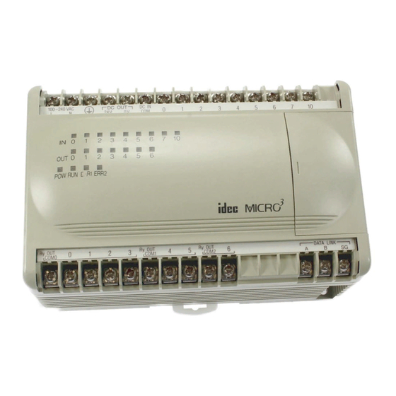
1: G ENERAL NFORMATION Parts Description This section describes parts names and functions of the MICRO base unit. Sensor Power Terminals Input Terminals For supplying power to sensors (24V DC, 150mA). These For connecting input signals from input terminals have an overload sensing function. devices such as sensors, pushbuttons, and limit switches. -
Page 10: System Setup
1: G ENERAL NFORMATION System Setup This section describes settings and precautions for the basic system, expansion system, and various link systems consisting of MICRO Basic System The basic system consists of the base unit and the program loader. This system is used to edit a user program on the pro- gram loader, transfer the user program to the base unit, start and stop the base unit operation, and monitor the operating status. - Page 11 1: G ENERAL NFORMATION Link Systems has three link functions; expansion link, data link, and computer link. When using a link function, the function MICRO selector switch may have to be set or the FUN settings may be required. For details of these settings, see Expansion Link Function on page 4-6, Data Link Function on page 4-8, and Computer Link 1:N Communication on page 4-17.
-
Page 12: General Specifications
1: G ENERAL NFORMATION General Specifications Type AC Power DC Power Rated Power Voltage 100 to 240V AC 24V DC Allowable Voltage 85 to 264V AC 19 to 30V DC (including ripple) Range Between power terminal and FG: Between power terminal and FG: 2000V AC, 1 minute 1500V AC, 1 minute Dielectric Strength... - Page 13 1: G ENERAL NFORMATION General Specifications, continued Operating Temperature 0 to 60°C Storage Temperature –25 to +70°C Relative Humidity Relative humidity severity level RH1, 30 to 95% (non-condensing) Pollution Degree 2 (IEC 664) Corrosion Immunity Free from corrosive gases Operation: 0 to 2,000m (0 to 6,565 feet) Altitude Transport: 0 to 3,000m (0 to 9,840 feet) Vibration Resistance...
-
Page 14: Function Specifications
1: G ENERAL NFORMATION Function Specifications Mode Standard Processing High-speed Processing Program Capacity 1012 steps Approx. 100 steps User Program Memory EEPROM, RAM (backed up by battery) A user program is transferred from the program loader through the CPU to RAM and EEPROM in the MICRO . - Page 15 1: G ENERAL NFORMATION Function Specifications, continued Mode Standard Processing High-speed Processing Points/Phase 1 point, single-phase HSC0, HSC1, HSC2: 0 to 4,294,967,295 High-speed Preset Value HSC3: 0 to 65535 Counter HSC0 and HSC3: 10 kHz Frequency Response HSC1 and HSC2: 5 kHz Pulse Output 1 channel (available on transistor output types only)
-
Page 16: Communication And Noise Specifications
1: G ENERAL NFORMATION Communication and Noise Specifications Loader Port Communication Specifications For the MICRO , see the MICRO User’s Manual. C specifications Standards EIA RS485 (termination resistor is not required) Connection to Program Loader Using optional loader cable (FC2A-KL1 or FC2A-KL2) 1:1 Communication Using optional computer link cable FC2A-KC2 1:N Communication... - Page 17 1: G ENERAL NFORMATION Power Supply Timing Chart Turn on AC or DC main power and I/O power at the same time, or turn on AC or DC main power first. Turn off AC or DC main power and I/O power at the same time, or turn off I/O power first. AC/DC Main Power I/O Power ≥...
-
Page 18: Digital Dc Input Specifications
1: G ENERAL NFORMATION Digital DC Input Specifications Rated Input Voltage 24V DC sink/source input signal Input Voltage Range 19 to 30V DC I0 and I20: 2.1 kΩ Input Impedance I1 to I15, I21 to I35: 3.5 kΩ 4 µsec + filter preset Turn ON Time I1 to I15: 20 µsec + filter preset... - Page 19 1: G ENERAL NFORMATION Input Operating Range Digital DC Input Digital AC Input Input I1-I15 Impedance Input I0 Impedance Input Impedance 132V ON Area ON Area Transition Area Transition Area OFF Area OFF Area 1.2mA 14mA 10mA 2.5mA Input Current Input Current Input Internal Circuit Digital DC Input...
-
Page 20: Digital Ac/Dc Output (Relay Output) Specifications
1: G ENERAL NFORMATION Digital AC/DC Output (Relay Output) Specifications I/O Type 10-I/O Type 16-I/O Type 24-I/O Type Output Protection Without protection Protection Circuits Prepared by User See page 1-17. Output Points 4 points 7 points 10 points Common NO COM0 Common NO 4 points 3 points... -
Page 21: Digital Dc Output (Transistor Sink Output) Specifications
1: G ENERAL NFORMATION Digital DC Output (Transistor Sink Output) Specifications I/O Type 10-I/O Type 16-I/O Type 24-I/O Type Output Protection Without protection Protection Circuits Prepared by User See page 1-23. Output Points 4 points 7 points 10 points COM0 4 points 4 points 5 points... -
Page 22: Digital Dc Output (Transistor Protect Source Output) Specifications
1: G ENERAL NFORMATION Digital DC Output (Transistor Protect Source Output) Specifications I/O Type 10-I/O Type 16-I/O Type 24-I/O Type Output Protection Protected output Output Points 4 points 7 points 10 points COM0 4 points 4 points 5 points Output Points per Common Line COM1 —... - Page 23 1: G ENERAL NFORMATION Output Delay Digital AC/DC Output (Relay Output) Command Output Status OFF delay: 10 msec maximum Chatter: 6 msec maximum ON delay: 6 msec maximum Digital DC Output (Transistor Sink Output) Command Test Condition: Load resistance 1 kΩ 24V DC Output Status OFF delay Q0:...
- Page 24 1: G ENERAL NFORMATION Contact Protection Circuit for Relay Output Depending on the load, a protection circuit may be needed for the relay output of the MICRO . Choose a protection circuit from A through D shown below according to the power supply and connect the protection circuit to the outside of the MICRO Protection Circuit A This protection circuit can be used when the load impedance is...
-
Page 25: Program Loader Specifications
1: G ENERAL NFORMATION Program Loader Specifications • Supplied by the MICRO base unit through the loader cable. • Supplied by an AC adapter during off-line programming. Applicable AC adapter 5 to 6.5 V DC, 4W Output plug: Power Supply Polarity ø2.1 –... -
Page 26: Input Terminal Arrangements
1: G ENERAL NFORMATION Input Terminal Arrangements DC Input (AC Power Type) 10-I/O Unit (6 inputs) 100-240V AC DC OUT DC IN 16-I/O Unit (9 inputs) 100-240V AC DC OUT DC IN 24-I/O Unit (14 inputs) 100-240V AC DC OUT DC IN AC Input (AC Power Type) 16-I/O Unit... -
Page 27: Output Terminal Arrangements
1: G ENERAL NFORMATION Output Terminal Arrangements Relay Output (DC Input Type) Ry. OUT Ry. OUT DATA LINK 10-I/O Unit COM0 COM1 (4 outputs) Ry. OUT Ry. OUT Ry. OUT DATA LINK 16-I/O Unit COM0 COM1 COM2 (7 outputs) Ry. OUT Ry. -
Page 28: Input Wiring Diagrams
1: G ENERAL NFORMATION Input Wiring Diagrams • Emergency and interlocking circuits must be configured outside the . If such a circuit is MICRO Warning configured inside the , failure of the may cause disorder of the control system, MICRO MICRO damage, or accidents. - Page 29 1: G ENERAL NFORMATION Input Wiring Diagrams, continued DC Sink Input (AC Power Type) • When using the sensor power supply from the DC OUT terminals 100-240V AC 2-wire Ground Main Power Sensor Transistor Sensor Switch – 3A Fuse 100-240V AC DC OUT DC IN •...
-
Page 30: Output Wiring Diagrams
1: G ENERAL NFORMATION Output Wiring Diagrams Relay Output Ry. OUT Ry. OUT Ry. OUT DATA LINK COM0 COM1 COM2 External Power 240V AC/30V DC 2A × Output Point Fuse – Fuse – : Insert proper fuses depending on the load. Fuse –... -
Page 31: Dimensions
1: G ENERAL NFORMATION Dimensions MICRO Base Unit Program Loader 30 mm (1.181") 95 mm (3.740") 10-I/O Type: 105 mm (4.134") 60 mm (2.362") 16-I/O Type: 135 mm (5.315") 24-I/O Type: 165 mm (6.496") AC Input Type: 165 mm (6.496") Mounting Hole Layout for MICRO Base Units 80 mm (3.150") -
Page 32: Installation
1: G ENERAL NFORMATION Installation This section describes the methods and precautions for installing the MICRO • Turn power off to the before starting installation, removal, wiring, maintenance, and MICRO Warning inspection on the . Failure to turn power off may cause electrical shocks or fire hazard. MICRO •... -
Page 33: Disposing Of The Micro Units
NFORMATION DIN Rail Mounting The MICRO unit can be mounted on a 35-mm-wide DIN rail. Applicable DIN rail: IDEC’s BAA1000 (1000mm/39.4" long) • Mounting on DIN Rail Unit Groove Fasten the DIN rail to a panel using screws firmly. Put the groove of the MICRO base unit on the DIN rail, with the input ter- minal side up, and press the unit to the panel as shown on the right. -
Page 34: Wiring
1: G ENERAL NFORMATION Wiring • Use wires of a proper size to meet voltage and current requirements. Tighten M3 screws for power Caution and I/O terminals to a proper tightening torque of 0.3 to 0.5 N-m. • Do not disassemble, repair, or modify the MICRO Power Supply Wiring Use a stranded wire of 1.25 mm... - Page 35 1: G ENERAL NFORMATION Power Supply Voltage • Use a power supply of the rated value. Use of a wrong power supply may cause fire hazard. Caution • Use an IEC127-approved fuse on the power line outside the . This is required when MICRO exporting equipment containing to Europe.
-
Page 36: Operation Basics
2: O PERATION ASICS Introduction This chapter describes general information for starting and stopping MICRO operation, and introduces simple operating procedures from creating a user program to monitoring the MICRO operation. • Make sure of safety before starting and stopping the or when operating the MICRO MICRO... - Page 37 2: O PERATION ASICS Start/Stop Operation using the Power Supply can be started and stopped by turning power on and off. MICRO 100-240V AC DC OUT DC IN Check that start control special internal relay M300 is on using the pro- gram loader.
-
Page 38: Simple Operation
2: O PERATION ASICS Simple Operation This section describes how to edit a simple program using the program loader connected to MICRO , transfer the program to MICRO , run the program on MICRO , and monitor the operation on the program loader. Connect Program Loader to MICRO Connect the program loader to MICRO... -
Page 39: Program Loader
2: O PERATION ASICS Create a User Program Create a simple program using the program loader. The sample program performs the following operation: When input I0 is turned on, output Q0 is maintained. When input I1 is turned on, output Q1 is maintained. When input I2 is turned on, both outputs Q0 and Q1 are reset. - Page 40 2: O PERATION ASICS Transfer Program and Monitor Operation MICRO Transfer the program to the MICRO base unit, run the program and monitor the operation using the program loader using the following procedures. Press the TRS key on the program loader to select the transfer mode. 1Kstep The program loader displays as shown on the right: Loader••••PC...
- Page 41 2: O PERATION ASICS ’ ANUAL...
-
Page 42: Parts Description
3: P ROGRAM OADER Introduction This chapter describes general information for understanding the functions and specifications of the FC2A-HL1E program loader. The program loader is used to edit user programs, transfer a user program to the MICRO base unit, and monitor the operation. - Page 43 3: P ROGRAM OADER Function Keys Clear key used to return to the previous opera- Advance instruction key used to program advanced tion level or back to the editor mode. instructions, to monitor high-speed counter, or to monitor double-word data. Insert key used to insert a program instruction.
-
Page 44: Program Loader Operation Modes
3: P ROGRAM OADER Program Loader Operation Modes The program loader has four operation modes and displays as shown below. Editor Mode The editor mode is used to edit a user program in the user program memory of the 0 LOD program loader. -
Page 45: Programming Procedures And Precautions
3: P ROGRAM OADER Programming Procedures and Precautions This section describes the programming procedures using the program loader. Supply Power The program loader can be powered in two ways. When the program loader is connected to the MICRO base unit using the loader cable, the program loader is powered by the base unit. -
Page 46: Using Editor Mode
3: P ROGRAM OADER Using Editor Mode The editor mode is used to create and revise user programs by writing, deleting, and inserting program instructions in the internal RAM (program memory) of the program loader. The display can be scrolled and a selected program instruction or address can be searched for in the editor mode. - Page 47 3: P ROGRAM OADER Entering Program Instructions Program instructions are entered to the program memory at the selected address in the program loader. A new program instruction overwrites the existing program instruction at the selected address. Move the cursor where you want to enter a program instruction using the keys.
- Page 48 3: P ROGRAM OADER Inserting Program Instructions A program instruction can be inserted at any address. When a program instruction is inserted, subsequent program instruc- tions are shifted down. Move the cursor to the address where you want to insert a program instruction. Press the INS key.
- Page 49 3: P ROGRAM OADER Searching for a Program Instruction A specified program instruction can be searched for through the user program. Enter an instruction to search for and start the search by pressing the appropriate key. Searches to the smaller address starting at the cursor position. Searches to the larger address starting at the cursor position.
-
Page 50: Using Transfer Mode
3: P ROGRAM OADER Using Transfer Mode User programs can be transferred between the program loader and the MICRO base unit or the memory card installed in the program loader. The transfer mode includes writing, reading, and comparing of user programs. When the user program in the MICRO base unit is protected from writing and/or reading, the program transfer operation cannot be performed. - Page 51 3: P ROGRAM OADER Writing Program from Program Loader to Memory Card A new memory card must be formatted before writing user programs using FUN41. See “FUN41: Memory Card Format- ting” on page 15. Insert a formatted memory card into the program loader. Make sure that the write protect switch on the memory card is set to the write enable side.
- Page 52 3: P ROGRAM OADER Comparing Programs between Program Loader and Memory Card Insert a memory card containing user programs into the program loader. Press the keys: 1Kstep (Verify) Loader Card 1:PROGRAM1 Select a program name in the memory card as described on the preceding page and start the program comparison by pressing the keys: 1Kstep (Verify)
-
Page 53: Using Monitor Mode
3: P ROGRAM OADER Using Monitor Mode The monitoring mode is enabled by pressing the MON key on the program loader. The statuses of inputs, outputs, internal relays, shift registers, the preset and current values of timers and counters, and the data of data registers can be monitored on the program loader. - Page 54 3: P ROGRAM OADER Monitoring Timers and Counters The preset and current values of timers and counters are displayed. Press the MON key to enable the monitor mode. Enter the operand and number to monitor. Press the key to start monitoring. Example: Monitor timer T10 To enable the monitor mode, press the key: Enter the operand and number to monitor:...
- Page 55 3: P ROGRAM OADER Changing Preset Values for Timers and Counters Preset values for timers (TIM, TMH, and TMS) and counters can be changed by transferring a new value to the MICRO base unit RAM. This is possible whether the base unit is running or not. Only preset values programmed with a constant value can be changed using a constant value by this operation.
- Page 56 3: P ROGRAM OADER Monitoring High-speed Counters The preset and current values of high-speed counters HSC0 through HSC3 are displayed in decimal or hexadecimal nota- tion on the program loader. Press the MON key to enable the monitor mode. Enter the CNT and ADV keys, followed by the operand number 0 through 3 to monitor. Press the LOD/10 or OUT/16 key to display the preset or current value in decimal or hexadecimal notation.
- Page 57 3: P ROGRAM OADER Entering Data into Data Registers Data in data registers can be changed using the program loader whether the MICRO base unit is running or not. Data reg- ister values can be entered in decimal or hexadecimal notation. In addition, a double-word value can also be entered into two consecutive data registers in decimal or hexadecimal notation.
- Page 58 3: P ROGRAM OADER Monitoring Data Registers The data of data registers can be displayed in decimal or hexadecimal notation on the program loader. In addition, the dou- ble-word data of two consecutive data registers can also be displayed in decimal or hexadecimal notation. This function is particularly useful for confirming the preset value of high-speed counters when data registers are used for a preset value.
- Page 59 3: P ROGRAM OADER Setting and Resetting • Make sure of safety when operating the to force outputs on (SET) or off (RST). Incorrect MICRO Caution operation on the may cause machine damage or accidents. MICRO Inputs, outputs, internal relays, and shift register bits can be temporarily turned on (SET) or turned off (RST), using the program loader.
- Page 60 3: P ROGRAM OADER Time Chart for SET and RST Operation END Instruction END Instruction END Instruction Actual Actual Actual Actual Actual Actual SET I1 Output Input SET/RST OUT Q1 Output Input SET/RST OUT Q1 Output Input SET/RST Instruction Entered Processed Processed Processed...
-
Page 61: Error Messages For Program Loader Operation
3: P ROGRAM OADER Error Messages for Program Loader Operation When using the program loader for programming or transferring a user program, the following error messages may be displayed. Error Message Error Details Calendar NG Invalid calendar data. CRC Code NG The CRC code of the user program to be transferred is incorrect. -
Page 62: Special Functions
4: S PECIAL UNCTIONS Introduction features special functions such as the high-speed processing mode, catch input function, input filter function, MICRO pulse output function, high-speed counter function, expansion and data link functions, external analog timer function, and analog I/O functions. This chapter describes these special functions. High-speed Processing Mode MICRO can execute the user program in the standard processing mode and the high-speed processing mode. -
Page 63: Catch Input Function
4: S PECIAL UNCTIONS Catch Input Function The catch input function is used to receive short pulses from sensor outputs regardless of the scan time. Since input signals to inputs I0 through I7 are always set to special internal relays M290 through M297, input signals are securely received even if short-pulse input signals turn on and off within one scan time. -
Page 64: Input Filter Function
4: S PECIAL UNCTIONS Example: Counting Catch Input Pulses This example demonstrates a program to count short pulses using the catch input function. Input I1 is used as a reset input for adding counter C2. Reset Input I0 is assigned to catch input special internal relay M290. Counter C2 counts short-pulse inputs to input I0. - Page 65 4: S PECIAL UNCTIONS Setting Input Filter Use FUN7 on the program loader to set the hard filter and soft filter values. See page 5-6. Hard filter: 0 through 255 (default value is 10) Input I0 ON pulse = 4 to 616 µsec, Input I0 OFF pulse = 6 to 618 µsec Inputs I1 to I7 ON pulse = 20 to 625 µsec, Inputs I1 to I7 OFF pulse = 120 to 618 µsec Soft filter: 0, 3, 7, or 10 msec (default value is 3 msec)
-
Page 66: Pulse Output Function
4: S PECIAL UNCTIONS Example: Receiving Minimum Pulse Width of 150 µsec When input I0 is required to receive short pulses of 150 µsec minimum using the catch input function, the preset value N for the hard filter is calculated as follows. From Equation A on page 4-4, 150 = 2.4N + 4 N = 60.8 Set the hard filter preset value N to 60 or less to catch short input ON pulses of 150 µsec. -
Page 67: Expansion Link Function
4: S PECIAL UNCTIONS Expansion Link Function I/O points can be expanded by connecting another MICRO base unit using a shielded 2-core twisted cable. Only one unit can be added to expand I/O points from 10, 16, or 20 points up to 48 points. The expansion link function cannot be used with the data link function or in the high-speed processing mode. - Page 68 4: S PECIAL UNCTIONS I/O Allocation Numbers for Expansion Link System Input and output allocation numbers do not continue from the base station to the expansion station. At the expansion sta- tion, inputs start at I20 and outputs start at Q20. Inputs and outputs are allocated depending on the MICRO base units used in the expansion link system as shown below: I/O Points...
-
Page 69: Data Link Function
4: S PECIAL UNCTIONS Data Link Function MICRO features the data link function to set up a distributed control system. A maximum of six slave stations can be con- nected to the master station. Data of inputs, outputs, internal relays, timers, counters, shift registers, and data registers are communicated between the master and slave stations. - Page 70 4: S PECIAL UNCTIONS Data Link Specifications Electric Specifications Compliance with EIA-RS485 Baud Rate 19200 bps (fixed) Maximum Cable Length 200m (656 feet) total Maximum Slave Stations 6 slave stations Communication Sequence Only one slave station can communicate with the master station in one scan. When a slave station receives a command from the master station, the slave station returns a response of processing results.
- Page 71 4: S PECIAL UNCTIONS Operating Procedure for Data Link System To set up and use a data link system, complete the following steps: First determine the assignments for the master station and slave stations. Connect MICRO base units at the master station and all slave stations as illustrated on page 4-8. Set the function selector switch to 0 on the MICRO base unit at the master station and to 1 through 6 at slave stations.
- Page 72 4: S PECIAL UNCTIONS Data Link Example 2: Data Transmission from Slave Station This sample program demonstrates data communication from slave station 1 to the master station, then to slave station 2. Data of inputs I0 through I7 and I10 through I17 are set to data register D86 (transmission data H) at slave station 1. The D86 data is sent to data register D63 (receive data H for slave station 1) of the master station.
- Page 73 4: S PECIAL UNCTIONS Data Link Example 3: Input and Counter Data Transmission, continued Master Station Slave Station 1 D60 (Error Code) D85 (Error Code) I0 through I7, I10 through I17 D61 (Trans. H) D86 (Trans. H) Counter C2 current value D62 (Trans.
- Page 74 4: S PECIAL UNCTIONS Data Link Example 4: Data Transmission through FA-3S Serial Interface Module This sample program demonstrates data communication between the FA-3S master station and MICRO slave stations using the PF3S-SIF4 serial interface module. FA-3S series high-performance CPU module PF3S-CP12 or PF3S-CP13 is used for the master station.
- Page 75 4: S PECIAL UNCTIONS Data Link Example 4: Data Transmission through FA-3S Serial Interface, continued Data movement and LCOPR (local operand) has two data registers for transmission and two data registers for receiving in the data link system. So, each MICRO slave station can communicate four words of data with the FA-3S master station.
- Page 76 4: S PECIAL UNCTIONS Data Link Example 4: Data Transmission through FA-3S Serial Interface, continued Master station program for FA-3S high-performance CPU (IS-NET communication universal mode) M304 is the initialize pulse special inter- nal relay. WNSET cN-W When the CPU starts, local operand data is M304 DR+0 DR+1...
-
Page 77: Computer Link Function
4: S PECIAL UNCTIONS Computer Link Function A personal computer can be connected to one MICRO base unit in a peer-to-peer configuration (1:1 communication) or to a maximum of 32 MICRO base units in a network configuration (1:N communication). Using the optional software CUBIQ (FC9Y-LP1E314) on an IBM PC or compatible, user programs can be edited on the computer and transferred between the computer and MICRO . - Page 78 4: S PECIAL UNCTIONS Computer Link 1:N Communication To set up a 1:N computer link system, connect a computer to RS232C/RS485 converter using RS232C cable HD9Z-C52. Connect the RS232C/RS485 converter to computer link interface units FC2A-LC1 using shielded twisted pair cables. Connect MICRO to each computer link interface unit using computer link interface cable FC2A-KC3.
-
Page 79: External Analog Timer
4: S PECIAL UNCTIONS External Analog Timer Analog timer unit PFA-1U11 can be connected to MICRO to be used as an external analog timer and the preset value can be adjusted in very small increments from the panel front. Analog Timer Unit PFA-1U11 The analog timer unit generates output pulses of approximately 80 msec and the interval can be changed between 20 msec and 2 sec using the knob on the analog timer unit. - Page 80 4: S PECIAL UNCTIONS Example: ON-delay Analog Timer This example demonstrates a program to vary the timer preset value for the TIM instruction between 0.2 and 20 sec using the TMH instruction for measuring the output pulse OFF duration of the external analog timer unit. Start input for TIM1 Input I0 Pulse output from the external analog timer unit...
- Page 81 4: S PECIAL UNCTIONS Analog Timer Unit and Accessories Name Type No. Remarks Analog Timer Unit PFA-1U11 For changing the preset value of timer instructions DIN Rail Mount Socket SR2P-06U With screw terminals SR2P-511 With solder terminals Panel Mount Socket SR2P-70 With wire wrap terminals Panel Mount Adapter...
-
Page 82: Analog Input Function
4: S PECIAL UNCTIONS Analog Input Function The A/D converter unit is used with MICRO to perform an 8-bit A/D conversion. The A/D converter unit reads analog input signals from an analog output device such as an analog distance sensor. The output from the A/D converter unit is entered to MICRO input I0 and converted into a digital value 0 through 249 using the A/D (analog/digital conversion) instruction. - Page 83 4: S PECIAL UNCTIONS General Specifications (A/D Converter Unit) Rated Power Voltage 24V DC Allowable Voltage Range 19 to 30V DC (including ripple) Between input and output terminals: 500V AC Dielectric Strength Between I/O terminal and FG: 1500V AC Between power and output terminals: Not isolated 10 M Ω...
- Page 84 4: S PECIAL UNCTIONS Function Specifications (A/D Converter Unit) Voltage input unit: 1 MΩ minimum Load Impedance in Signal Range Current input unit: 250Ω Maximum error at 25°C: ±0.6% of full scale Analog Input Error Temperature coefficient: +0.012% of full scale/°C (typ.) Maximum Error over Full Temperature Range ±1% of full scale Digital Resolution...
- Page 85 4: S PECIAL UNCTIONS Power Supply Timing Chart Power up the A/D converter unit and MICRO MICRO Main Power at the same time, or power up the MICRO first. Power down the A/D converter unit and A/D Converter Power at the same time, or power down the MICRO ≥...
- Page 86 4: S PECIAL UNCTIONS Wiring Diagram • Source Input to MICRO 24V DC – Power 3A Fuse When using the MICRO in the source input connection, select the sink out- put from the A/D converter unit. – 24V DC Set the output selector A/D UNIT switch to SINK.
- Page 87 4: S PECIAL UNCTIONS Example: A/D Conversion The following example demonstrates a program to perform ON/OFF control on a heater using the A/D converter unit (4 to 20 mA). The temperature sensor generates an analog output of 4 through 20 mA while the temperature changes from 0°C through 100°C.
-
Page 88: Analog Output Function
4: S PECIAL UNCTIONS Analog Output Function The D/A converter unit is used with the transistor output type MICRO base unit to perform an 8-bit D/A conversion. The PWM (pulse width modulation) instruction is used to convert the digital value to a pulse output signal. The output from MICRO output Q0 is entered to the D/A converter unit to generate an analog current or voltage output to control an inverter. - Page 89 4: S PECIAL UNCTIONS General Specifications (D/A Converter Unit) Rated Power Voltage 24V DC Allowable Voltage Range 19 to 30V DC (including ripple) Between input and output terminals: 500V AC Dielectric Strength Between I/O terminal and FG: 1500V AC Between power and output terminals: Not isolated 10 M Ω...
- Page 90 4: S PECIAL UNCTIONS Function Specifications (D/A Converter Unit) Voltage output unit: 5 kΩ minimum Load Impedance in Signal Range Current output unit: 250Ω (300Ω maximum) Maximum error at 25°C: ±0.7% of full scale Analog Output Error Temperature coefficient: –0.005% of full scale/°C (typ.) Maximum Error over Full Temperature Range ±1% of full scale Digital Resolution...
- Page 91 4: S PECIAL UNCTIONS Power Supply Timing Chart Power up the D/A converter unit and MICRO MICRO Main Power at the same time, or power up the MICRO first. Power down the D/A converter unit and D/A Converter Power at the same time, or power down the MICRO ≥...
- Page 92 4: S PECIAL UNCTIONS Type of Protection • Input Circuit • Output Circuit The input selector switch is used to Voltage Output Current Output select sink or source input. INPUT 1.5kΩ Photo ANALOG Isolator OUTPUT + 4.7kΩ ANALOG ANALOG +24V DC OUTPUT + 4.7kΩ...
- Page 93 4: S PECIAL UNCTIONS Example: D/A Conversion The following example demonstrates a program to control motor speed using the D/A converter unit. Analog potentiome- ter 0 on the MICRO base unit is used to change the digital value for operand S1 (pulse width coefficient) of the PWM (pulse width modulation) instruction.
-
Page 94: (Fun)
5: CPU C (FUN) ONFIGURATION Introduction This chapter describes setting the FUN (function) table. FUN1 through FUN11 are used to configure the user program and these settings must be designated before attempting to transfer the user program to the MICRO base unit. -
Page 95: Fun Settings (Fun20 Through Fun50)
5: CPU C (FUN) ONFIGURATION FUN Settings (FUN20 through FUN50) Number Name Function PLC error data readout and Displays the error code and data of the MICRO , and clears the FUN20 reset error data. Timer/counter preset value Reads changed timer/counter preset values from MICRO FUN21 readout and restore Restores the original timer/counter preset values. -
Page 96: Key Operation
5: CPU C (FUN) ONFIGURATION Key Operation Each FUN setting screen can be called directly or from a FUN menu. To directly call an individual FUN setting screen, press the FUN key, then enter a FUN number, and press the key as described in detail in the following sections. -
Page 97: Fun2: Reset Input Number Selection
5: CPU C (FUN) ONFIGURATION FUN2: Reset Input Number Selection FUN2 is provided to designate an input number as a reset terminal. When this input is turned on, MICRO stops operation and resets all statuses. See page 2-2 for detailed information on system status during reset. To set FUN2: RESET RESET CC>=... -
Page 98: Fun4: Shift Register "Keep" Designation
5: CPU C (FUN) ONFIGURATION FUN4: Shift Register “Keep” Designation The status of any shift register bit from R0 through R63 is normally cleared during a power failure. It is possible to main- tain the status of a shift register bit by using FUN4 to designate the shift register bit as a “keep” type. The “keep”... -
Page 99: Fun6: Rising Or Falling Edge Selection For Catch Inputs
5: CPU C (FUN) ONFIGURATION FUN6: Rising or Falling Edge Selection for Catch Inputs FUN6 is provided to select whether catch inputs are accepted at the rising (ON pulse) or falling edge (OFF pulse). The catch input signals entered to inputs I0 through I7 are stored to special internal relays M290 through M297. See page 4-2. The edge selection is done in 4 groups of catch inputs: Catch Group I4 through I7 (16- and 24-I/O MICRO... -
Page 100: Fun8: Loader Port Communication Mode Setting
5: CPU C (FUN) ONFIGURATION FUN8: Loader Port Communication Mode Setting The MICRO or MICRO base unit can communicate with a personal computer or modem through the RS485 loader port ( MICRO ) or the RS232C loader port ( MICRO ). -
Page 101: Fun10: Control Data Register Setting
5: CPU C (FUN) ONFIGURATION FUN10: Control Data Register Setting FUN10 is used to select whether data registers D90 through D99 are enabled as a control data register or not. When the control data register function is enabled, the data register stores various data as shown below. Control data registers are for readout only and can be used in the user program or for monitoring. -
Page 102: Fun11: Program Capacity And Plc Type Selection
5: CPU C (FUN) ONFIGURATION FUN11: Program Capacity and PLC Type Selection The user program capacity can be selected from 244, 500, or 1K steps using FUN11: FUN 11 SIZE Program Capacity 1K(step) Program capacity (must be set to 244, 500, or 1K) PLC type code (must be set to 0 or 1) 0: MICRO FUN 11... -
Page 103: Fun22: User Program Protection
5: CPU C (FUN) ONFIGURATION FUN22: User Program Protection The user program in the MICRO base unit can be protected from reading, writing, or both using FUN22. • When proceeding with the following steps, make sure to note the password, which is needed to Warning cancel the program protection. -
Page 104: Fun25: Scan Time Readout
5: CPU C (FUN) ONFIGURATION FUN25: Scan Time Readout The scan time of the user program in the MICRO base unit can be read using FUN25. The current value of the scan time is displayed in units of msec and updated periodically. The maximum value of the scan time is shown in parentheses on the bottom line. -
Page 105: Fun28: Calendar/Clock Data Readout And Setting
5: CPU C (FUN) ONFIGURATION FUN28: Calendar/Clock Data Readout and Setting The calendar/clock data in the 16- and 24-I/O type MICRO base units can be read and changed using FUN 28 CALENDAR FUN28. MCS/R Y:’97 M: 3 D: 4 H:17 M:15 S:34 The calendar/clock data is displayed. -
Page 106: Fun31: Program Loader Version Readout/Hardware Check
5: CPU C (FUN) ONFIGURATION FUN31: Program Loader Version Readout/Hardware Check At the beginning of the hardware check, using FUN31, the version of the program loader system program is displayed. Next, the program loader display is tested, and the internal memory is checked by testing the readout and writing functions of the entire RAM of the program loader. -
Page 107: Fun34: Program Loader Beep Sound
5: CPU C (FUN) ONFIGURATION FUN34: Program Loader Beep Sound The program loader usually beeps to acknowledge FUN 34 BUZZER each key input and signal an error. The buzzer can also be silenced using FUN34. Buzzer Buzzer beeps OFF: Buzzer silenced To return to the editor mode, press the CLR key. -
Page 108: Fun40: Memory Card Identification
After calling the FUN41 screen, move down the cur- FUN 41 FORMAT sor to the colon and enter a card name of 8 characters maximum. Name (IDEC Applicable characters are A through Z, 0 through 9, Card Format OK? and a space. FUN 41... -
Page 109: Fun43: Program Loader System Program Restore
5: CPU C (FUN) ONFIGURATION FUN43: Program Loader System Program Restore The new system program installed using FUN42 can FUN 43 SYS-CLR be cleared, and the original system program of the Extension program loader can be restored using FUN43. System Clear After calling the FUN43 screen, press the key to... -
Page 110: Numbers
6: A LLOCATION UMBERS Introduction For the MICRO , see the MICRO User’s Manual. This chapter describes allocation numbers available for the MICRO base unit to program basic and advanced instructions. Special internal relays are also described. The MICRO programmable controller is programmed using operands such as inputs, outputs, internal relays, timers, counters, shift registers, and data registers. -
Page 111: Special Internal Relays
6: A LLOCATION UMBERS Special Internal Relays Internal relays M290 through M317 are special internal relays with the following functions: Allocation Number Description CPU Stopped Power OFF M290 Input I0 Operating Cleared M291 Input I1 Operating Cleared M292 Input I2 Operating Cleared M293... - Page 112 6: A LLOCATION UMBERS M303 Carry (Cy) and Borrow (Bw) When a carry or borrow results from executing an addition or subtraction instruction, M303 turns on. M303 is also used for the bit shift and rotate instructions. See pages 11-1 and 13-1. M304 User Program Execution Error When an error occurs during executing a user program, M304 turns on.
-
Page 113: Data Register Allocation Numbers
6: A LLOCATION UMBERS M315 High-speed Counter Soft Reset When M315 is turned on while a high-speed counter (HSC0, HSC1, HSC2, or HSC3) is used, the high-speed counter cur- rent value is reset to zero. When M315 is turned off, the high-speed counter restarts to count. M316 High-speed Counter (HSC3) Overflow When the current value of high-speed counter HSC3 exceeds the maximum value of 65535, M316 is turned on. -
Page 114: Basic Instructions
7: B ASIC NSTRUCTIONS Introduction This chapter describes programming of the basic instructions, available operands, and sample programs. Basic Instruction List Addresses Symbol Name Function Required Series connection of NO contact AND LOD And Load Series connection of circuit blocks ANDN And Not Series connection of NC contact... -
Page 115: Lod (Load) And Lodn (Load Not)
7: B ASIC NSTRUCTIONS LOD (Load) and LODN (Load Not) The LOD or LODN instruction is used before an operand starting at the left bus of the ladder diagram. The LOD instruc- tion starts the logical operation with an NO (normally open) contact. The LODN instruction starts the logical operation with an NC (normally closed) contact. - Page 116 7: B ASIC NSTRUCTIONS Examples: LOD (Load), NOT, and OUT (Output) Ladder Diagram Program List Key Operation Prgm Adrs Instruction Data LOD NOT OUT NOT Timing Chart Ladder Diagram Program List Key Operation Prgm Adrs Instruction Data Ladder Diagram Program List Key Operation Prgm Adrs Instruction...
-
Page 117: And And Andn (And Not)
7: B ASIC NSTRUCTIONS AND and ANDN (And Not) The AND instruction is used for programming an NO contact in series. The ANDN instruction is used for programming an NC contact in series. The AND or ANDN instruction is entered after the first set of contacts. Ladder Diagram Valid Operands (Standard Processing) Program List... -
Page 118: And Lod (Load)
7: B ASIC NSTRUCTIONS AND LOD (Load) The AND LOD instruction is used to connect, in series, two or more circuits starting with the LOD instruction. The AND LOD instruction is the equivalent of a “node” on a ladder diagram. The AND LOD instruction is keyed after entering those circuits to be connected. - Page 119 7: B ASIC NSTRUCTIONS Example: AND LOD (Load) For the following circuit, the AND LOD instruction can be used in two ways. First, the AND LOD instruction can be keyed following each of the sets of circuits that Ladder Diagram are to be connected in series.
-
Page 120: Or Lod (Load)
7: B ASIC NSTRUCTIONS OR LOD (Load) The OR LOD instruction is used to connect, in parallel, two or more circuits starting with the LOD instruction. The OR LOD instruction is the equivalent of a “node” on a ladder diagram. The OR LOD instruction is keyed after entering those circuits to be connected. - Page 121 7: B ASIC NSTRUCTIONS Example: OR LOD (Load) For the following circuit, the OR LOD instruction can be used in two ways. Ladder Diagram First, the OR LOD instruction can be keyed following each of the sets of circuits that are to be connected in parallel.
-
Page 122: Bps (Bit Push), Brd (Bit Read), And Bpp (Bit Pop)
7: B ASIC NSTRUCTIONS BPS (Bit Push), BRD (Bit Read), and BPP (Bit Pop) The BPS (bit push) instruction is used to save the result of bit logical operation temporarily. The BRD (bit read) instruction is used to read the result of bit logical operation which was saved temporarily. The BPP (bit pop) instruction is used to restore the result of bit logical operation which was saved temporarily. - Page 123 7: B ASIC NSTRUCTIONS BPS (Bit Push), BRD (Bit Read), and BPP (Bit Pop), continued Data Movement in Operation Register and Bit Stack Register When the BPS (bit push) instruction is used, the program in the operation register is stored in the first bit stack register. When the BPS instruction is used again, the program in the first stack register is stored in the second bit stack register and the program in the operation register is stored in the first stack register.
- Page 124 7: B ASIC NSTRUCTIONS Example: Using One-bit Stack Register Ladder Diagram Program List Prgm Adrs Instruction Data Example: Using Two-bit Stack Registers Ladder Diagram Program List Prgm Adrs Instruction Data Equivalent to above – not using BPS and BPP Ladder Diagram Program List Prgm Adrs Instruction...
- Page 125 7: B ASIC NSTRUCTIONS Example: Using Four-bit Stack Registers Ladder Diagram Program List Prgm Adrs Instruction Data Equivalent to above – not using BPS and BPP Ladder Diagram Program List Prgm Adrs Instruction Data 7-12 ’ ANUAL...
- Page 126 7: B ASIC NSTRUCTIONS Example: BPS, BRD, and BPP with AND LOD and OR LOD Ladder Diagram Program List Prgm Adrs Instruction Data AND LOD OR LOD AND LOD Equivalent to above – not using BPS, BRD, and BPP Ladder Diagram Program List Prgm Adrs Instruction...
-
Page 127: Tim, Tmh, And Tms (Timer)
7: B ASIC NSTRUCTIONS TIM, TMH, and TMS (Timer) Three types of timers are available; 100-msec timedown timer TIM, 10-msec timedown timer TMH, and 1-msec timedown timer TMS. A total of 32 timers and counters can be programmed in the standard processing mode. Each timer must be allocated to a unique number 0 through 31, and the same number cannot be used for counters. - Page 128 7: B ASIC NSTRUCTIONS TIM, TMH, and TMS (Timer), continued TMS (1-msec Timer) Ladder Diagram (TMS) Program List Key Operation Prgm Adrs Instruction Data Timing Chart 0.1 sec Note: Pressing the TIM key on the pro- gram loader programs the TIM, TMH, or TMS instruction alternately.
- Page 129 7: B ASIC NSTRUCTIONS Timer Accuracy Timer accuracy due to software configuration depends on three factors: timer input error, timer counting error, and timeout output error. These errors are not constant but vary with the user program and other causes. Timer Input Error The input status is read at the END processing and stored to the input RAM.
- Page 130 7: B ASIC NSTRUCTIONS Timer Accuracy, continued Maximum and Minimum of Individual Errors Timer Timer Counting Timeout Output Error Remarks Input Error Error Error Advance error 0 (Note) 0 (Note) Note: Minimum Advance error does not Behind error occur at the timer input and Advance error 0 (Note) Increment...
-
Page 131: Cnt (Counter)
7: B ASIC NSTRUCTIONS CNT (Counter) Three types of counters are available; dual-pulse reversible counter CNT0, up/down selection reversible counter CNT1, and adding (up) counters CNT2 through CNT31. A total of 32 timers and counters can be programmed in the standard pro- cessing mode. - Page 132 7: B ASIC NSTRUCTIONS Up/Down Selection Reversible Counter CNT1 The up/down selection reversible counter CNT1 has selection input to switch the up/down gate, so that three inputs are required. The circuit for an up/down selection reversible counter must be programmed in the following order: preset input, pulse input, up/down selection input, and the CNT1 instruction, followed by the counter preset value from 0 to 9999.
- Page 133 7: B ASIC NSTRUCTIONS Adding (Up) Counters CNT2 through CNT31, continued • The same counter or timer number cannot Ladder Diagram (CNT2 to 31) Key Operation be programmed more than once. Reset • While the reset input is off, the counter counts the leading edges of pulse inputs Pulse and compares them with the preset value.
-
Page 134: Cc= And Cc≥ (Counter Comparison)
7: B ASIC NSTRUCTIONS CC= and CC≥ (Counter Comparison) The CC= instruction is an equivalent comparison instruction for counted values. This instruction will constantly compare counted values to the value that has been programmed in. When the counter value equals the given value, the desired out- put will be initiated. - Page 135 7: B ASIC NSTRUCTIONS Examples: CC= and CC≥ (Counter Comparison) Ladder Diagram 1 Program List Key Operation Prgm Adrs Instruction Data Reset Pulse CC≥ >C2 Timing Chart Reset Input I0 Pulse Input I1 • • • CNT2 CC>= Output Q0 Output Q1 Ladder Diagram 2 Program List...
-
Page 136: Sfr And Sfrn (Forward And Reverse Shift Register)
7: B ASIC NSTRUCTIONS SFR and SFRN (Forward and Reverse Shift Register) The shift register consists of a total of 64 bits which are allocated to R0 through R63 in the standard processing mode. In the high-speed processing mode, 32 bits are available for the shift register allocated to R0 through R31. Any number of available bits can be selected to form a train of bits which store on or off status. - Page 137 7: B ASIC NSTRUCTIONS Forward Shift Register (SFR), continued Ladder Diagram Program List Key Operation Prgm Adrs Instruction Data Reset Pulse Data Timing Chart Reset Input I0 One scan or more is required Pulse Input I1 Data Input I2 Ladder Diagram Program List •...
- Page 138 7: B ASIC NSTRUCTIONS Reverse Shift Register (SFRN) For reverse shifting, use the SFR instruction followed by the NOT instruction. When SFRN instructions are programmed, two addresses are always required. The SFR and NOT instructions are keyed, followed by a shift register number selected from appropriate operand numbers.
- Page 139 7: B ASIC NSTRUCTIONS Bidirectional Shift Register A bidirectional shift register can be created by first keying in the SFR instruction, complete with two addresses, as detailed in the Forward Shift Register section on page 7-23. Next, the SFR and NOT instructions are keyed in, complete with two addresses, as detailed in the Reverse Shift Register section on page 7-25.
-
Page 140: Sotu And Sotd (Single Output Up And Down)
7: B ASIC NSTRUCTIONS SOTU and SOTD (Single Output Up and Down) The SOTU instruction “looks for” the transition of a given input from off to on. The SOTD instruction looks for the transi- tion of a given input from on to off. When this transition occurs, the desired output will turn on for one scan. The SOTU or SOTD instruction converts an input signal to a “one-shot”... -
Page 141: Mcs And Mcr (Master Control Set And Reset)
7: B ASIC NSTRUCTIONS MCS and MCR (Master Control Set and Reset) The MCS (master control set) instruction is usually used in combination with the MCR (master control reset) instruction. The MCS instruction can also be used with the END instruction, instead of the MCR instruction. When the input preceding the MCS instruction is off, the MCS is executed so that all inputs to the portion between the MCS and the MCR are forced off. - Page 142 7: B ASIC NSTRUCTIONS MCS and MCR (Master Control Set and Reset), continued Multiple Usage of MCS instructions Ladder Diagram Program List Key Operation Prgm Adrs Instruction Data MCS/R MCS/R MCS/R This master control circuit will give priority to I1, I3, and I5, in that order.
-
Page 143: Jmp (Jump) And Jend (Jump End)
7: B ASIC NSTRUCTIONS JMP (Jump) and JEND (Jump End) The JMP (jump) instruction is usually used in combination with the JEND (jump end) instruction. At the end of a program, the JMP instruction can also be used with the END instruction, instead of the JEND instruction. These instructions are used to proceed through the portion of the program between the JMP and the JEND without pro- cessing. - Page 144 7: B ASIC NSTRUCTIONS JMP (Jump) and JEND (Jump End), continued Ladder Diagram Program List Key Operation Prgm Adrs Instruction Data JMP/E JMP/E JEND JEND JMP/E This jump circuit will give priority to I1, I3, and I5, in that order. When input I1 is on, the first JMP is executed so that subsequent CC>= output statuses of Q0 through Q2 are held.
-
Page 145: Set And Rst (Reset)
7: B ASIC NSTRUCTIONS SET and RST (Reset) The SET and RST (reset) instructions are used to set (on) or reset (off) outputs, internal relays, and shift register bits. The SET and RST instructions require one address which must be selected from the appropriate operand numbers. The same output can be set and reset many times within a program. -
Page 146: Advanced Instructions
8: A DVANCED NSTRUCTIONS Introduction This chapter describes the advanced instruction menus, terms, available operands, formats, and data types used for advanced instructions. Advanced Instruction Menus Advanced instructions are programmed using the ADV key of the program loader. To program an advanced instruction using the program loader, select the address where you want to program an advanced instruction, and press the ADV and keys to display the first menu of advanced instructions: Press the 0 key. -
Page 147: Advanced Instruction List
8: A DVANCED NSTRUCTIONS Advanced Instruction List Addrs Group Number Symbol Name Available on Req’d No Operation All MICRO and MICRO Move 3 or 4 All MICRO and MICRO MOVN Move Not 3 or 4 All MICRO and MICRO Move IMOV Indirect Move 5 or 6... -
Page 148: Programming Advanced Instructions Using Program Loader
8: A DVANCED NSTRUCTIONS Programming Advanced Instructions Using Program Loader Repeat operation can be used with some advanced instructions. When repeat is designated for a source or destination oper- and, consecutive operands as many as the repeat cycles are processed starting with the designated operand. Details of repeat operation are described in following chapters. -
Page 149: Structure Of An Advanced Instruction
8: A DVANCED NSTRUCTIONS Structure of an Advanced Instruction Opcode Source Operand Destination Operand The opcode is a symbol to identify the advanced instruction. Opcode Repeat Cycles Source Operand The source operand specifies the 16-bit word data to be pro- S1 R D1 R *****... -
Page 150: Using Input Or Output As Source Or Destination Operand
8: A DVANCED NSTRUCTIONS Using Input or Output as Source or Destination Operand When an input or output is designated as a source or destination operand of an advanced instruction, 16 points starting with the designated number are used. Depending on the MICRO base unit used alone or in the expansion link system, available input terminals are limited and special care is needed. -
Page 151: Discontinuity Of Operand Areas
8: A DVANCED NSTRUCTIONS Using Input or Output as Source or Destination Operand, continued Output Destination in the Move Instruction M317 is the in-operation special internal relay which remains on during operation. M317 The MOV (move) instruction sets data of data register D0 to 16 outputs Q0 through Q17. -
Page 152: Move Instructions
9: M NSTRUCTIONS Introduction Data can be moved using the MOV (move), MOVN (move not), IMOV (indirect move), or IMOVN (indirect move not) instruction. The moved data is 16-bit word data, and the repeat operation can also be used to increase the quantity of data moved. - Page 153 9: M NSTRUCTIONS Repeat Operation in the Move Instructions When the S1 (source) is designated with repeat, operands as many as the repeat cycles starting with the operand designated by S1 are moved to the destination. As a result, only the last of the source operands is moved to the destination. Source (Repeat = 3) Destination (Repeat = 0) S1 R...
-
Page 154: Movn (Move Not)
9: M NSTRUCTIONS MOVN (Move Not) S1 NOT → D1 MOVN S1(R) D1(R) When input is on, 16-bit word data from operand designated by S1 is ***** **** inverted bit by bit and moved to operand designated by D1. Key Operation Enter operands S1 and D1. -
Page 155: Imov (Indirect Move)
9: M NSTRUCTIONS IMOV (Indirect Move) S1 + S2 → D1 + D2 IMOV S1(R) D1(R) When the input is on, the values contained in operands des- **** **** **** **** ignated by S1 and S2 are added to determine the source of data. -
Page 156: Imovn (Indirect Move Not)
9: M NSTRUCTIONS IMOVN (Indirect Move Not) S1 + S2 NOT → D1 + D2 IMOVN S1(R) D1(R) When input is on, the values contained in operands desig- **** **** **** **** nated by S1 and S2 are added to determine the source of data. - Page 157 9: M NSTRUCTIONS ’ ANUAL...
-
Page 158: Comparison Instructions
10: C OMPARISON NSTRUCTIONS Introduction Data can be compared using comparison instructions, such as equal to, unequal to, less than, greater than, less than or equal to, and greater than or equal to. When the comparison result is true, an output or internal relay is turned on. The repeat operation can also be used to compare more than one set of data. - Page 159 10: C OMPARISON NSTRUCTIONS Valid Operands (Standard Processing) Operand Function Constant Repeat S1 (Source 1) Data to compare 0-35 0-31 0-317 0-31 0-31 0-63 0-99 0-65535 1-31 S2 (Source 2) Data to compare 0-35 0-31 0-317 0-31 0-31 0-63 0-99 0-65535 1-31 D1 (Destination 1)
-
Page 160: Add (Addition)
11: B INARY RITHMETIC NSTRUCTIONS Introduction The binary arithmetic instructions make it possible for the user to program computations using addition, subtraction, mul- tiplication, and division. For addition and subtraction operands, internal relay M303 is used to carry or to borrow. ADD (Addition) S1 + S2 →... - Page 161 11: B INARY RITHMETIC NSTRUCTIONS Using Carry or Borrow Signals When the D1 (destination) data exceeds 65535 as a result of addition, a carry occurs, and special internal relay M303 is turned on. When the D1 (destination) data is less than zero as a result of subtraction, a borrow occurs, and special internal relay M303 is turned on.
- Page 162 11: B INARY RITHMETIC NSTRUCTIONS Repeat Operation in the ADD, SUB, and MUL Instructions Source operands S1 and S2 and destination operand D1 can be designated to repeat individually or in combination. When destination operand D1 is not designated to repeat, the final result is set to destination operand D1. When repeat is desig- nated, consecutive operands as many as the repeat cycles starting with the designated operand are used.
- Page 163 11: B INARY RITHMETIC NSTRUCTIONS Repeat Operation in the DIV Instruction Since the DIV (division) instruction uses two destination operands, the quotient and remainder are stored as described below. Source operands S1 and S2 and destination operand D1 can be designated to repeat individually or in combination. When destination operand D1 is not designated to repeat, the final result is set to destination operand D1 (quotient) and D+1 (remainder).
-
Page 164: Andw (And Word)
12: B OOLEAN OMPUTATION NSTRUCTIONS Introduction Boolean computations use the AND, OR, and exclusive OR statements as carried out by the ANDW, ORW, and XORW instructions, respectively. Since the Boolean computation is executed in each scan while the input is on, a level input or pulse input should be used as required. - Page 165 12: B OOLEAN OMPUTATION NSTRUCTIONS Valid Operands (Standard Processing) Operand Function Constant Repeat S1 (Source 1) Data for computation 0-35 0-31 0-317 0-31 0-31 0-63 0-99 0-65535 1-31 S2 (Source 2) Data for computation 0-35 0-31 0-317 0-31 0-31 0-63 0-99 0-65535 1-31...
- Page 166 12: B OOLEAN OMPUTATION NSTRUCTIONS Repeat Operation in the ANDW, ORW, and XORW Instructions Source operands S1 and S2 and destination operand D1 can be designated to repeat individually or in combination. When destination operand D1 is not designated to repeat, the final result is set to destination operand D1. When repeat is desig- nated, consecutive operands as many as the repeat cycles starting with the designated operand are used.
- Page 167 12: B OOLEAN OMPUTATION NSTRUCTIONS 12-4 ’ ANUAL...
-
Page 168: Bit Shift / Rotate
13: B HIFT OTATE NSTRUCTIONS Introduction Bit shift and rotate instructions are used to shift the 16-bit data in the data register designated by source operand S1 to the left or right by the quantity of bits designated. The result is set to the data register designated by source operand S1 and a carry (special internal relay M303). -
Page 169: Sftr (Shift Right)
13: B HIFT OTATE NSTRUCTIONS SFTR (Shift Right) S1 → CY SFTR When input is on, 16-bit data of the data register designated by source operand S1 is **** shifted to the right by the quantity of bits designated by operand bit. The result is set to the data register, and the last bit status shifted out is set to a carry (special internal relay M303). -
Page 170: Rotl (Rotate Left)
13: B HIFT OTATE NSTRUCTIONS ROTL (Rotate Left) When input is on, 16-bit data of the data register designated by S1 is rotated to the ROTL left by the quantity of bits designated by operand bit. The last bit status rotated out **** of the data register is set to a carry (special internal relay M303). -
Page 171: Rotr (Rotate Right)
13: B HIFT OTATE NSTRUCTIONS ROTR (Rotate Right) When input is on, 16-bit data of the data register designated by S1 is rotated to the ROTR right by the quantity of bits designated by operand bit. The last bit status rotated out **** of the data register is set to a carry (special internal relay M303). -
Page 172: Calr (Calendar Read)
14: C LOCK ALENDAR NSTRUCTIONS Introduction The 16- and 24-I/O type MICRO base units feature five real-time calendar and clock instructions used for programming the calendar and clock; CALR (calendar read), CALW (calendar write), CLKR (clock read), CLKW (clock write), and ADJ (adjust). -
Page 173: Calw (Calendar Write)
14: C LOCK ALENDAR NSTRUCTIONS CALW (Calendar Write) When input is turned on, the calendar is set using data stored in four data registers starting CALW with the designated operand. **** Year (0 to 99) D+1 = Month (1 to 12) D+2 = Day (1 to 31) D+3 = Day of week (0 to 6) assigned as follows: Sunday... -
Page 174: Clkr (Clock Read)
14: C LOCK ALENDAR NSTRUCTIONS CLKR (Clock Read) When input is on, clock data (hour, minute, and second) is read to three data registers start- CLKR ing with the designated operand. **** Hour (0 to 23) D+1 = Minute (0 to 59) D+2 = Second (0 to 59) Key Operation Enter operand for the first data register to read clock data. -
Page 175: Adj (Adjust)
14: C LOCK ALENDAR NSTRUCTIONS Example: CLKW M301 is the initialize pulse special internal relay. When MICRO starts operation, the MOV instructions set clock data to data M301 registers D60 through D62. D60 = 15 (Hour) D61 = 30 (Minute) D62 = 0 (Second) When input I3 is turned on, the clock is set using data from data registers CLKW... - Page 176 14: C LOCK ALENDAR NSTRUCTIONS Example: Time Scheduled Control This example demonstrates a program to turn output Q0 on and off according to the chart below: Output Q0 April 3 May 2 June 1 July 2 August 20 September 26 8:30 8:30 16:55...
- Page 177 14: C LOCK ALENDAR NSTRUCTIONS Example: Time Scheduled Control, continued M317 is the in-operation special internal relay which remains on CALR during operation. M317 While the program is executed, the CALR (calendar read) and CLKR CLKR (clock read) instructions read the calendar and clock data to data registers D20 (year), D21 (month), D22 (day), D23 (day of CMP= S1 R S2 R...
- Page 178 14: C LOCK ALENDAR NSTRUCTIONS Example: Sequential Start This example demonstrates a program to turn outputs Q0 through Q2 on and off in sequence according to the chart below: Output Q0 8:30 12:00 13:20 18:00 Comparison Data 1 Comparison Data 4 Comparison Data 7 Comparison Data 10 Output Q1...
- Page 179 14: C LOCK ALENDAR NSTRUCTIONS Example: Sequential Start, continued M317 is the in-operation special internal relay which remains on CLKR during operation. M317 While the program is executed, the CLKR (clock read) instruction CMP= S1 R S2 R D1 R reads the clock data of hour, minute, and second to data registers D10, D11, and D12.
-
Page 180: Disp (Display)
15: I NTERFACE NSTRUCTIONS Introduction The DISP (display) instruction is used to display 1 through 5 digits of timer/counter current values and data register data on 7-segment display units. The DGRD (digital switch read) instruction is used to read 1 through 5 digits of digital switch settings to a data register or 16 internal relay points. - Page 181 15: I NTERFACE NSTRUCTIONS Example: DISP The following example demonstrates a program to display the 4-digit current value of counter CNT10 on display units connected to the 24-I/O transistor sink output type MICRO base unit. When input I0 is on, the 4-digit current value of counter C10 is dis- DISP played on 7-segment digital display units.
-
Page 182: Dgrd (Digital Read)
15: I NTERFACE NSTRUCTIONS DGRD (Digital Read) When input is on, data designated by operands I and Q is set to 16 DGRD internal relays or a data register designated by destination operand BCD4 **** **** **** First output number: This instruction can be used to set preset values for timer (TIM, 0 to 31 TMH, and TMS), counter (CNT), and counter comparison instruc-... - Page 183 15: I NTERFACE NSTRUCTIONS Example: DGRD The following example demonstrates a program to read data from four digital switches to a data register in the 16-I/O tran- sistor sink output type MICRO base unit. When input I5 is on, the 4-digit value from BCD digital switches is read to DGRD data register D10.
-
Page 184: Anr0 (Analog Read 0)
15: I NTERFACE NSTRUCTIONS ANR0 (Analog Read 0) When input is on, the value (0 through 249) set with analog potentiometer 0 is read to the ANR0 data register designated as destination. This instruction is useful for adjusting preset values **** of timer (TIM, TMH, and TMS) and pulse (PULS and PWM) instructions. - Page 185 15: I NTERFACE NSTRUCTIONS 15-6 ’ ANUAL...
-
Page 186: Ulse , A/D Conversion Nstructions
16: P , A/D C ULSE ONVERSION NSTRUCTIONS Introduction The PULS (pulse output) instruction is used to generate pulse outputs of 9.574 Hz through 13,020.8 Hz which can be used to control pulse motors for simple position control applications. The output pulse ratio is fixed at 50%. The PWM (pulse width modulation) instruction is used to generate pulse outputs of a 51.2, 25.6, 3.2, or 1.6 msec period with a variable pulse width ratio between 0% and 100%, which can be used for illumination control. - Page 187 16: P , A/D C ULSE ONVERSION NSTRUCTIONS Example: PULS This example explains how to set 1-kHz output pulses using the PULS instruction. From the table on the preceding page, MODE 3 and MODE4 can be used to set 1 kHz. If MODE4 is selected, then Base Frequency Pulse Width Coefficient S1 ---------------------------------------------------- 6...
-
Page 188: Pwm (Pulse Width Modulation)
16: P , A/D C ULSE ONVERSION NSTRUCTIONS PWM (Pulse Width Modulation) When input is on, output Q0 generates a pulse output. The period of the pulse output is selected from 51.2, 25.6, 3.2, or 1.6 msec. The output pulse width ratio is determined by MODE1 **** source operand S1 according to the equation shown below. - Page 189 16: P , A/D C ULSE ONVERSION NSTRUCTIONS Example: PWM When MODE1 (pulse cycle period 51.2 msec) is selected and 99 is set to S1, the output pulse waveform is as follows. 51.2 msec Pulse Width Coefficient S1 × -------------------------------------------------------------------------- - Pulse Width Period ×...
-
Page 190: A/D (Analog/Digital Conversion)
16: P , A/D C ULSE ONVERSION NSTRUCTIONS A/D (Analog/Digital Conversion) When input is on, the analog data from the A/D converter unit (FC2A-AD1, -AD2, -AD3, -AD4, or -AD5) connected to input I0 is converted to a digital value and set to a data register **** designated by destination operand D1. - Page 191 16: P , A/D C ULSE ONVERSION NSTRUCTIONS 16-6 ’ ANUAL...
-
Page 192: High - Speed Counter Instructions
17: H SPEED OUNTER NSTRUCTIONS Introduction features high-speed counter functions which can be used for position control by counting high-speed pulses or for MICRO simple motor control in combination with the pulse output. This function can also be used in combination with a pulse generator to measure lengths or widths of objects. - Page 193 17: H SPEED OUNTER NSTRUCTIONS Allocation Numbers The HSC0 instruction uses the following input and internal relay numbers: Pulse input: Input I0 Hard reset input: Input I1 Soft reset special internal relay: Internal relay M315 (When M315 is on, the current value is reset to 0.) Hard Reset Selection Input I1 can be used to reset the current value of high-speed counter HSC0.
-
Page 194: Hsc1 (Multi-Stage Comparison)
17: H SPEED OUNTER NSTRUCTIONS Example: HSC0 I0: Pulse input HSC0 I1: Hard reset input (HSC0 is reset when I1 is on because the hard reset is set to HIGH.) HIGH 1000 I10: Soft reset input to turn on soft reset special internal relay M315 M301 is the initialize pulse special internal relay used to turn soft reset special internal relay M301 M315... - Page 195 17: H SPEED OUNTER NSTRUCTIONS Soft Reset Special Internal Relay M315 HSC1 In addition to the hard reset using input I1, the high-speed counter current M301 is the initialize **** value can be reset by turning special internal relay M315 on using another pulse special internal input, output, or internal relay.
- Page 196 17: H SPEED OUNTER NSTRUCTIONS Block Diagram (HSC1: Multi-stage Comparison) HSC1 counts input pulses to input I0. When the preset value is reached, comparison output is turned on. Multiple preset values and comparison outputs can be programmed. Pulse Input I0 Pulse Hard Reset Input I1 32-bit Counter...
-
Page 197: A3 Hsc2 (Pulse Output Control)
17: H SPEED OUNTER NSTRUCTIONS Example: HSC1, continued High-speed counter HSC1 counts input pulses to input I0. When the first preset value 10,000 is reached, output 10,000 50,000 100,000 HSC1 Current Value Q0 is turned on. When the second preset value 50,000 is reached, output Q0 is turned off, and output Q1 is turned Hard Reset Input I1 on. - Page 198 17: H SPEED OUNTER NSTRUCTIONS Hard Reset Selection Input I1 can be used to reset the current value of high-speed counter HSC2. LOW: Resets the current value when input I1 is turned off. HSC2 is enabled while I1 is on. HIGH: Resets the current value when input I1 is turned on.
- Page 199 17: H SPEED OUNTER NSTRUCTIONS Example: HSC2 The PULS (pulse output) instruction is used to generate output pulses. The output pulses are sent from output Q0 to input I0. The HSC2 instruction is used to count the pulse signals up to 1000. When the preset value is reached, HSC2 stops the pulse output at Q0 and turns output Q1 on.
-
Page 200: A4 Hsc3 (Gate Control)
17: H SPEED OUNTER NSTRUCTIONS HSC3 (Gate Control) Gate controlled high-speed counter HSC3 counts input pulses to input I0 while gate control HSC3 input I2 is on. When gate control input I2 is turned off, the current value is moved to a data **** register designated by destination operand D1. - Page 201 17: H SPEED OUNTER NSTRUCTIONS Block Diagram (HSC3: Gate Control) HSC3 counts input pulses to input I0 while gate input I2 is on and stops counting when I2 is off. Pulse Input I0 Gate Input I2 Pulse Hard Reset Input I1 16-bit Counter M316 Overflow Status Reset...
-
Page 202: Error Indicators Err1 And Err2
18: T ROUBLESHOOTING Introduction This chapter describes the procedures to determine the cause of trouble and actions to be taken when any trouble occurs during operating the MICRO programmable controller. has self-diagnostic functions to prevent the spread of troubles if any trouble should occur. In case of any trouble, MICRO follow the troubleshooting procedures to determine the cause and to correct the error. -
Page 203: General Error Codes
18: T ROUBLESHOOTING General Error Codes When reading error data using FUN20, the error code is displayed using one, two, or three digits in hexadecimal notation (0 through F). Each digit of the error code indicates a different set of conditions requiring attention. If there are none of the conditions from the first chart (digit on the left), then this digit does not display on the program loader. -
Page 204: Error Causes And Actions
18: T ROUBLESHOOTING Error Causes and Actions 1h: Power Failure (Power Off) This error indicates when the power supply is lower than the specified voltage. This error is also recorded when the power is turned off. Clear the error code using FUN20 on the program loader. 2h: Watchdog Timer Error (Watch Dog Time) The watchdog timer monitors the time required for one program cycle (scan time). - Page 205 18: T ROUBLESHOOTING User Program Syntax Error Type Code and Address Code Type Code Address Code Error Details 0001 Stop input number selection error (FUN1) 0002 Reset input number selection error (FUN2) 0003 Internal relay “keep” designation error (FUN3) 0004 Shift register “keep”...
- Page 206 18: T ROUBLESHOOTING Advanced Instruction Syntax Error (ADV Error) FUN 20 ERROR When a user program syntax error (error code 80h—error ADV Error( 4) Error Code related with advanced instruction) is indicated with type code 5, RUN Error( 0) 6, or 7, the detailed information can be viewed from the error COM Error( 0) code indicated in the ADV Error line.
-
Page 207: Troubleshooting Diagrams
18: T ROUBLESHOOTING Troubleshooting Diagrams When one of the following problems is encountered, see the troubleshooting diagrams on the following pages. When using MICRO C, also see the MICRO C User’s Manual for troubles particular to the MICRO Problem Troubleshooting Diagram The POW (power) indicator does not go on. - Page 208 Is the power indicator on? Supply the rated voltage. Is power voltage AC power type: 100 to 240V AC 100 to 240V AC or DC power type: 24V DC 24V DC? Is the power indicator on? Call IDEC for assistance. ’ 18-7 ANUAL...
- Page 209 FUN1 and FUN2. Is the RUN indicator on? Is the RUN indicator on? Note: If M300 does not go on when the RUN/STOP switch is set to RUN, the switch may be damaged. Call IDEC for assistance. 18-8 ’ ANUAL...
- Page 210 18: T ROUBLESHOOTING Troubleshooting Diagram 3 Error indicator ERR1 is on. Supply the rated voltage. Is power voltage AC power type: 100 to 240V AC 100 to 240V AC or DC power type: 24V DC 24V DC? Is the ERR1 indicator turned off? Clear error codes using FUN20 on the program loader.
- Page 211 150 mA. over 150mA? Correct the sensor and external Is sensor or external wiring. wiring shorted? Clear error codes using FUN20 on the program loader. Does the sensor power output work correctly? Call IDEC for assistance. 18-10 ’ ANUAL...
- Page 212 Is the sensor power output voltage correct? Are wiring and operation of external devices correct? Correct the sensor and external wiring. Is the ERR2 indicator on? See Troubleshooting Diagram 4, “Error indicator ERR2 is on.” Call IDEC for assistance. ’ 18-11 ANUAL...
- Page 213 Monitor the output using the program loader. Output Number The output circuit in the MICRO Does the monitored base unit is damaged. output turn on and off? Replace the base unit. MICRO Call IDEC for assistance. 18-12 ’ ANUAL...
- Page 214 Set the loader port communication Communication Mode mode to default. See page 5-7. set to default? Call IDEC for assistance. When only program transfer is not possible: Only program transfer is not possible. Cancel the program protection using the program loader.
- Page 215 Do the monitored base unit is damaged. inputs turn on and off? Replace the MICRO base unit. Is M300 off? Turn the start control special internal relay M300 off using the program loader. Call IDEC for assistance. 18-14 ’ ANUAL...
- Page 216 AC power type: 100 to 240V AC DC power type: 24V DC Is the POW (power) indicator on? Is the sensor power outputted correctly? Is error indicator ERR2 on? See Troubleshooting Diagram 4, Call IDEC for assistance. “Error indicator ERR2 is on.” ’ 18-15 ANUAL...
- Page 217 Turn power off at the base or master station, and turn power on or turn M307 (link communication initialize flag) on during after a few seconds. operation. Are error codes cleared to 0 at all stations? Call IDEC for assistance. 18-16 ’ ANUAL...
- Page 218 Is the input for the PULS PWM instruction on. or PWM instruction on? Is error indicator ERR1 on? Call IDEC for assistance. Is the pulse width coefficient set to 0 through 249? Correct the pulse width coeffi- cient setting to 0 through 249.
- Page 219 filter time selection) set See page 5-6. correctly? Make sure of correct input voltage. Are the pulse input ON voltage: 19 to 30V DC ON/OFF voltage levels OFF voltage: 5V DC maximum correct? Call IDEC for assistance. 18-18 ’ ANUAL...
- Page 220 filter selection) setting. filter time selection) set See page 5-6. correctly? Make sure of correct input voltage. Are the input ON/OFF ON voltage: 19 to 30V DC voltage levels correct? OFF voltage: 5V DC maximum Call IDEC for assistance. ’ 18-19 ANUAL...
- Page 221 The clock data is broken. Set the calendar/clock using the program loader. Is “Calendar NG” (error code 800) displayed? MCS/R Year Data Make sure of the correct calendar/ clock data using FUN28. Is the calendar/clock operating normally? Call IDEC for assistance. 18-20 ’ ANUAL...
- Page 222 “Write Enable.” loader? There is not enough room on the Is “Program Over” memory card to store the user pro- displayed on the program gram. Use another card. loader? Call IDEC for assistance. ’ 18-21 ANUAL...
- Page 223 18: T ROUBLESHOOTING 18-22 ’ ANUAL...
-
Page 224: Ppendix
PPENDIX Execution Times for Instructions Maximum Execution Time (µsec) Instruction Operand and Condition Standard Processing High-speed Processing I, Q, M LOD, LODN R, T, C OUT, OUTN Q, M SET, RST I, Q, M AND, ANDN, OR, ORN R, T, C AND LOD, OR LOD When stopped TIM, TMH, TMS... - Page 225 PPENDIX Breakdown of END Processing Time The END processing time depends on the MICRO settings and system configuration. The total of execution times for applicable conditions shown below is the actual END processing time. Item Condition Execution Time Standard processing mode 200 µsec Housekeeping High-speed processing mode...
-
Page 226: Type List
PPENDIX Type List For the MICRO , see the MICRO User’s Manual. MICRO CPU Base Units / Expansion I/O and Program Loader Total I/O Clock Name Points Type No. Calendar (Inputs/Outputs) 10 points Without FC2A-C10A1 (6 in / 4 out) Relay Output 16 points 240V AC, 2A... - Page 227 PPENDIX Type List, continued For the MICRO , see the MICRO User’s Manual. Cables and Accessories Name Function Type No. Loader Cable 1 (2m/6.56 ft. FC2A-KL1 long) Used to connect the program loader to the base unit MICRO (Loader cable is not included with program loader.) Loader Cable 2 (5m/16.4 ft.
- Page 228 NDEX 1:1 communication 4-16 SFTR 13-2 1:N Communication 4-17 structure 8-4 100-msec clock M312 6-3 SUB 11-1 10-msec clock M313 6-3 syntax error 18-5 1-sec clock M311 6-3 XORW 12-1 1-sec clock reset M310 6-3 advanced instructions 8-1 24V Overload 18-4 all outputs OFF M302 6-2 allocation numbers 6-1 A/D 16-5...
- Page 229 NDEX read 14-3 DC sink input write 14-3 (AC power type) 1-22 CMP< 10-1 (DC power type) 1-22 CMP<= 10-1 DC source input CMP<> 10-1 (AC power type) 1-21 CMP= 10-1 (DC power type) 1-21 CMP> 10-1 deleting CMP>= 10-1 a program from memory card 3-11 CNT instruction 7-18 entire user program 3-5...
- Page 230 NDEX FUN11 program capacity and PLC type selection instructions Preface-2 basic 7-1 FUN31 program loader version readout/hardware check binary arithmetic 11-1 Preface-2 bit shift and rotate 13-1 function 4-8 Boolean computation 12-1 keys 3-1 clock and calendar 14-1 selector switch 4-6 4-13 comparison 10-1 specifications 1-7...
- Page 231 NDEX mode 16-1 16-3 program loader 3-1 module number selection switch 4-13 pass word 5-10 monitor PC Connect NG 18-3 mode 3-3 3-12 screen holding (FUN33) 5-13 address for network communication (FUN9) 5-7 monitoring error data readout and reset (FUN20) 5-9 data registers 3-17 operating status readout (FUN24) 5-10 high-speed counters 3-15...
- Page 232 NDEX register reset special internal relay M315 17-2 17-4 17-7 17-9 bit stack register 7-10 SOTU and SOTD instructions 7-27 operation register 7-5 7-10 source stack register 7-5 and destination operands 8-4 relay output 1-23 operand 8-4 repeat special cycles 8-4 functions 4-1 designation 8-4 internal relays 6-2...
- Page 233 NDEX type list analog timer unit and accessories 4-20 base units and program loader A-3 cables and accessories A-4 type of protection 4-24 4-31 up counters CNT2-CNT31 7-19 up/down selection reversible counter CNT1 7-19 user communication data monitor (FUN50) 5-16 user communication status readout (FUN29) 5-12 user program CRC error 18-3...
- Page 234 Elm Crescent Kingston-Upon-Thames Surrey KT2 6HJ, United Kingdom Tel (0181) 549-0737 Fax (0181) 546-0963 HONG KONG IDEC IZUMI (H.K.) CO., LTD. Room No.1409, Tower 1 Silvercord 30 Canton Road, Tsimshatsui Kowloon, Hong Kong Tel (02) 376-2823 Fax (02) 376-0790 TAIWAN IDEC TAIWAN CORPORATION 3F., No.75, Hsin Tai Wu Road, Sec.
- Page 235 Mouser Electronics Authorized Distributor Click to View Pricing, Inventory, Delivery & Lifecycle Information: IDEC FC2A-C10A1 FC2A-C10A4 FC2A-C10B1 FC2A-C10B4 FC2A-C10D4 FC2A-C16A1 FC2A-C16A1C FC2A-C16A4 FC2A-C16A4C FC2A-C16B1 FC2A-C16B4 FC2A-C16D4 FC2A-C24A1 FC2A-C24A1C FC2A-C24A4 FC2A- C24A4C FC2A-C24B1 FC2A-C24B4 FC2A-C24D4 FC2A-CA16A1 FC2A-DA1 FC2A-DA2 FC2A-DA3 FC2A-DA4 FC2A-DA5 FC2A-HL1E FC2A-HL1E-3C FC2A-HL1EC...
Need help?
Do you have a question about the MICRO3 and is the answer not in the manual?
Questions and answers