
Related Manuals for IDEC OpenNet series


Summary of Contents for IDEC OpenNet series
- Page 1 EM345-0 ONTROLLER Phone: 800.894.0412 - Fax: 888.723.4773 - Web: www.clrwtr.com - Email: info@clrwtr.com...
- Page 2 OpenNet Controller • All OpenNet Controller modules are manufactured under IDEC’s rigorous quality control system, but users must add a backup or failsafe provision to the control system using the in applications where heavy damage or OpenNet Controller personal injury may be caused in case the should fail.
-
Page 3: Hapter 7: Basic Instructions
Under no circumstances shall IDEC Corporation be held liable or responsible for indirect or consequential damages resulting from the use of or the application of IDEC PLC components, individually or in combination with other equipment. All persons using these components must be willing to accept responsibility for choosing the correct component to suit their appli- cation and for choosing an application appropriate for the component, individually or in combination with other equipment. -
Page 4: Table Of Contents
ABLE OF ONTENTS HAPTER ENERAL NFORMATION About the OpenNet Controller ......... . . 1-1 Features . - Page 5 ABLE OF ONTENTS HAPTER LLOCATION UMBERS Operand Allocation Numbers ..........6-2 Operand Allocation Numbers for Functional Modules .
- Page 6 ABLE OF ONTENTS HAPTER OMPARISON NSTRUCTIONS CMP= (Compare Equal To) ..........10-1 CMP<>...
- Page 7 ABLE OF ONTENTS HAPTER NTERFACE NSTRUCTIONS DISP (Display) ............16-1 DGRD (Digital Read) .
- Page 8 ABLE OF ONTENTS HAPTER ODEM System Setup ........... . . 23-1 Applicable Modems .
- Page 9 ABLE OF ONTENTS HAPTER ORKS NTERFACE ODULE LonWorks Interface Module Features ........26-1 About LON .
-
Page 10: About The Opennet Controller
OpenNet Controller can be edited using WindLDR on a Windows PC. Since WindLDR can load exist- ing user programs made for IDEC’s preceding PLCs such as all FA series, MICRO-1 MICRO , and MICRO , your soft- ware assets can be used in the new control system. -
Page 11: Special Functions
1: G ENERAL NFORMATION Special Functions features various special functions packed in the small housing as described below. For details OpenNet Controller about these functions, see the following chapters. “Keep” or “Clear” Designation of CPU Data Internal relays, shift register bits, counter current values, and data register values can be designated to be kept or cleared when the CPU is powered down. -
Page 12: System Setup
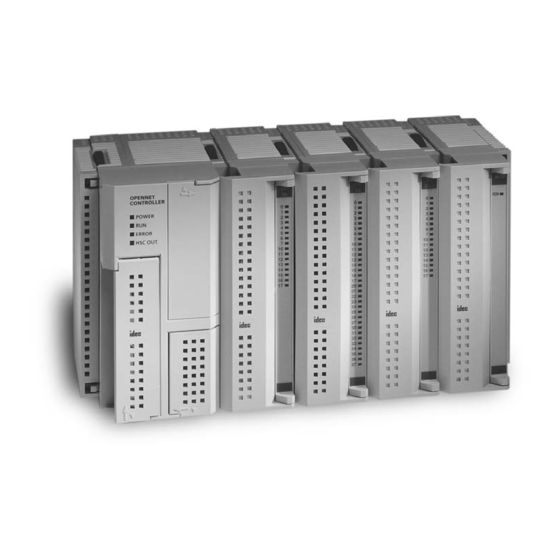
OpenNet interface modules and analog I/O modules can be mounted with one Open- CPU module. Net Controller ORKS DeviceNet RDY/ POWER FAIL ERROR HSC OUT SERVICE REQUEST idec idec idec Remote I/O Master Module Module OpenNet Interface Modules I/O Modules INTERBUS SX5S SX5S INTERBUS INTERBUS... - Page 13 CPU module has two RS232C ports and one RS485 port to control two RS232C devices and one OpenNet Controller RS485 device such as IDEC’s HG series operator interface at the same time. The figure below illustrates a system setup of remote I/O and user communication. In this example, the I/O statuses of a remote machine are transferred through the remote I/O line to the CPU.
- Page 14 1: G ENERAL NFORMATION Computer Link System When the is connected to a computer, operating status and I/O status can be monitored on the com- OpenNet Controller puter, data in the CPU module can be monitored or updated, and user programs can be downloaded and uploaded. A max- imum of 32 CPU modules can be connected to one computer in the 1:N computer link system.
- Page 15 1: G ENERAL NFORMATION Data Link System at the master station can communicate with 31 slave stations through the RS485 line to exchange OpenNet Controller data and perform distributed control effectively. The RS485 terminals are connected with each other using a 2-core twisted pair cable.
-
Page 16: Cpu Module
2: M ODULE PECIFICATIONS Introduction This chapter describes OpenNet Controller modules, parts names and specifications of each module. Available modules include CPU modules, digital I/O modules, analog I/O modules, expansion power supply module, remote I/O master module, and OpenNet interface modules such as DeviceNet slave and L interface modules. - Page 17 2: M ODULE PECIFICATIONS (1) Status LED POWER Turns on when power is supplied to the CPU Turns on when the CPU is running ERROR Turns on or flashes when an error occurs HSC OUT Turns on when the high-speed counter comparison output is on (2) Communication Enable Button Enables the communication mode selected with the communication selector DIP switch.
- Page 18 2: M ODULE PECIFICATIONS (8) Terminal Block Function Terminal No. Symbol Assignment High-speed counter COM High-speed counter phase A High-speed Counter High-speed counter phase B Terminals High-speed counter phase Z HSC OUT High-speed counter comparison output RS485 A RS485 line A RS485 Port RS485 B RS485 line B...
- Page 19 2: M ODULE PECIFICATIONS General Specifications Normal Operating Conditions Operating Temperature 0 to 55°C (operating ambient temperature) Storage Temperature –25 to +70°C Relative Humidity Level RH1, 30 to 95% (non-condensing) Pollution Degree 2 (IEC 60664-1) Corrosion Immunity Free from corrosive gases Operation: 0 to 2,000m (0 to 6,565 feet) Altitude Transport: 0 to 3,000m (0 to 9,840 feet)
- Page 20 2: M ODULE PECIFICATIONS Function Specifications CPU Module Specifications Program Capacity 16K words (8K steps) 7 slots maximum (without using expansion power supply module) Quantity of Slots 15 slots maximum (when using expansion power supply module) 224 points (without using expansion power supply module) 480 points (when using expansion power supply module) Maximum Digital •...
- Page 21 2: M ODULE PECIFICATIONS System Statuses at Stop, Reset, and Restart Internal Relays, Shift Registers, Timer Link Register Counters, Data Registers Mode Outputs Current Value (Note) Keep Type Clear Type Operating Operating Operating Operating Operating Reset (Reset input ON) OFF/Reset to zero OFF/Reset to zero Reset to zero Reset to zero...
-
Page 22: Input Module
2: M ODULE PECIFICATIONS Input Module Digital input modules are available in 16- and 32-point DC input modules and 8-point AC input modules. Four different connector/terminal styles are available. Input Module Type Numbers Module Name 16-point DC Input 32-point DC Input 8-point AC Input Screw Terminal FC3A-N16B1... - Page 23 2: M ODULE PECIFICATIONS 16-point DC Input Module Specifications Type No. FC3A-N16B1 FC3A-N16B3 Rated Input Voltage 24V DC sink/source input signal Input Voltage Range 19 to 30V DC Rated Input Current 7 mA/point (24V DC) Terminal Arrangement See Terminal Arrangement charts on pages 2-11 and 2-12. Input Impedance 3.4 kΩ...
- Page 24 2: M ODULE PECIFICATIONS 32-point DC Input Module Specifications Type No. FC3A-N32B4 FC3A-N32B5 Rated Input Voltage 24V DC sink/source input signal Input Voltage Range 20.4 to 27.6V DC Rated Input Current 4.9 mA/point (24V DC) Terminal Arrangement See Terminal Arrangement charts on pages 2-13 and 2-14. Input Impedance 4.7 kΩ...
- Page 25 2: M ODULE PECIFICATIONS 8-point AC Input Module Specifications Type No. FC3A-N08A11 Rated Input Voltage 100 to 120V AC Input Voltage Range 85 to 132V AC Rated Input Current 8.3 mA/point (100V AC, 60 Hz) Terminal Arrangement See Terminal Arrangement chart on page 2-15. Input Impedance 12 kΩ...
- Page 26 2: M ODULE PECIFICATIONS Input Module Terminal Arrangement FC3A-N16B1 (16-point DC Input Module) — Screw Terminal Type Applicable Connector: SMSTB2.5/20-ST-5.08 (Phoenix Contact) Terminal No. Name Wiring Schematic • COM terminals are connected together internally. • Terminal numbers are marked on the terminal block label on the input module. •...
- Page 27 2: M ODULE PECIFICATIONS FC3A-N16B3 (16-point DC Input Module) — Nylon Connector Type Applicable Connectors: VHR-10N (J.S.T. Mfg.) SVH-21T-P1.1 (J.S.T. Mfg.) Terminal No. Name Terminal No. Name Wiring Schematic • COM terminals are connected together internally. • Terminal numbers are marked on the female connector on the cable. •...
- Page 28 2: M ODULE PECIFICATIONS FC3A-N32B4 (32-point DC Input Module) — Nylon Connector Type Applicable Connector: H18-SHF-AA (J.S.T. Mfg.) SHF-001T-0.8BS (J.S.T. Mfg.) Terminal No. Name Terminal No. Name Wiring Schematic • COM terminals are connected together internally. • Terminal numbers are marked on the female connector on the cable. •...
- Page 29 2: M ODULE PECIFICATIONS FC3A-N32B5 (32-point DC Input Module) — Fujitsu Connector Type Applicable Connector: FCN-367J040-AU (Fujitsu) Terminal No. Name Terminal No. Name Wiring Schematic • COM terminals are connected together internally. • Terminal numbers are the front view of the male connector on the input module. •...
- Page 30 2: M ODULE PECIFICATIONS FC3A-N08A11 (8-point AC Input Module) — Screw Terminal Type Applicable Connector: SMSTB2.5/20-ST-5.08 (Phoenix Contact) Terminal No. Name COM0 COM1 COM2 COM3 COM4 COM5 COM6 COM7 Wiring Schematic • COM terminals are not connected together internally. • Terminal numbers are marked on the terminal block label on the input module. •...
-
Page 31: Output Module
2: M ODULE PECIFICATIONS Output Module Digital output modules are available in 16-point relay output modules, 16- and 32-point transistor sink output modules, and 16-point transistor protect source output modules. Five different connector/terminal styles are available. Output Module Type Numbers 16-point 16-point Transistor 16-point Transistor... - Page 32 2: M ODULE PECIFICATIONS 16-point Relay Output Module Specifications Type No. FC3A-R161 FC3A-R162 Terminal Arrangement See Terminal Arrangement charts on pages 2-22 and 2-23. Output Points and Common Lines 16 NO contacts in 4 common lines (COM terminals not connected together) 2A per point Maximum Load Current 8A per common line...
- Page 33 2: M ODULE PECIFICATIONS 16-point Transistor Sink Output Module Specifications Type No. FC3A-T16K1 FC3A-T16K3 Terminal Arrangement See Terminal Arrangement charts on pages 2-24 and 2-25. Rated Load Voltage 24V DC Operating Load Voltage Range 19 to 30V DC Rated Load Current 0.5A per output point 0.625A per output point (at 30V DC) Maximum Load Current...
- Page 34 2: M ODULE PECIFICATIONS 16-point Transistor Protect Source Output Module Specifications Type No. FC3A-T16P1 Terminal Arrangement See Terminal Arrangement chart on page 2-24. Rated Load Voltage 24V DC Operating Load Voltage Range 19 to 30V DC Rated Load Current 0.5A per output point 0.625A per output point (at 30V DC) Maximum Load Current 5A per common line (at 30V DC)
- Page 35 2: M ODULE PECIFICATIONS Special Data Registers D8030 through D8036 (Protect Transistor Output Error) • A prolonged overload or short circuit may damage the output circuit elements of the transistor Caution protect source output module. Include a protection program in the user program to protect the output module from damage caused by overheating.
- Page 36 2: M ODULE PECIFICATIONS 32-point Transistor Sink Output Module Specifications Type No. FC3A-T32K4 FC3A-T32K5 Terminal Arrangement See Terminal Arrangement charts on pages 2-26 and 2-27. Rated Load Voltage 24V DC Operating Load Voltage Range 20.4 to 27.6V DC Rated Load Current 0.1A per output point Maximum Load Current 0.115A per output point (at 27.6V DC)
- Page 37 2: M ODULE PECIFICATIONS Output Module Terminal Arrangement FC3A-R161 (16-point Relay Output Module) — Screw Terminal Type Applicable Connector: SMSTB2.5/20-ST-5.08 (Phoenix Contact) Terminal No. Name COM0 COM1 COM2 COM3 Wiring Schematic • COM terminals are not connected together internally. • Terminal numbers are marked on the terminal block label on the output module. •...
- Page 38 2: M ODULE PECIFICATIONS FC3A-R162 (16-point Relay Output Module) — Nylon Connector Type Applicable Connectors: VHR-5N (J.S.T. Mfg.) SVH-21T-P1.1 (J.S.T. Mfg.) Terminal No. Name Terminal No. Name COM0 COM2 Terminal No. Name Terminal No. Name COM1 COM3 Wiring Schematic • COM terminals are not connected together internally. •...
- Page 39 2: M ODULE PECIFICATIONS FC3A-T16K1/FC3A-T16P1 (16-point Transistor Sink and Protect Source Output Modules) — Screw Terminal Type Applicable Connector: SMSTB2.5/20-ST-5.08 (Phoenix Contact) FC3A-T16K1 FC3A-T16P1 Terminal No. Name Terminal No. Name COM(–) COM(+) –V COM(–) COM(+) –V Wiring Schematic • COM terminals are connected together internally. •...
- Page 40 2: M ODULE PECIFICATIONS FC3A-T16K3 (16-point Transistor Sink Output Module) — Nylon Connector Type Applicable Connector: VHR-10N (J.S.T. Mfg.) SVH-21T-P1.1 (J.S.T. Mfg.) Terminal No. Name COM(–) Terminal No. Name COM(–) Wiring Schematic • COM terminals are connected together internally. • Terminal numbers are marked on the female connector on the cable. •...
- Page 41 2: M ODULE PECIFICATIONS FC3A-T32K4 (32-point Transistor Sink Output Module) — Nylon Connector Type Applicable Connector: H18-SHF-AA (J.S.T. Mfg.) SHF-001T-0.8BS (J.S.T. Mfg.) Terminal No. Name Terminal No. Name COM(–) COM(–) Wiring Schematic • COM terminals are connected together internally. • Terminal numbers are marked on the female connector on the cable. •...
- Page 42 2: M ODULE PECIFICATIONS FC3A-T32K5 (32-point Transistor Sink Output Module) — Fujitsu Connector Type Applicable Connector: FCN-367J040-AU (Fujitsu) Terminal No. Name Terminal No. Name COM(–) COM(–) Wiring Schematic • COM terminals are connected together internally. • Terminal numbers are the front view of the male connector on the output module. •...
-
Page 43: Analog Input Module (A/D Converter)
2: M ODULE PECIFICATIONS Analog Input Module (A/D Converter) The 12-bit analog input module converts 6 channels of analog signals to digital data of 0 through 4000 which can be pro- cessed using advanced instructions such as the coordinate conversion instruction. The analog input module is a functional module and the converted digital data is stored to a link register, depending on the analog channel and the mounting slot number of the analog input module in the system setup. - Page 44 2: M ODULE PECIFICATIONS Analog Input Module Specifications Type No. FC3A-AD1261 Quantity of Input Channels 6 channels Terminal Arrangement See page 2-30. Voltage input: 1 MΩ minimum Input Impedance within Signal Range Current input: 250Ω Maximum Error at 25°C ±0.6% of full scale Temperature Coefficient ±0.013 %/°C (typical) Input Error...
- Page 45 2: M ODULE PECIFICATIONS Analog Input Module Terminal Arrangement FC3A-AD1261 (6-channel Analog Input Module) — Screw Terminal Type Applicable Connector: SMSTB2.5/20-ST-5.08 (Phoenix Contact) Terminal No. Channel Name +V (voltage) Channel 0 +I (current) COM (–V, –I) +V (voltage) Channel 1 +I (current) COM (–V, –I) +V (voltage)
-
Page 46: Analog Output Module (D/A Converter)
2: M ODULE PECIFICATIONS Analog Output Module (D/A Converter) The 12-bit analog output module converts digital data of 0 through 4000 to 2 channels of analog signals. The analog output module is a functional module and the digital data for conversion must be stored to a link register, depending on the analog channel and the mounting slot number of the analog output module in the system setup. - Page 47 2: M ODULE PECIFICATIONS Analog Output Module Specifications Type No. FC3A-DA1221 Quantity of Output Channels 2 channels Terminal Arrangement See page 2-33. Maximum Error at 25°C ±0.6% of full scale Temperature Coefficient ±0.013 %/°C (typical) Output Error Maximum Error over Full ±1% of full scale Temperature Range Digital Resolution...
- Page 48 2: M ODULE PECIFICATIONS Analog Output Module Terminal Arrangement FC3A-DA1221 (2-channel Analog Output Module) — Screw Terminal Type Applicable Connector: SMSTB2.5/20-ST-5.08 (Phoenix Contact) Rotary Switch Terminal No. Channel Name Position Voltage output (0 to 10V) COM (GND) Voltage output (±10V) COM (GND) Voltage output (0 to 5V) Channel 0...
-
Page 49: Expansion Power Supply Module
2: M ODULE PECIFICATIONS Expansion Power Supply Module The FC3A-EA1 expansion power supply module is used to mount more than seven I/O and functional modules. When a maximum of 15 I/O modules are mounted, the number of I/O points is expanded from 224 to 480 maximum. Whether an expansion module is used or not, seven functional modules such as analog I/O, DeviceNet slave, and L interface modules can be mounted at the maximum in either the normal or expansion slots. - Page 50 2: M ODULE PECIFICATIONS Expansion Power Supply Module Specifications Type No. FC3A-EA1 Rated Power Voltage 24V DC Allowable Voltage Range 19 to 30V DC (including ripple) Dielectric Strength Between power terminal and FG: 1,000V AC, 1 minute Maximum Input Current 5A at 24V DC Internal Current Draw 30 mA (24V DC)
-
Page 51: Remote I/O Master Module
OpenNet Controller For the remote I/O slave stations, IDEC’s SX5S communication I/O terminals are used. When using 32 SX5S modules with 16 input or output points, a total of 512 I/O points can be distributed to 32 remote slave stations at the maximum. - Page 52 2: M ODULE PECIFICATIONS Remote I/O Master Module General Specifications Type No. FC3A-SX5SM1 Power Voltage Supplied by the CPU module Dielectric Strength Between power terminal on the CPU module and FG: 500V AC, 1 minute Between REMOTE OUT terminal and FG: 10 MΩ minimum (500V DC megger) Insulation Resistance Between V.24 Interface terminal and FG: 10 MΩ...
-
Page 53: Devicenet Slave Module
2: M ODULE PECIFICATIONS DeviceNet Slave Module can be linked to DeviceNet networks. For communication through the DeviceNet network, the OpenNet Controller DeviceNet slave module is available. For details about the DeviceNet slave module and DeviceNet communication system, see page 25-1. DeviceNet Slave Module Type Number and Weight Module Name DeviceNet Slave Module... - Page 54 2: M ODULE PECIFICATIONS Interface Module ORKS can be linked to L networks. For communication through the L network, the OpenNet Controller ORKS ORKS interface module is available. ORKS For details about the L interface module and L communication system, see page 26-1. ORKS ORKS Interface Module Type Number and Weight...
-
Page 55: Dimensions
L interface modules have the same outside dimensions. ORKS Example: The following figure illustrates a system setup consisting of a remote I/O master module, a CPU module, and three I/O modules. idec All dimensions in mm. 2-40 ’ ONTROLLER ANUAL Phone: 800.894.0412 - Fax: 888.723.4773 - Web: www.clrwtr.com - Email: info@clrwtr.com... -
Page 56: Installation Location
3: I NSTALLATION AND IRING Introduction This chapter describes the methods and precautions for installing and wiring OpenNet Controller modules. Before starting installation and wiring, be sure to read “Safety Precautions” in the beginning of this manual and under- stand precautions described under Warning and Caution. •... -
Page 57: Assembling Modules
3: I NSTALLATION AND IRING Assembling Modules • Assemble modules together before mounting the modules onto a DIN rail. OpenNet Controller Caution Attempt to assemble modules on a DIN rail may cause damage to the modules. • When using analog input or output modules, first set the rotary switch on the side of the module to the desired input/output mode before assembling the module. -
Page 58: Disassembling Modules
OpenNet Controller • Mount the OpenNet Controller modules on a 35-mm-wide DIN rail. Applicable DIN rail: IDEC’s BAA1000 (1000mm/39.4” long) 1. Fasten the DIN rail to a panel using screws firmly. 2. Pull out the clamp from each module, and put OpenNet Controller the groove of the module on the DIN rail. -
Page 59: Installation In Control Panel
3: I NSTALLATION AND IRING Installation in Control Panel modules are designed for installation in equipment. Do not install the mod- OpenNet Controller OpenNet Controller ules outside equipment. The environment for using the OpenNet Controller is “Pollution degree 2.” Use the OpenNet Controller in environments of pollution degree 2 (according to IEC 60664-1). -
Page 60: Input Wiring
3: I NSTALLATION AND IRING Input Wiring • Terminal name “NC” means “No Connection.” Do not connect input or any other wiring to NC Caution terminals. • Separate the input wiring from the output line, power line, and motor line. •... -
Page 61: Output Wiring
3: I NSTALLATION AND IRING Output Wiring Caution • Terminal name “NC” means “No Connection.” Do not connect output or any other wiring to NC terminals. • If relays or transistors in the OpenNet Controller output modules should fail, outputs may remain on or off. For output signals which may cause heavy accidents, provide a monitor circuit outside the OpenNet Controller •... -
Page 62: Data Link Wiring
3: I NSTALLATION AND IRING Output Wiring for Application in Europe When equipment containing the is intended for use in European countries, insert an IEC 60127- OpenNet Controller approved fuse to each output of every output module for protection against overload or short-circuit. This is required when exporting equipment containing the to Europe. -
Page 63: Analog Input/Output Wiring
3: I NSTALLATION AND IRING Analog Input/Output Wiring When using an analog input or output module, connect analog signals and ground wire as shown below. • For wiring analog input or output module, use a two-core twisted pair shielded cable with a minimum core diameter of 0.9 mm. -
Page 64: Power Supply
3: I NSTALLATION AND IRING Power Supply • Use a power supply of the rated value. Use of a wrong power supply may cause fire hazard. Caution • The allowable power voltage range for the is 19 to 30V DC. Do not use the OpenNet Controller on any other voltage. -
Page 65: Terminal Connection
3: I NSTALLATION AND IRING Terminal Connection • Make sure that the operating conditions and environments are within the specification values. Caution • Be sure to connect the grounding wire to a proper ground, otherwise electrical shocks may be caused. •... -
Page 66: Connecting Opennet Controller To Pc (1:1 Computer Link System)
4: O PERATION ASICS Introduction This chapter describes general information about setting up the basic OpenNet Controller system for programming, start- ing and stopping OpenNet Controller operation, and introduces simple operating procedures from creating a user program using WindLDR on a computer to monitoring the OpenNet Controller operation. -
Page 67: Start/Stop Operation
4: O PERATION ASICS Start/Stop Operation This section describes operations to start and stop the and to use the stop and reset inputs. OpenNet Controller • Make sure of safety before starting and stopping the . Incorrect operation on OpenNet Controller Caution may cause machine damage or accidents. - Page 68 4: O PERATION ASICS Start/Stop Operation Using the Power Supply can be started and stopped by turning power on and off. OpenNet Controller 1. Power up the to start operation. See page 4-1. OpenNet Controller 2. If the OpenNet Controller does not start, check that start control special internal relay M8000 is on using WindLDR .
-
Page 69: Simple Operation
4: O PERATION ASICS Simple Operation This section describes how to edit a simple program using on a computer, transfer the program from WindLDR WindLDR the PC to the , run the program, and monitor the operation on OpenNet Controller WindLDR Connect the OpenNet Controller... - Page 70 4: O PERATION ASICS 2. Move the mouse pointer to the first column of the first line where you want to insert a NO contact, and click the left mouse button. The Normally Open dialog box appears. 3. Enter I0 in the Tag Name field, and click OK. A NO contact of input I0 is programmed in the first column of the first ladder line.
- Page 71 4: O PERATION ASICS A new rung is inserted by pressing the Enter key while the cursor is on the preceding rung. A new rung can also be inserted by selecting Edit > Append > Rung. When completed, the ladder program looks like below. Now, save the file with a new name.
- Page 72 4: O PERATION ASICS Monitor Operation Another powerful function of is to monitor the PLC operation on the PC. The input and output statuses of the WindLDR sample program can be monitored in the ladder diagram. From the WindLDR menu bar, select Online > Monitor. When both inputs I0 and I1 are on, the ladder diagram on the monitor screen looks as follows: Rung 01: When both inputs I0 and I1 are on, output Q0 is turned off.
- Page 73 4: O PERATION ASICS ’ ONTROLLER ANUAL Phone: 800.894.0412 - Fax: 888.723.4773 - Web: www.clrwtr.com - Email: info@clrwtr.com...
-
Page 74: Stop Input And Reset Input
5: S PECIAL UNCTIONS Introduction OpenNet Controller features special functions such as stop/reset inputs, run/stop selection at memory backup error, keep designation for internal relays, shift registers, counters, and data registers. These functions are programmed using the Function Area Settings menu. Also included in the Function Area Settings are module ID selection and run/stop operation upon disparity, input filter, catch input, high-speed counter, key matrix input, and user program read/write protection. -
Page 75: Run/Stop Selection At Memory Backup Error
5: S PECIAL UNCTIONS Run/Stop Selection at Memory Backup Error Start control special internal relay M8000 maintains its status when the CPU is powered down. After the CPU has been off for a period longer than the battery backup duration, the data designated to be maintained during power failure is broken. The Run/Stop Selection at Memory Backup Error dialog box is used to select whether to start or stop the CPU when attempting to restart operation after the “keep”... -
Page 76: Keep Designation For Internal Relays, Shift Registers, Counters, And Data Registers
5: S PECIAL UNCTIONS Keep Designation for Internal Relays, Shift Registers, Counters, and Data Registers The statuses of internal relays and shift register bits are usually cleared at startup. It is also possible to designate all or a block of consecutive internal relays or shift register bits as “keep” types. Counter current values and data register values are usually maintained at powerup. - Page 77 5: S PECIAL UNCTIONS Internal Relay ‘Keep’ Designation All Clear: All internal relay statuses are cleared at startup (default). All Keep: All internal relay statuses are maintained at startup. Keep Range: A designated area of internal relays are maintained at startup. Enter the start “keep” number in the left field and the end “keep”...
-
Page 78: Module Id Selection And Run/Stop Operation Upon Disparity
5: S PECIAL UNCTIONS Module ID Selection and Run/Stop Operation upon Disparity The CPU module can be mounted with a maximum of seven I/O modules and functional modules without using an expan- sion power supply module. When using an expansion power supply module, a maximum of 15 modules can be mounted with one CPU module. -
Page 79: Input Filter
5: S PECIAL UNCTIONS Input Filter The input filter function is used to reject input noises. The catch input function described in the next section is used to receive short input pulses. On the contrary, the input filter function ignores short input pulses when the OpenNet Controller is used with input signals containing noises. -
Page 80: Catch Input
5: S PECIAL UNCTIONS Catch Input The catch input function is used to receive short pulses from sensor outputs regardless of the scan time. Input pulses shorter than one scan time can be received. First eight inputs of every DC input module can be designated to catch a rising or falling edge of short input pulses. - Page 81 5: S PECIAL UNCTIONS Catching Rising Edge of Input Pulse Note 1 Actual Input Note 2 Input Relay (I0 to I7) One Scan Processed Catching Falling Edge of Input Pulse Note 1 Actual Input Note 2 Input Relay (I0 to I7) Processed Note 1: When two or more pulses enter within one scan, subsequent pulses are ignored.
-
Page 82: High-Speed Counter
5: S PECIAL UNCTIONS High-speed Counter This section describes the high-speed counter function to count many pulse inputs within one scan. Using the built-in 16- bit high-speed counter, the counts up to 65535 high-speed pulses from a rotary encoder or proximity OpenNet Controller switch without regard to the scan time, compares the current value with a preset value, and turns on the output when the current value exceeds the preset value. - Page 83 5: S PECIAL UNCTIONS High-speed Counter Input Specifications Maximum Counting Frequency 10 kHz Counting Range 0 to 65535 (16 bits) Input Voltage 24V DC ±15% Input Impedance 6 kΩ High-speed Counter Output Specifications Comparison Output 1 point (terminal 5 on the CPU module) Output Device Transistor sink or source output depending on the CPU module type Output Power Voltage...
- Page 84 5: S PECIAL UNCTIONS Programming WindLDR 1. From the menu bar, select Configure > Function Area Settings. The Function Area Setting dialog box WindLDR appears. 2. Select the Others tab. 3. Click the Enable High-speed Counter check box. HSC Operation Mode Two operation modes are available.
- Page 85 5: S PECIAL UNCTIONS High-speed Counter Timing Chart Current Value The D8047 value at this point becomes the preset value for the next counting cycle. 65535 65534 Preset Value one scan one scan one scan one scan Phase Z Input (Terminal 4) Comparison Output (Terminal 5) Comparison Output Reset M8010 Up/Down Status M8130...
- Page 86 5: S PECIAL UNCTIONS High-speed Counter Wiring Diagram Sink Type High-speed Counter Comparison Output — FC3A-CP2K and FC3A-CP2KM Wiring for loads insusceptible to noises Wiring for loads susceptible to noises Reset to zero Reset to zero HSC OUT HSC OUT +24V DC +24V DC Source Type High-speed Counter Comparison Output —...
- Page 87 5: S PECIAL UNCTIONS Example: Counting High-speed Input Pulses from Rotary Encoder This example demonstrates a program to punch holes in a paper tape at regular intervals. Description of Operation A rotary encoder is linked to the tape feed roller directly, and Rolled Tape the output pulses from the rotary encoder are counted by the high-speed counter in the...
- Page 88 5: S PECIAL UNCTIONS Programming WindLDR Timing Chart When the high-speed counter current value reaches 3000, the comparison output is turned on and the current value is reset to 300. Current Value Preset Value D8047 2999 Reset Value D8046 Comparison Output Status M8135 0.5 sec for punching Comparison Comparison output status M8135 turns on in...
-
Page 89: Key Matrix Input
5: S PECIAL UNCTIONS Key Matrix Input The key matrix input function can be programmed using the Function Area Settings in to form a matrix with 1 to WindLDR 16 input points and 1 to 16 output points to multiply input capability. A key matrix with 8 inputs and 4 outputs would equal 32 inputs, for example. - Page 90 5: S PECIAL UNCTIONS Key Matrix Circuit The key matrix structure includes sequentially-numbered input points along the top and sequentially-numbered output points along the side. The I/O connecting blocks include a diode and a switch, as shown below. DC Input Module Input SW00 SW01...
-
Page 91: User Program Protection
5: S PECIAL UNCTIONS User Program Protection The user program in the CPU module can be protected from reading, writing, or both using the Func- OpenNet Controller tion Area Settings in WindLDR • When proceeding with the following steps, make sure to note the protect code, which is needed to Warning disable the user program protection. -
Page 92: Memory Card
5: S PECIAL UNCTIONS Memory Card A user program can be stored on a miniature memory card from a computer running and downloaded to the WindLDR CPU module without using a computer. This feature is available on FC3A-CP2KM and FC3A- OpenNet Controller CP2SM only. -
Page 93: Constant Scan Time
5: S PECIAL UNCTIONS Constant Scan Time The scan time may vary whether basic and advanced instructions are executed or not depending on input conditions to these instructions. The scan time can be made constant by entering a required scan time preset value into special data reg- ister D8022 reserved for constant scan time. - Page 94 6: A LLOCATION UMBERS Introduction This chapter describes allocation numbers available for the OpenNet Controller CPU module to program basic and advanced instructions. Special internal relays and special data registers are also described. OpenNet Controller is programmed using operands such as inputs, outputs, internal relays, timers, counters, shift reg- isters, data registers, and link registers.
-
Page 95: Operand Allocation Numbers
6: A LLOCATION UMBERS Operand Allocation Numbers Operand Allocation Numbers Total Points I0000-I0007 I0010-I0017 I0020-I0027 I0030-I0037 I0040-I0047 I0050-I0057 I0060-I0067 I0070-I0077 I0080-I0087 I0090-I0097 I0100-I0107 I0110-I0117 I0120-I0127 I0130-I0137 I0140-I0147 I0150-I0157 I0160-I0167 I0170-I0177 I0180-I0187 I0190-I0197 I0200-I0207 I0210-I0217 I0220-I0227 I0230-I0237 I0240-I0247 I0250-I0257 I0260-I0267 I0270-I0277 Input (I) I0280-I0287 I0290-I0297 I0300-I0307 I0310-I0317 I0320-I0327 I0330-I0337 I0340-I0347 I0350-I0357... - Page 96 6: A LLOCATION UMBERS Operand Allocation Numbers Total Points M1000-M1007 M1010-M1017 M1020-M1027 M1030-M1037 M1040-M1047 M1050-M1057 M1060-M1067 M1070-M1077 M1080-M1087 M1090-M1097 M1100-M1107 M1110-M1117 M1120-M1127 M1130-M1137 M1140-M1147 M1150-M1157 M1160-M1167 M1170-M1177 M1180-M1187 M1190-M1197 M1200-M1207 M1210-M1217 M1220-M1227 M1230-M1237 M1240-M1247 M1250-M1257 M1260-M1267 M1270-M1277 M1280-M1287 M1290-M1297 M1300-M1307 M1310-M1317 M1320-M1327 M1330-M1337 M1340-M1347 M1350-M1357 M1360-M1367 M1370-M1377 M1380-M1387 M1390-M1397 M1400-M1407 M1410-M1417 M1420-M1427 M1430-M1437...
-
Page 97: Operand Allocation Numbers For Functional Modules
6: A LLOCATION UMBERS Operand Allocation Numbers for Functional Modules Allocation Numbers Functional Module Status Area Reserved Area Data Area (Read Only) (Access Prohibited) Functional Module 1 L0100-L0107 L0110-L0117 L0120-L0127 Functional Module 2 L0200-L0207 L0210-L0217 L0220-L0227 Functional Module 3 L0300-L0307 L0310-L0317 L0320-L0327 Functional Module 4... -
Page 98: Operand Allocation Numbers For Data Link Master Station
6: A LLOCATION UMBERS Operand Allocation Numbers for Data Link Master Station Allocation Number Slave Station Number Transmit Data Receive Data Data Link to Slave Station from Slave Station Communication Error Slave Station 1 D7000-D7009 D7010-D7019 D8400 Slave Station 2 D7020-D7029 D7030-D7039 D8401... -
Page 99: Special Internal Relay Allocation Numbers
6: A LLOCATION UMBERS Special Internal Relay Allocation Numbers Special internal relays M8000 through M8117 are read/write internal relays used for controlling the CPU operation and communication. Special internal relays M8120 through M8237 are read-only internal relays primarily used for indicating the CPU statuses. - Page 100 6: A LLOCATION UMBERS Allocation Description CPU Stopped Power OFF Number M8065 RS232C Port 1 Modem Mode (Answer): Initialization String Completion Maintained Cleared M8066 RS232C Port 1 Modem Mode (Answer): ATZ Completion Maintained Cleared M8067 RS232C Port 1 Modem Mode Operational State Maintained Cleared M8070...
- Page 101 6: A LLOCATION UMBERS Allocation Description CPU Stopped Power OFF Number M8125 In-operation Output Cleared Cleared M8126-M8127 — Reserved — — — M8130 High-speed Counter Up/Down Status Maintained Cleared M8131 High-speed Counter Comparison ON Status (ON for 1 scan) Maintained Cleared M8132 High-speed Counter Current Value Zero-clear (ON for 1 scan)
- Page 102 6: A LLOCATION UMBERS M8000 Start Control M8000 indicates the operating status of the OpenNet Controller . The OpenNet Controller stops operation when M8000 is turned off while the CPU is running. M8000 can be turned on or off using the WindLDR Online menu.
- Page 103 flag of a user communication RXD instruction is turned on, without wait- ing for the END processing. M8014 is valid for all communication ports; RS232C port 1 and port 2, and RS485. When an IDEC’s HG series operator interface is linked to the OpenNet Controller...
- Page 104 6: A LLOCATION UMBERS M8122 100-msec Clock 50 msec 50 msec M8122 always generates clock pulses in 100-msec increments, whether M8001 is on or off, with a duty ratio of 1:1 (50 msec on M8122 and 50 msec off). 100 msec M8123 10-msec Clock 5 msec 5 msec...
-
Page 105: Special Data Registers
6: A LLOCATION UMBERS Special Data Registers Special Data Register Allocation Numbers Allocation Description Updated See Page Number D8000 System Setup ID (Quantity of Inputs) When I/O initialized D8001 System Setup ID (Quantity of Outputs) When I/O initialized D8002 System Setup ID (Quantity of Functional Modules) When I/O initialized D8003 System Setup ID (Data Link Usage) —... - Page 106 6: A LLOCATION UMBERS Special Data Registers for High-speed Counter Allocation Description Updated See Page Number D8045 High-speed Counter Current Value Every scan 5-10 D8046 High-speed Counter Reset Value 5-10 D8047 High-speed Counter Preset Value 5-10 D8048-D8049 — Reserved — —...
- Page 107 6: A LLOCATION UMBERS Allocation Description Updated See Page Number D8084 INTERBUS (Node 8) ID Code When initialized 24-6 D8085 INTERBUS (Node 8) Device Level When initialized 24-6 D8086 INTERBUS (Node 9) Logical Device No. When initialized 24-6 D8087 INTERBUS (Node 9) Length Code When initialized 24-6 D8088...
- Page 108 6: A LLOCATION UMBERS Allocation Description Updated See Page Number D8128 INTERBUS (Node 19) ID Code When initialized 24-6 D8129 INTERBUS (Node 19) Device Level When initialized 24-6 D8130 INTERBUS (Node 20) Logical Device No. When initialized 24-6 D8131 INTERBUS (Node 20) Length Code When initialized 24-6 D8132...
- Page 109 6: A LLOCATION UMBERS Allocation Description Updated See Page Number D8172 INTERBUS (Node 30) ID Code When initialized 24-6 D8173 INTERBUS (Node 30) Device Level When initialized 24-6 D8174 INTERBUS (Node 31) Logical Device No. When initialized 24-6 D8175 INTERBUS (Node 31) Length Code When initialized 24-6 D8176...
- Page 110 6: A LLOCATION UMBERS Allocation Description Updated See Page Number D8310 Port 2 Retry Interval Every scan during retry 23-3 D8311 Port 2 Modem Mode Status At status transition 23-3 D8312-D8314 — Reserved — — — D8315-D8329 Port 2 AT Command Result Code When returning result code 23-3 D8330-D8344...
-
Page 111: Digital I/O Module Operands
6: A LLOCATION UMBERS Digital I/O Module Operands Input and output numbers are automatically allocated to each digital I/O module in the order of increasing distance from the CPU module. A maximum of 7 digital I/O or functional modules can be mounted with one CPU module without using an expansion power supply module, so that a maximum of 224 I/O points can be allocated in total. -
Page 112: Bit Designation Of Link Register
6: A LLOCATION UMBERS Example: Slot No.: OpenNet Func- Output Func- Output Func- Input Controller tional Module tional Module tional Module CPU Module Module Module Module 32-pt 16-pt 32-pt Analog Analog OpenNet Output Output Input Output Input Interface The system setup shown above will have operand numbers allocated to each module as follows: Slot No. - Page 113 6: A LLOCATION UMBERS 6-20 ’ ONTROLLER ANUAL Phone: 800.894.0412 - Fax: 888.723.4773 - Web: www.clrwtr.com - Email: info@clrwtr.com...
-
Page 114: Basic Instruction List
7: B ASIC NSTRUCTIONS Introduction This chapter describes programming of the basic instructions, available operands, and sample programs. Basic Instruction List Symbol Name Function Words Series connection of NO contact AND LOD And Load Series connection of circuit blocks ANDN And Not Series connection of NC contact Restores the result of bit logical operation which was saved... -
Page 115: Lod (Load) And Lodn (Load Not)
7: B ASIC NSTRUCTIONS LOD (Load) and LODN (Load Not) The LOD instruction starts the logical operation with a NO (normally open) contact. The LODN instruction starts the log- ical operation with a NC (normally closed) contact. A total of eight LOD and/or LODN instructions can be programmed consecutively. Ladder Diagram Valid Operands Instruction... -
Page 116: Set And Rst (Reset)
7: B ASIC NSTRUCTIONS Examples: LOD (Load), NOT, and OUT (Output) Ladder Diagram Program List Timing Chart Prgm Adrs Instruction Data LODN OUTN Ladder Diagram Program List Prgm Adrs Instruction Data Ladder Diagram Program List Prgm Adrs Instruction Data LODN Ladder Diagram Program List Prgm Adrs... -
Page 117: And And Andn (And Not)
7: B ASIC NSTRUCTIONS and ANDN (And Not) The AND instruction is used for programming a NO contact in series. The ANDN instruction is used for programming a NC contact in series. The AND or ANDN instruction is entered after the first set of contacts. Ladder Diagram Program List Timing Chart... -
Page 118: And Lod (Load)
7: B ASIC NSTRUCTIONS AND LOD (Load) The AND LOD instruction is used to connect, in series, two or more circuits starting with the LOD instruction. The AND LOD instruction is the equivalent of a “node” on a ladder diagram. When using WindLDR , the user need not program the AND LOD instruction. -
Page 119: Bps (Bit Push), Brd (Bit Read), And Bpp (Bit Pop)
7: B ASIC NSTRUCTIONS BPS (Bit Push), BRD (Bit Read), and BPP (Bit Pop) The BPS (bit push) instruction is used to save the result of bit logical operation temporarily. The BRD (bit read) instruction is used to read the result of bit logical operation which was saved temporarily. The BPP (bit pop) instruction is used to restore the result of bit logical operation which was saved temporarily. - Page 120 7: B ASIC NSTRUCTIONS Data Movement in Operation Register and Bit Stack Register When the BPS (bit push) instruction is used, the program in the operation register is stored in the first bit stack register. When the BPS instruction is used again, the program in the first stack register is stored in the second bit stack register and the program in the operation register is stored in the first stack register.
-
Page 121: Tml, Tim, Tmh, And Tms (Timer)
7: B ASIC NSTRUCTIONS TML, TIM, TMH, and TMS (Timer) Four types of timers are available; 1-sec timedown timer TML, 100-msec timedown timer TIM, 10-msec timedown timer TMH, and 1-msec timedown timer TMS. A total of 256 timers can be programmed in a user program. Each timer must be allocated to a unique number T0 through T255. - Page 122 7: B ASIC NSTRUCTIONS Timer Circuit The preset value 0 through 65535 can be designated using a data register D0 through D7999; then the data of the data reg- ister becomes the preset value. Directly after the TML, TIM, TMH, or TMS instruction, the OUT, OUTN, SET, RST, TML, TIM, TMH, or TMS instruction can be programmed.
- Page 123 7: B ASIC NSTRUCTIONS Timer Accuracy, continued Timer Counting Error Every timer instruction operation is individually based on asynchronous 16-bit reference timers. Therefore, an error occurs depending on the status of the asynchronous 16-bit timer when the timer instruction is executed. Error (1-sec timer) (100-msec timer)
-
Page 124: Cnt, Cdp, And Cud (Counter)
7: B ASIC NSTRUCTIONS CNT, CDP, and CUD (Counter) Three types of counters are available; adding (up) counter CNT, dual-pulse reversible counter CDP, and up/down selection reversible counter CUD. A total of 256 counters can be programmed in a user program. Each counter must be allocated to a unique number C0 through C255. - Page 125 7: B ASIC NSTRUCTIONS CDP (Dual-Pulse Reversible Counter) The dual-pulse reversible counter CDP has up and down pulse inputs, so that three inputs are required. The circuit for a dual-pulse reversible counter must be programmed in the following order: preset input, up-pulse input, down-pulse input, the CDP instruction, and a counter number C0 through C255, followed by a counter preset value from 0 to 65535.
- Page 126 7: B ASIC NSTRUCTIONS CUD (Up/Down Selection Reversible Counter) The up/down selection reversible counter CUD has a selection input to switch the up/down gate, so that three inputs are required. The circuit for an up/down selection reversible counter must be programmed in the following order: preset input, pulse input, up/down selection input, the CUD instruction, and a counter number C0 through C255, followed by a counter preset value from 0 to 65535.
-
Page 127: Cc= And Cc≥ (Counter Comparison)
7: B ASIC NSTRUCTIONS CC= and CC≥ (Counter Comparison) The CC= instruction is an equivalent comparison instruction for counter current values. This instruction will constantly compare current values to the value that has been programmed in. When the counter value equals the given value, the desired output will be initiated. - Page 128 7: B ASIC NSTRUCTIONS Examples: CC= and CC≥ (Counter Comparison) Ladder Diagram 1 Program List Reset Prgm Adrs Instruction Data Rung 1 Pulse Rung 2 CC≥ CC>= Timing Chart Reset Input I0 Pulse Input I1 • • • Output Q0 is on when counter C2 current value is 5.
-
Page 129: Tc= And Tc≥ (Timer Comparison)
7: B ASIC NSTRUCTIONS TC= and TC≥ (Timer Comparison) The TC= instruction is an equivalent comparison instruction for timer current values. This instruction will constantly com- pare current values to the value that has been programmed in. When the timer value equals the given value, the desired out- put will be initiated. - Page 130 7: B ASIC NSTRUCTIONS Examples: TC= and TC≥ (Timer Comparison) Ladder Diagram 1 Program List Prgm Adrs Instruction Data TC>= TC≥ Timing Chart Input I0 Output Q0 is on when timer T2 current value 100 99 • • • 51 50 49 •...
-
Page 131: Dc= And Dc≥ (Data Register Comparison)
7: B ASIC NSTRUCTIONS DC= and DC≥ (Data Register Comparison) The DC= instruction is an equivalent comparison instruction for data register values. This instruction will constantly com- pare data register values to the value that has been programmed in. When the data register value equals the given value, the desired output will be initiated. - Page 132 7: B ASIC NSTRUCTIONS Examples: DC= and DC≥ (Data Register Comparison) Ladder Diagram 1 Program List Prgm Adrs Instruction Data MOV(W) S1 – D1 – MOV(W) D10 – – DC>= DC≥ Timing Chart Input I1 D10 Value 10 10 D2 Value Output Q0 is on when data register D2 value is 5.
-
Page 133: Sfr And Sfrn (Forward And Reverse Shift Register)
7: B ASIC NSTRUCTIONS SFR and SFRN (Forward and Reverse Shift Register) The shift register consists of a total of 256 bits which are allocated to R0 through R255. Any number of available bits can be selected to form a train of bits which store on or off status. The on/off data of constituent bits is shifted in the forward direction (forward shift register) or in the reverse direction (reverse shift register) when a pulse input is turned on. - Page 134 7: B ASIC NSTRUCTIONS Forward Shift Register (SFR), continued Ladder Diagram Program List Reset Prgm Adrs Instruction Data Rung 1 Rung 1 0 Pulse Data Rung 2 5 Rung 2 Timing Chart Reset Input I0 One scan or more is required Pulse Input I1 Data Input I2 R0/Q0...
- Page 135 7: B ASIC NSTRUCTIONS Reverse Shift Register (SFRN) For reverse shifting, use the SFRN instruction. When SFRN instructions are programmed, two addresses are always required. The SFRN instructions are entered, followed by a shift register number selected from appropriate operand num- bers.
- Page 136 7: B ASIC NSTRUCTIONS Bidirectional Shift Register A bidirectional shift register can be created by first programming the SFR instruction as detailed in the Forward Shift Reg- ister section on page 7-20. Next, the SFRN instruction is programed as detailed in the Reverse Shift Register section on page 7-22.
-
Page 137: Sotu And Sotd (Single Output Up And Down)
7: B ASIC NSTRUCTIONS SOTU and SOTD (Single Output Up and Down) The SOTU instruction “looks for” the transition of a given input from off to on. The SOTD instruction looks for the transi- tion of a given input from on to off. When this transition occurs, the desired output will turn on for the length of one scan. The SOTU or SOTD instruction converts an input signal to a “one-shot”... -
Page 138: Mcs And Mcr (Master Control Set And Reset)
7: B ASIC NSTRUCTIONS and MCR (Master Control Set and Reset) The MCS (master control set) instruction is usually used in combination with the MCR (master control reset) instruction. The MCS instruction can also be used with the END instruction, instead of the MCR instruction. When the input preceding the MCS instruction is off, the MCS is executed so that all inputs to the portion between the MCS and the MCR are forced off. - Page 139 7: B ASIC NSTRUCTIONS MCS and MCR (Master Control Set and Reset), continued Multiple Usage of MCS instructions Ladder Diagram Program List Prgm Adrs Instruction Data This master control circuit will give priority to I1, I3, and I5, in that order. When input I1 is off, the first MCS is executed so that subsequent inputs I2 through I6 are forced off.
-
Page 140: Jmp (Jump) And Jend (Jump End)
7: B ASIC NSTRUCTIONS JMP (Jump) and JEND (Jump End) The JMP (jump) instruction is usually used in combination with the JEND (jump end) instruction. At the end of a program, the JMP instruction can also be used with the END instruction, instead of the JEND instruction. These instructions are used to proceed through the portion of the program between the JMP and the JEND without pro- cessing. -
Page 141: Jmp (Jump) And Jend (Jump End)
7: B ASIC NSTRUCTIONS JMP (Jump) and JEND (Jump End), continued Ladder Diagram Program List Prgm Adrs Instruction Data JEND JEND This jump circuit will give priority to I1, I3, and I5, in that order. When input I1 is on, the first JMP is executed so that subsequent output statuses of Q0 through Q2 are held. When input I1 is off, the first JMP is not executed so that the following program is executed according to the actual input statuses of I2 through I6. -
Page 142: Advanced Instruction List
8: A DVANCED NSTRUCTIONS Introduction This chapter describes general rules of using advanced instructions, terms, data types, and formats used for advanced instructions. Advanced Instruction List Data Type Qty of Group Symbol Name Words Page No Operation Move 6 or 7 MOVN Move Not 6 or 7... - Page 143 8: A DVANCED NSTRUCTIONS Data Type Qty of Group Symbol Name Words Page SFTL Shift Left 13-1 SFTR Shift Right 13-3 ROTL Rotate Left 13-5 Bit Shift ROTR Rotate Right 13-7 Rotate ROTLC Rotate Left with Carry 13-9 ROTRC Rotate Right with Carry 13-11 BCDLS BCD Left Shift...
-
Page 144: Structure Of An Advanced Instruction
8: A DVANCED NSTRUCTIONS Structure of an Advanced Instruction Opcode Source Operand Destination Operand The opcode is a symbol to identify the advanced instruction. Opcode Repeat Cycles Data Type Specifies the word (W), integer (I), double word (D), or MOV(W) S1 R D1 R long (L) data type. -
Page 145: Data Types For Advanced Instructions
8: A DVANCED NSTRUCTIONS Data Types for Advanced Instructions When using move, data comparison, binary arithmetic, Boolean computation, bit shift/rotate, data conversion, and coordi- nate conversion instructions for the , data types can be selected from word (W), integer (I), double OpenNet Controller word (D), or long (L). -
Page 146: Discontinuity Of Operand Areas
8: A DVANCED NSTRUCTIONS Double-Word Operands in Data Registers and Link Registers When the double-word data type is selected for the source or destination operand, the data is loaded from or stored to two consecutive operands. The order of the two operands depends on the operand type. When a data register, timer, or counter is selected as a double-word operand, the upper-word data is loaded from or stored to the first operand selected. -
Page 147: Nop (No Operation)
8: A DVANCED NSTRUCTIONS NOP (No Operation) No operation is executed by the NOP instruction. The NOP instruction may serve as a place holder. Another use would be to add a delay to the CPU scan time, in order to simulate communication with a machine or application, for debugging pur- poses. -
Page 148: Mov (Move)
9: M NSTRUCTIONS Introduction Data can be moved using the MOV (move), MOVN (move not), IMOV (indirect move), or IMOVN (indirect move not) instruction. The moved data is 16- or 32-bit data, and the repeat operation can also be used to increase the quantity of data moved. - Page 149 9: M NSTRUCTIONS Data Type: Word 810 → D2 MOV(W) S1 – D1 – When input I0 is on, constant 810 designated by source operand S1 is moved to data register D2 designated by destination operand D1. Data move operation for the integer data type is the same as for the word data type. Data Type: Double Word 810 →...
- Page 150 9: M NSTRUCTIONS Repeat Operation in the Move Instructions Repeat Source Operand When the S1 (source) is designated with repeat, operands as many as the repeat cycles starting with the operand designated by S1 are moved to the destination. As a result, only the last of the source operands is moved to the destination. •...
- Page 151 9: M NSTRUCTIONS • Data Type: Double Word Source (Repeat = 3) Destination (Repeat = 3) MOV(D) S1 R D1 R Repeat Bit Operands The MOV (move) instruction moves 16-bit data (word or integer data type) or 32-bit data (double-word or integer data type).
-
Page 152: Movn (Move Not)
9: M NSTRUCTIONS MOVN (Move Not) S1 NOT → D1 MOVN(*) S1(R) D1(R) When input is on, 16- or 32-bit data from operand designated by S1 is ***** ***** inverted bit by bit and moved to operand designated by D1. Valid Operands Operand Function... -
Page 153: Imov (Indirect Move)
9: M NSTRUCTIONS IMOV (Indirect Move) S1 + S2 → D1 + D2 IMOV(*) S1(R) D1(R) When input is on, the values contained in operands des- ***** ***** ***** ***** ignated by S1 and S2 are added to determine the source of data. -
Page 154: Imovn (Indirect Move Not)
9: M NSTRUCTIONS IMOVN (Indirect Move Not) S1 + S2 NOT → D1 + D2 IMOVN(*) S1(R) D1(R) When input is on, the values contained in operands desig- ***** ***** ***** ***** nated by S1 and S2 are added to determine the source of data. -
Page 155: Bmov (Block Move)
9: M NSTRUCTIONS BMOV (Block Move) S1, S1+1, S1+2, ... , S1+N–1 → D1, D1+1, D1+2, ... , D1+N–1 BMOV(W) When input is on, N blocks of 16-bit word data starting with operand ***** ***** ***** designated by S1 are moved to N blocks of destinations, starting with operand designated by D1. -
Page 156: Nset (N Data Set)
9: M NSTRUCTIONS NSET (N Data Set) → D1, D2, D3, ... , D S1, S2, S3, ... , S ..NSET(*) When input is on, N blocks of 16- or 32-bit data in operands ***** ***** ***** ***** designated by S1, S2, S3, ... , S are moved to N blocks of destinations, starting with operand designated by D1. -
Page 157: Nrs (N Data Repeat Set)
9: M NSTRUCTIONS NRS (N Data Repeat Set) S1 → D1, D2, D3, ... , D –1 NRS(*) When input is on, 16- or 32-bit data designated by S1 is set to N blocks ***** ***** ***** of destinations, starting with operand designated by D1. N blocks of 16-/32-bit data First 16-/32-bit data Source data for repeat set... -
Page 158: Ibmv (Indirect Bit Move)
9: M NSTRUCTIONS IBMV (Indirect Bit Move) S1 + S2 → D1 + D2 IBMV(W) When input is on, the values contained in operands designated ***** ***** ***** ***** by S1 and S2 are added to determine the source of data. The 1- bit data so determined is moved to destination, which is deter- mined by the sum of values contained in operands designated by D1 and D2. -
Page 159: Ibmvn (Indirect Bit Move Not)
9: M NSTRUCTIONS IBMVN (Indirect Bit Move Not) S1 + S2 NOT → D1 + D2 IBMVN(W) S1 When input is on, the values contained in operands designated ***** ***** ***** ***** by S1 and S2 are added to determine the source of data. The 1- bit data so determined is inverted and moved to destination, which is determined by the sum of values contained in oper- ands designated by D1 and D2. -
Page 160: Xchg (Exchange)
9: M NSTRUCTIONS XCHG (Exchange) D1 ↔ D2 XCHG(*) When input is on, the 16- or 32-bit data in operands designated by D1 and D2 ***** ***** are exchanged with each other. Valid Operands Operand Function Constant Repeat D1 (Destination 1) First operand number to exchange —... - Page 161 9: M NSTRUCTIONS 9-14 ’ ONTROLLER ANUAL Phone: 800.894.0412 - Fax: 888.723.4773 - Web: www.clrwtr.com - Email: info@clrwtr.com...
-
Page 162: Cmp= (Compare Equal To)
10: D OMPARISON NSTRUCTIONS Introduction Data can be compared using data comparison instructions, such as equal to, unequal to, less than, greater than, less than or equal to, and greater than or equal to. When the comparison result is true, an output or internal relay is turned on. The repeat operation can also be used to compare more than one set of data. - Page 163 10: D OMPARISON NSTRUCTIONS Valid Operands Operand Function Constant Repeat S1 (Source 1) Data to compare 1-99 S2 (Source 2) Data to compare 1-99 D1 (Destination 1) Comparison output — — — — — — — 1-99 For the valid operand number range, see page 6-2. Internal relays M0 through M2557 can be designated as D1.
- Page 164 10: D OMPARISON NSTRUCTIONS Repeat Operation in the Data Comparison Instructions Repeat One Source Operand When only S1 (source) is designated to repeat, source operands (as many as the repeat cycles, starting with the operand designated by S1) are compared with the operand designated by S2. The comparison results are ANDed and set to the des- tination operand designated by D1.
-
Page 165: Icmp>= (Interval Compare Greater Than Or Equal To)
10: D OMPARISON NSTRUCTIONS ICMP>= (Interval Compare Greater Than or Equal To) S1 ≥ S2 ≥ S3 → D1 on ICMP>=(*) When input is on, the 16- or 32-bit data designated by S1, ***** ***** ***** ***** S2, and S3 are compared. When the condition is met, desti- nation operand D1 is turned on. -
Page 166: Arithmetic
11: B INARY RITHMETIC NSTRUCTIONS Introduction The binary arithmetic instructions make it possible for the user to program computations using addition, subtraction, mul- tiplication, and division. For addition and subtraction operands, internal relay M8003 is used to carry or to borrow. ADD (Addition) Data type W or I: S1 + S2 →... - Page 167 11: B INARY RITHMETIC NSTRUCTIONS Valid Operands Operand Function Constant Repeat S1 (Source 1) Data for calculation 1-99 S2 (Source 2) Data for calculation 1-99 D1 (Destination 1) Destination to store results — — 1-99 For the valid operand number range, see page 6-2. Internal relays M0 through M2557 can be designated as D1.
- Page 168 11: B INARY RITHMETIC NSTRUCTIONS • Data Type: Integer ADD(I) S1 – S2 – D1 – –4 –11 –15 • Data Type: Double Word ADD(D) S1 – S2 – D1 – 1957400 4112600 6070000 D10·D11 D20·D21 D30·D31 • Data Type: Long ADD(L) S1 –...
- Page 169 11: B INARY RITHMETIC NSTRUCTIONS Examples: DIV • Data Type: Word ÷ DIV(W) S1 – S2 – D1 – Quotient Remainder When input I2 is on, data of D10 is divided by data of D20. The quotient is set to D30, and the remainder is set to D31. Note: Destination uses two word operands in the division operation of word data type, so do not use data register D7999 as destination operand D1, otherwise a user program syntax error occurs, and the ERROR LED is lit.
- Page 170 11: B INARY RITHMETIC NSTRUCTIONS Repeat Operation in the ADD, SUB, and MUL Instructions Source operands S1 and S2 and destination operand D1 can be designated to repeat individually or in combination. When destination operand D1 is not designated to repeat, the final result is set to destination operand D1. When repeat is desig- nated, consecutive operands as many as the repeat cycles starting with the designated operand are used.
- Page 171 11: B INARY RITHMETIC NSTRUCTIONS Repeat Source and Destination Operands • Data Type: Word When S1 (source) and D1 (destination) are designated to repeat, different results are set to 3 operands starting with D1. S1 (Repeat = 3) S2 (Repeat = 0) D1 (Repeat = 3) ADD(W) S1 R...
- Page 172 11: B INARY RITHMETIC NSTRUCTIONS Repeat Operation in the DIV Instruction Since the DIV (division) instruction uses two destination operands, the quotient and remainder are stored as described below. Source operands S1 and S2 and destination operand D1 can be designated to repeat individually or in combination. When destination operand D1 is not designated to repeat, the final result is set to destination operand D1 (quotient) and D+1 (remainder).
- Page 173 11: B INARY RITHMETIC NSTRUCTIONS Repeat Source and Destination Operands • Data Type: Word When S1 (source) and D1 (destination) are designated to repeat, different results are set to 6 operands starting with D1. S1 (Repeat = 3) S2 (Repeat = 0) D1 (Repeat = 3) DIV(W) S1 R...
-
Page 174: Inc (Increment)
11: B INARY RITHMETIC NSTRUCTIONS INC (Increment) S/D + 1 → S/D INC(*) When input is on, one is added to the value in the operand and the new value is stored to ***** the same operand. DEC (Decrement) S/D – 1 → S/D DEC(*) When input is on, one is subtracted from the value in the operand and the new value is *****... -
Page 175: Root (Root)
11: B INARY RITHMETIC NSTRUCTIONS ROOT (Root) S1 → D1 ROOT(W) When input is on, the square root of operand designated by S1 is extracted and ***** ***** is stored to the destination designated by D1. Valid values are 0 to 65535. The square root is calculated to two decimals, omitting the figures below the second place of decimals. -
Page 176: Sum (Sum)
11: B INARY RITHMETIC NSTRUCTIONS SUM (Sum) The SUM instruction can be selected for ADD or XOR operation. SUM(W) ADD/XOR ADD: S1 through S2 added → D1·D1+1 ***** ***** ***** XOR: S1 through S2 XORed → D1 When input is on with ADD selected, all data of operands designated by S1 through S2 are added, and the result is stored to the destination operand designated by D1 and the next operand D1+1. - Page 177 11: B INARY RITHMETIC NSTRUCTIONS 11-12 ’ ONTROLLER ANUAL Phone: 800.894.0412 - Fax: 888.723.4773 - Web: www.clrwtr.com - Email: info@clrwtr.com...
-
Page 178: Andw (And Word)
12: B OOLEAN OMPUTATION NSTRUCTIONS Introduction Boolean computations use the AND, OR, and exclusive OR statements as carried out by the ANDW, ORW, and XORW instructions in the word or double-word data type, respectively. The NEG (negate) instruction is used to change the plus or minus sign of integer or long data. ANDW (AND Word) S1 ·... - Page 179 12: B OOLEAN OMPUTATION NSTRUCTIONS Valid Operands Operand Function Constant Repeat S1 (Source 1) Data for computation 1-99 S2 (Source 2) Data for computation 1-99 D1 (Destination 1) Destination to store results — — 1-99 For the valid operand number range, see page 6-2. Internal relays M0 through M2557 can be designated as D1.
- Page 180 12: B OOLEAN OMPUTATION NSTRUCTIONS Repeat Operation in the ANDW, ORW, and XORW Instructions Source operands S1 and S2 and destination operand D1 can be designated to repeat individually or in combination. When destination operand D1 is not designated to repeat, the final result is set to destination operand D1. When repeat is desig- nated, consecutive operands as many as the repeat cycles starting with the designated operand are used.
- Page 181 12: B OOLEAN OMPUTATION NSTRUCTIONS Repeat Source and Destination Operands • Data Type: Word When S1 (source) and D1 (destination) are designated to repeat, different results are set to 3 operands starting with D1. S1 (Repeat = 3) S2 (Repeat = 0) D1 (Repeat = 3) ANDW(W) S1 R...
-
Page 182: Neg (Negate)
12: B OOLEAN OMPUTATION NSTRUCTIONS NEG (Negate) 0 – S/D → S/D NEG(*) ***** When input is on, a two’s complement of operand designated by S/D is produced, and the new value is stored to the same operand. Valid Operands Operand Function Constant... - Page 183 12: B OOLEAN OMPUTATION NSTRUCTIONS 12-6 ’ ONTROLLER ANUAL Phone: 800.894.0412 - Fax: 888.723.4773 - Web: www.clrwtr.com - Email: info@clrwtr.com...
-
Page 184: Shift / Rotate
13: B HIFT OTATE NSTRUCTIONS Introduction Bit shift and rotate instructions are used to shift the 16- or 32-bit data in the designated source operand S1 to the left or right by the quantity of bits designated. The result is set to the source operand S1 and a carry (special internal relay M8003). - Page 185 13: B HIFT OTATE NSTRUCTIONS Examples: SFTL • Data Type: Word M8120 is the initialize pulse special internal relay. MOV(W) S1 – D1 – 43690 When the CPU starts operation, the MOV (move) instruction sets 43690 M8120 to data register D10. SFTL(W) bits SOTU...
-
Page 186: Sftr (Shift Right)
13: B HIFT OTATE NSTRUCTIONS SFTR (Shift Right) S1 → CY SFTR(*) bits When input is on, 16- or 32-bit data of the designated source operand S1 is ***** shifted to the right by the quantity of bits designated by operand bits. The result is set to the source operand S1, and the last bit status shifted out is set to a carry (special internal relay M8003). - Page 187 13: B HIFT OTATE NSTRUCTIONS Examples: SFTR • Data Type: Word M8120 is the initialize pulse special internal relay. MOV(W) S1 – D1 – When the CPU starts operation, the MOV (move) instruction sets 29 to M8120 data register D10. SFTR(W) bits SOTU...
-
Page 188: Rotl (Rotate Left)
13: B HIFT OTATE NSTRUCTIONS ROTL (Rotate Left) When input is on, 16- or 32-bit data of the designated source operand S1 is ROTL(*) bits rotated to the left by the quantity of bits designated by operand bits. ***** The result is set to the source operand S1, and the last bit status rotated out is set to a carry (special internal relay M8003). - Page 189 13: B HIFT OTATE NSTRUCTIONS Examples: ROTL • Data Type: Word M8120 is the initialize pulse special internal relay. MOV(W) S1 – D1 – 40966 When the CPU starts operation, the MOV (move) instruction sets 40966 M8120 to data register D10. ROTL(W) bits SOTU...
-
Page 190: Rotr (Rotate Right)
13: B HIFT OTATE NSTRUCTIONS ROTR (Rotate Right) When input is on, 16- or 32-bit data of the designated source operand S1 is ROTR(*) bits rotated to the right by the quantity of bits designated by operand bits. ***** The result is set to the source operand S1, and the last bit status rotated out is set to a carry (special internal relay M8003). - Page 191 13: B HIFT OTATE NSTRUCTIONS Examples: ROTR • Data Type: Word M8120 is the initialize pulse special internal relay. MOV(W) S1 – D1 – When the CPU starts operation, the MOV (move) instruction sets 13 to M8120 data register D20. ROTR(W) bits SOTU...
-
Page 192: Rotlc (Rotate Left With Carry)
13: B HIFT OTATE NSTRUCTIONS ROTLC (Rotate Left with Carry) When input is on, the 16- or 32-bit data designated by S1 and a carry (special ROTLC(*) bits internal relay M8003) are rotated to the left by the quantity of bits designated ***** by operand bits. - Page 193 13: B HIFT OTATE NSTRUCTIONS Examples: ROTLC • Data Type: Word M8120 is the initialize pulse special internal relay. MOV(W) S1 – D1 – 40966 When the CPU starts operation, the MOV (move) instruction sets 40966 M8120 to data register D10. ROTLC(W) bits SOTU...
-
Page 194: Rotrc (Rotate Right With Carry)
13: B HIFT OTATE NSTRUCTIONS ROTRC (Rotate Right with Carry) When input is on, the 16- or 32-bit data designated by S1 and a carry (special ROTRC(*) S1 bits internal relay M8003) are rotated to the right by the quantity of bits designated ***** by operand bits. - Page 195 13: B HIFT OTATE NSTRUCTIONS Examples: ROTRC • Data Type: Word M8120 is the initialize pulse special internal relay. MOV(W) S1 – D1 – When the CPU starts operation, the MOV (move) instruction sets 13 to M8120 data register D20. ROTRC(W) bits SOTU...
-
Page 196: Bcdls (Bcd Left Shift)
13: B HIFT OTATE NSTRUCTIONS BCDLS (BCD Left Shift) When input is on, the 32-bit binary data designated by S1 is converted into 8 BCDLS(D) S1 digits BCD digits, shifted to the left by the quantity of digits designated by operand ***** digits, and converted back to 32-bit binary data. - Page 197 13: B HIFT OTATE NSTRUCTIONS 13-14 ’ ONTROLLER ANUAL Phone: 800.894.0412 - Fax: 888.723.4773 - Web: www.clrwtr.com - Email: info@clrwtr.com...
-
Page 198: Data Conversion Instructions
14: D ONVERSION NSTRUCTIONS Introduction Data conversion instructions are used to convert data format among binary, BCD, and ASCII. Data divide and data combine instructions are used for conversion between byte data and word data. HTOB (Hex to BCD) S1 → D1 HTOB(*) When input is on, the 16- or 32-bit data designated by S1 is converted into BCD *****... - Page 199 14: D ONVERSION NSTRUCTIONS Examples: HTOB • Data Type: Word Binary HTOB(W) SOTU D10 (0000h) D20 (0000h) 1234 4660 D10 (04D2h) D20 (1234h) 9999 39321 D10 (270Fh) D20 (9999h) • Data Type: Double Word Binary HTOB(D) SOTU D10 (0000h) D20 (0000h) D11 (0000h) D21 (0000h) 4660...
-
Page 200: Btoh (Bcd To Hex)
14: D ONVERSION NSTRUCTIONS BTOH (BCD to Hex) S1 → D1 BTOH(*) When input is on, the BCD data designated by S1 is converted into 16- or 32-bit ***** ***** binary data and stored to the destination designated by operand D1. Valid values for the source operand are 0 through 9999 (BCD) for the word data type, and 0 through 9999 9999 (BCD) for the double-word data type. - Page 201 14: D ONVERSION NSTRUCTIONS Examples: BTOH • Data Type: Word Binary BTOH(W) SOTU D10 (0000h) D20 (0000h) 4660 1234 D10 (1234h) D20 (04D2h) 39321 9999 D10 (9999h) D20 (270Fh) • Data Type: Double Word Binary BTOH(D) SOTU D10 (0000h) D20 (0000h) D11 (0000h) D21 (0000h) 4660...
-
Page 202: Htoa (Hex To Ascii)
14: D ONVERSION NSTRUCTIONS HTOA (Hex to ASCII) S1 → D1, D1+1, D1+2, D1+3 HTOA(W) When input is on, the 16-bit binary data designated by S1 is read from ***** ***** ***** the lowest digit as many as the quantity of digits designated by S2, converted into ASCII data, and stored to the destination starting with the operand designated by D1. - Page 203 14: D ONVERSION NSTRUCTIONS Examples: HTOA • Quantity of Digits: 4 Binary ASCII HTOA(W) 4660 SOTU D10 (1234h) D20 (0031h) D21 (0032h) D22 (0033h) D23 (0034h) • Quantity of Digits: 3 Binary ASCII HTOA(W) 4660 SOTU D10 (1234h) D20 (0032h) D21 (0033h) D22 (0034h) •...
-
Page 204: Atoh (Ascii To Hex)
14: D ONVERSION NSTRUCTIONS ATOH (ASCII to Hex) S1, S1+1, S1+2, S1+3 → D1 ATOH(W) When input is on, the ASCII data designated by S1 as many as the ***** ***** ***** quantity of digits designated by S2 is converted into 16-bit binary data, and stored to the destination designated by operand D1. - Page 205 14: D ONVERSION NSTRUCTIONS Examples: ATOH • Quantity of Digits: 4 ASCII Binary ATOH(W) 4660 SOTU D10 (0031h) D20 (1234h) D11 (0032h) D12 (0033h) D13 (0034h) • Quantity of Digits: 3 ASCII Binary ATOH(W) SOTU D10 (0031h) D20 (0123h) D11 (0032h) D12 (0033h) •...
-
Page 206: Btoa (Bcd To Ascii)
14: D ONVERSION NSTRUCTIONS BTOA (BCD to ASCII) S1 → D1, D1+1, D1+2, D1+3, D1+4 BTOA(W) When input is on, the 16-bit binary data designated by S1 is converted ***** ***** ***** into BCD, and converted into ASCII data. The data is read from the lowest digit as many as the quantity of digits designated by S2. - Page 207 14: D ONVERSION NSTRUCTIONS Examples: BTOA • Quantity of Digits: 5 ASCII Binary BTOA(W) SOTU 12345 D10 (3039h) D20 (0031h) D21 (0032h) D22 (0033h) D23 (0034h) D24 (0035h) • Quantity of Digits: 4 ASCII Binary BTOA(W) SOTU 12345 D10 (3039h) D20 (0032h) D21 (0033h) D22 (0034h)
-
Page 208: Atob (Ascii To Bcd)
14: D ONVERSION NSTRUCTIONS ATOB (ASCII to BCD) S1, S1+1, S1+2, S1+3, S1+4 → D1 ATOB(W) When input is on, the ASCII data designated by S1 as many as the ***** ***** ***** quantity of digits designated by S2 is converted into BCD, and con- verted into 16-bit binary data. - Page 209 14: D ONVERSION NSTRUCTIONS Examples: ATOB • Quantity of Digits: 5 ASCII Binary ATOB(W) SOTU 12345 D10 (0031h) D20 (3039h) D11 (0032h) D12 (0033h) D13 (0034h) D14 (0035h) • Quantity of Digits: 4 ASCII Binary ATOB(W) SOTU 1234 D10 (0031h) D20 (04D2h) D11 (0032h) D12 (0033h)
-
Page 210: Dtdv (Data Divide)
14: D ONVERSION NSTRUCTIONS DTDV (Data Divide) S1 → D1, D1+1 DTDV(W) When input is on, the 16-bit binary data designated by S1 is divided into upper ***** ***** and lower bytes. When a data register is selected as destination operand, the upper byte data is stored to the destination designated by operand D1. -
Page 211: Dtcb (Data Combine)
14: D ONVERSION NSTRUCTIONS DTCB (Data Combine) S1, S1+1 → D1 DTCB(W) When input is on, the lower-byte data is read out from 2 consecutive sources ***** ***** starting with operand designated by S1 and combined to make 16-bit data. When a data register is selected as source operand, the lower byte data from the first source operand is moved to the upper byte of the destination designated by operand D1, and the lower byte data from the next source operand is moved to... -
Page 212: Wkcmp On (Week Compare On)
15: W ROGRAMMER NSTRUCTIONS Introduction WKCMP instructions can be used as many as required to turn on and off designated output and internal relays at predeter- mined times and days of the week. Once the internal calendar/clock is set, the WKCMP ON and OFF instructions compare the predetermined time with the internal clock. -
Page 213: Wktbl (Week Table)
15: W ROGRAMMER NSTRUCTIONS Hour Minute 00 through 23 00 through 59 Example: To turn on the output or internal relay at 8:30 a.m. using the WKCMP ON instruction, designate 830 as S2. To turn off the output or internal relay at 5:05 p.m. using the WKCMP OFF instruction, designate 1705 as S2. S3 —... - Page 214 15: W ROGRAMMER NSTRUCTIONS Examples: WKCMP ON/OFF • Without Special Days (S3 = 0) This example is the basic program for week programmer application without using the WKTBL (week table) instruction. While the CPU is running, the WKCMP ON and WKCMP OFF compare the S1 and S2 preset data with the current day and time.
- Page 215 15: W ROGRAMMER NSTRUCTIONS Interval Comparison in WKCMP ON/OFF Instructions The WKCMP ON/OFF instructions compare the current day and time with the preset values designated by operands S1 and S2. When the current day and time reach the presets, the WKCMP turns on or off the output or internal relay desig- nated by destination operand D1.
- Page 216 15: W ROGRAMMER NSTRUCTIONS Conditions for Interval Comparison with ON/OFF Times on Different Days When WKCMP ON and WKCMP OFF instructions are programmed to turn on and off the output on different days, the five conditions shown below are needed to enable the interval comparison. Otherwise, the instructions work as ordinary clock data comparison instructions.
- Page 217 15: W ROGRAMMER NSTRUCTIONS Example: Interval comparison with ON/OFF times on different days — 3 The output is turned on at 11:00 a.m. on Friday through Sunday, and is turned off at 2:00 a.m. on the following day. 2:00 11:00 2:00 11:00 2:00...
-
Page 218: Setting Calendar/Clock Using Windldr
15: W ROGRAMMER NSTRUCTIONS Setting Calendar/Clock Using WindLDR Before using the week programmer instructions for the first time, the internal calendar/clock must be set using WindLDR executing a user program to transfer correct calendar/clock data to special data registers allocated to the calendar/clock. Once the calendar/clock data is stored, the data is held by the backup battery while the CPU power is turned off. -
Page 219: Adjusting Clock Using A User Program
15: W ROGRAMMER NSTRUCTIONS Example: Setting Calendar/Clock Data This example demonstrates how to set calendar/clock data using a ladder program. After storing new calendar/clock data into data registers D8015 through D8021, special internal relay M8020 (calendar/clock data write flag) must be turned on to set the new calendar/clock data to the CPU. -
Page 220: Disp (Display)
16: I NTERFACE NSTRUCTIONS Introduction The DISP (display) instruction is used to display 1 through 5 digits of timer/counter current values and data register data on 7-segment display units. The DGRD (digital read) instruction is used to read 1 through 5 digits of digital switch settings to a data register. This instruction is useful to change preset values for timers and counters using digital switches. - Page 221 The following example demonstrates a program to display the 4-digit current value of counter CNT10 on 7-segment dis- play units (IDEC’s DD3S-F31N) connected to the transistor sink output module. When input I0 is on, the 4-digit current value of counter C10 is dis- DISP played on 7-segment digital display units.
-
Page 222: Dgrd (Digital Read)
16: I NTERFACE NSTRUCTIONS DGRD (Digital Read) When input is on, data designated by operands I and Q is set DGRD to a data register or link register designated by destination BCD4 ***** ***** ***** operand D1. First output number This instruction can be used to change preset values for timer and counter instructions using digital switches. - Page 223 16: I NTERFACE NSTRUCTIONS Example: DGRD The following example demonstrates a program to read data from four digital switches (IDEC’s DF**-031D(K)) to a data register in the CPU module. OpenNet Controller When input I5 is on, the 4-digit value from BCD digital switches is read DGRD to data register D10.
-
Page 224: Cdisp (Character Display)
16: I NTERFACE NSTRUCTIONS CDISP (Character Display) When input is on, data designated by source operand S1 is CDISP set to outputs designated by operand D1. ***** ***** One CDISP instruction can send data to 16 character display units at the maximum. Data phase: Low or High The CDISP instruction can be used up to 8 times in a user... - Page 225 16-Transistor Sink Output Module FC3A-T16K1 COM(–) COM(–) 24V DC Power (–) Supply (–) (–) (–) (–) Latch Latch Latch Latch Character Display Units: IDEC’s DD3S-F57N 16-6 ’ ONTROLLER ANUAL Phone: 800.894.0412 - Fax: 888.723.4773 - Web: www.clrwtr.com - Email: info@clrwtr.com...
- Page 226 Decimal → > Decimal ← Decimal Note: These character codes are used with IDEC DD3S series character display units. Those codes left blank are reserved for Japanese characters. ’ 16-7 ONTROLLER ANUAL Phone: 800.894.0412 - Fax: 888.723.4773 - Web: www.clrwtr.com - Email: info@clrwtr.com...
- Page 227 16: I NTERFACE NSTRUCTIONS 16-8 ’ ONTROLLER ANUAL Phone: 800.894.0412 - Fax: 888.723.4773 - Web: www.clrwtr.com - Email: info@clrwtr.com...
-
Page 228: Ommunication Nstructions
17: U OMMUNICATION NSTRUCTIONS Introduction This chapter describes the user communication function for communication between the OpenNet Controller and external devices with an RS232C port. The OpenNet Controller uses user communication instructions for transmitting and receiv- ing communication to and from external devices. User Communication Overview The user communication mode is used for linking the OpenNet Controller... -
Page 229: User Communication System Setup
17: U OMMUNICATION NSTRUCTIONS User Communication System Setup Communication Selector DIP Switch Set DIP switch 2 or 3 to ON to select user communi- POWER ERROR cation mode for RS232C port 1 or 2, respectively. HSC OUT RS232C Equipment Attach a proper connector to the open end referring to the cable To RS232C Port 2 connector pinouts shown below. - Page 230 17: U OMMUNICATION NSTRUCTIONS Setting Communication Parameters Using WindLDR When using the user communication function to communicate with an external RS232C device, set the communication parameters for the to match those of the external device OpenNet Controller Note: Since communication parameters in the Function Area Settings relate to the user program, the user program must be downloaded to the OpenNet Controller after changing any of these settings.
-
Page 231: Txd1 (Transmit 1)
17: U OMMUNICATION NSTRUCTIONS TXD1 (Transmit 1) When input is on, data designated by S1 is converted into a specified format and transmitted through the RS232C port 1 to a remote terminal ***** ***** ***** with an RS232C port. TXD2 (Transmit 2) When input is on, data designated by S1 is converted into a specified format and transmitted through the RS232C port 2 to a remote terminal *****... - Page 232 17: U OMMUNICATION NSTRUCTIONS Selections and Operands in Transmit Instruction Dialog Box Transmit instruction Type Receive instruction Port 1 Transmit user communication through RS232C port 1 (TXD1) Port Port 2 Transmit user communication through RS232C port 2 (TXD2) Enter the data to transmit in this area. Source 1 Transmit data can be constant values (character or hexadecimal), data registers, or BCC.
- Page 233 17: U OMMUNICATION NSTRUCTIONS (2) Constant (Hexadecimal) Designating Data Register as S1 When a data register is designated as source operand S1, conversion type and transmit digits must also be designated. The data stored in the designated data register is converted and a designated quantity of digits of the resultant data is transmit- ted.
- Page 234 17: U OMMUNICATION NSTRUCTIONS Transmit Digits (Bytes) After conversion, the transmit data is taken out in specified digits. Possible digits depend on the selected conversion type. Example: D10 stores 010Ch (268) (1) Binary to ASCII conversion, Transmit digits = 2 ASCII data Transmitted data “0”...
- Page 235 17: U OMMUNICATION NSTRUCTIONS BCC (Block Check Character) Block check characters can be appended to the transmit data. The start position for the BCC calculation can be selected from the first byte through the 15th byte. The BCC, calculated in either XOR or ADD, can be 1 or 2 digits. 15th 16th 17th...
- Page 236 17: U OMMUNICATION NSTRUCTIONS Conversion Type The BCC calculation result can be converted or not according to the designated conversion type as described below: Example: BCC calculation result is 0041h. (1) Binary to ASCII conversion ASCII data “4” “1” 0041h (34h) (31h) Binary to ASCII conversion...
- Page 237 17: U OMMUNICATION NSTRUCTIONS Transmit Data Byte Count The data register next to the operand designated for transmit status stores the byte count of data transmitted by the TXD instruction. When BCC is included in the transmit data, the byte count of the BCC is also included in the transmit data byte count.
- Page 238 17: U OMMUNICATION NSTRUCTIONS 2. Check that TXD is selected in the Type box and click Port 1 in the Port box. Then, click Insert. The Data Type Selection dialog box appears. You will program source operand S1 using this dialog box. 3.
- Page 239 17: U OMMUNICATION NSTRUCTIONS 6. Once again in the Data Type Selection dialog box, click Constant (Hexadecimal) and click OK. Next, in the Constant (Hexadecimal) dialog box, type 03 to program the end delimiter ETX (03h). When finished, click OK. 7.
-
Page 240: Rxd1 (Receive 1)
17: U OMMUNICATION NSTRUCTIONS RXD1 (Receive 1) When input is on, data received through the RS232C port 1 from a remote terminal is converted and stored in data registers according to ***** ***** ***** the receive format designated by S1. RXD2 (Receive 2) When input is on, data received through the RS232C port 2 from a remote terminal is converted and stored in data registers according to... - Page 241 17: U OMMUNICATION NSTRUCTIONS Selections and Operands in Receive Instruction Dialog Box Transmit instruction Type Receive instruction Port 1 Receive user communication through RS232C port 1 (RXD1) Port Port 2 Receive user communication through RS232C port 2 (RXD2) Enter the receive format in this area. Source 1 The receive format can include a start delimiter, data register to store incoming data, end delimiter, BCC, and skip.
- Page 242 17: U OMMUNICATION NSTRUCTIONS Conversion Type The data block of the specified receive digits is then converted according to the designated conversion type as described below: Example: Received data has been divided into a 2-digit block. (1) ASCII to Binary conversion “1”...
- Page 243 17: U OMMUNICATION NSTRUCTIONS Designating Constant as Start Delimiter A start delimiter can be programmed at the first byte in the receive format of a RXD1/RXD2 instruction; the OpenNet Con- will recognize the beginning of valid communication, although a RXD1/RXD2 instruction without a start delimiter troller can also be executed.
- Page 244 17: U OMMUNICATION NSTRUCTIONS Designating Constant as End Delimiter An end delimiter can be programmed at other than the first byte in the receive format of a RXD instruction; the OpenNet will recognize the end of valid communication, although RXD instructions without an end delimiter can also be Controller executed.
- Page 245 17: U OMMUNICATION NSTRUCTIONS Skip When “skip” is designated in the receive format, a specified quantity of digits in the incoming data are skipped and not stored to data registers. A maximum of 99 digits (bytes) of characters can be skipped continuously. Example: When a RXD instruction with skip for 2 digits starting at the third byte is executed Incoming Data “1”...
- Page 246 17: U OMMUNICATION NSTRUCTIONS BCC Calculation Formula BCC calculation formula can be selected from XOR (exclusive OR) or ADD (addition) operation. Example: Incoming data consists of 41h, 42h, 43h, 44h, and 45h. (1) BCC Calculation Formula = XOR 41h ⊕ 42h ⊕ 43h ⊕ 44h ⊕ 45h = 41h (2) BCC Calculation Formula = ADD 41h + 42h + 43h + 44h + 45h = 14Fh →...
- Page 247 17: U OMMUNICATION NSTRUCTIONS Comparing BCC Codes compares the BCC calculation result with the BCC code in the received incoming data to check OpenNet Controller for any error in the incoming communication due to external noises or other causes. If a disparity is found in the compari- son, an error code is stored in the data register designated as receive status in the RXD instruction.
- Page 248 17: U OMMUNICATION NSTRUCTIONS Receive Status Designate a data register, D0 through D7998, as an operand to store the receive status information including a receive sta- tus code and a user communication error code. Receive Status Code Receive Status Description Status Code From turning on the start input for a RXD instruction to read the Preparing data receive...
- Page 249 17: U OMMUNICATION NSTRUCTIONS Programming RXD Instruction Using WindLDR The following example demonstrates how to program a RXD instruction including a start delimiter, skip, BCC, and end delimiter using . Converted data is stored to data registers D20 and D21. Internal relay M20 is used as destination WindLDR D1 for the receive completion output.
- Page 250 17: U OMMUNICATION NSTRUCTIONS 4. Since the Receive instruction dialog box reappears, repeat the above procedure. In the Data Type Selection dialog box, click Skip and click OK. Next, in the Skip dialog box, type 4 in the Digits box and click OK. 5.
- Page 251 17: U OMMUNICATION NSTRUCTIONS 8. In the Receive instruction dialog box, type M20 in the destination D1 box and type D200 in the destination D2 box. When finished, click OK. Programming of the RXD1 instruction is complete and the receive data will be stored as follows: 5678h = 22136 90ABh...
-
Page 252: User Communication Error
17: U OMMUNICATION NSTRUCTIONS User Communication Error When a user communication error occurs, a user communication error code is stored in the data register designated as a transmit status in the TXD instruction or as a receive status in the RXD instruction. When multiple errors occur, the final error code overwrites all preceding errors and is stored in the status data register. -
Page 253: Ascii Character Code Table
17: U OMMUNICATION NSTRUCTIONS ASCII Character Code Table Upper Lower E SP Decimal Decimal ” Decimal Decimal Decimal Decimal & Decimal ’ Decimal BS C A N Decimal HT EM Decimal LF S U B Decimal VT E S C Decimal <... -
Page 254: Rs232C Line Control Signals
17: U OMMUNICATION NSTRUCTIONS RS232C Line Control Signals While the is in the user communication mode, special data registers can be used to enable or disable OpenNet Controller DSR, DTR, and RTS control signal options for the RS232C port 1 and port 2. To use the control signals on the RS232C port 1 or port 2 in the user communication mode, enter 0 to D8200 (RS232C port 1 communication mode selection) or to D8300 (RS232C port 2 communication mode selection), respectively. - Page 255 17: U OMMUNICATION NSTRUCTIONS Control Signal Statuses in STOP Mode Communication DSR (Input) DTR (Output) RTS (Output) DR Value Mode D8205/D8305 D8206/D8306 D8207/D8307 No effect 0 (default) TXD/RXD disabled No effect TXD/RXD disabled No effect User TXD/RXD disabled Communication No effect Mode TXD/RXD disabled No effect...
- Page 256 17: U OMMUNICATION NSTRUCTIONS DTR Output Control Signal Option D8206/D8306 Special data registers D8206 and D8306 are used to control the DTR (data terminal ready) signal to indicate the OpenNet Controller operating status or transmitting/receiving status. The DTR control signal option can be used only for the user communication through the RS232C port 1 or port 2. D8206/D8306 = 0 (system default): While the OpenNet Controller...
- Page 257 17: U OMMUNICATION NSTRUCTIONS D8207/D8307 = 1: While the OpenNet Controller is transmitting data, RTS is turned on. While the OpenNet Controller not transmitting data, RTS remains off. Use this option for communication with a remote terminal in the half-duplex mode since RTS goes on or off according to the data transmission from the OpenNet Controller Transmitting...
-
Page 258: Sample Program - User Communication Txd
17: U OMMUNICATION NSTRUCTIONS Sample Program – User Communication TXD This example demonstrates a program to send data to a printer using the user communication TXD2 (transmit) instruction. System Setup Communication Selector DIP Switch POWER Set DIP switch 3 to ON to select user com- Printer ERROR munication mode for RS232C port 2. - Page 259 17: U OMMUNICATION NSTRUCTIONS Setting Communication Selector DIP Switch Since this example uses the RS232C port 2, turn on communication selector DIP switch 3 to select the user communica- tion mode. See page 17-2. Setting Communication Parameters Set the communication parameters to match those of the printer. See page 17-3. For details of the communication parame- ters of the printer, see the user’s manual for the printer.
-
Page 260: Sample Program - User Communication Rxd
17: U OMMUNICATION NSTRUCTIONS Sample Program – User Communication RXD This example demonstrates a program to receive data from a barcode reader with a RS232C port using the user communi- cation RXD1 (receive) instruction. System Setup Communication Selector DIP Switch POWER Set DIP switch 2 to ON to select user com- ERROR... - Page 261 17: U OMMUNICATION NSTRUCTIONS Configuring Barcode Reader The values shown below are an example of configuring a barcode reader. For actual settings, see the user’s manual for the barcode reader. Synchronization mode Auto Read mode Single read or multiple read Baud rate: 9600 bps Data bits:...
-
Page 262: Branching Instructions
18: P ROGRAM RANCHING NSTRUCTIONS Introduction The program branching instructions reduce execution time by making it possible to bypass portions of the program when- ever certain conditions are not satisfied. The basic program branching instructions are LABEL and LJMP, which are used to tag an address and jump to the address which has been tagged. - Page 263 18: P ROGRAM RANCHING NSTRUCTIONS Example: LJMP and LABEL The following example demonstrates a program to jump to three different portions of program depending on the input. When input I0 is on, program execution jumps to label 0. LJMP Rung 1 When input I1 is on, program execution jumps to label 1.
-
Page 264: Lcal (Label Call)
18: P ROGRAM RANCHING NSTRUCTIONS LCAL (Label Call) When input is on, the address with label 0 through 255 designated by S1 is called. When LCAL input is off, no call takes place, and program execution proceeds with the next instruc- ***** tion. - Page 265 18: P ROGRAM RANCHING NSTRUCTIONS Example: LCAL and LRET The following example demonstrates a program to call three different portions of program depending on the input. When the subroutine is complete, program execution returns to the instruction following the LCAL instruction. When input I0 is on, program execution jumps to label 0.
-
Page 266: Djnz (Decrement Jump Non-Zero)
18: P ROGRAM RANCHING NSTRUCTIONS DJNZ (Decrement Jump Non-zero) When input is on, the value stored in the data register or link register designated DJNZ by S1 is checked. When the value is 0, no jump takes place. When the value is ***** ***** not 0, the value is decremented by one. - Page 267 18: P ROGRAM RANCHING NSTRUCTIONS 18-6 ’ ONTROLLER ANUAL Phone: 800.894.0412 - Fax: 888.723.4773 - Web: www.clrwtr.com - Email: info@clrwtr.com...
-
Page 268: Conversion Instructions
19: C OORDINATE ONVERSION NSTRUCTIONS Introduction The coordinate conversion instructions convert (X2, Y2) one data point to another value, using a linear relationship between values of X and Y. (X1, Y1) (X0, Y0) XYFS (XY Format Set) When input is on, the format for XY conversion is set.. -
Page 269: Cvxty (Convert X To Y)
19: C OORDINATE ONVERSION NSTRUCTIONS CVXTY (Convert X to Y) When input is on, the X value designated by operand S2 is converted CVXTY(I) into corresponding Y value according to the linear relationship defined ***** ***** in the XYFS instruction. Operand S1 selects a format from a maximum of 30 XY conversion formats. -
Page 270: Cvytx (Convert Y To X)
19: C OORDINATE ONVERSION NSTRUCTIONS CVYTX (Convert Y to X) When input is on, the Y value designated by operand S2 is converted CVYTX(I) into corresponding X value according to the linear relationship defined ***** ***** in the XYFS instruction. Operand S1 selects a format from a maximum of 30 XY conversion formats. - Page 271 19: C OORDINATE ONVERSION NSTRUCTIONS Example: Linear Conversion The following example demonstrates setting up two coordinate points to define the linear relationship between X and Y. The two points are (X0, Y0) = (0, 0) and (X1, Y1) = (8000, 4000). Once these are set, there is an X to Y conversion, as well as a Y to X conversion.
- Page 272 19: C OORDINATE ONVERSION NSTRUCTIONS Example: Overlapping Coordinates In this example, the XYFS instruction sets up three coordinate points, which define two different linear relationships between X and Y. The three points are: (X0, Y0) = (0, 100), (X1, Y1) = (100, 0), and (X2, Y2) = (300, 100). The two line segments define overlapping coordinates for X.
-
Page 273: Avrg (Average)
19: C OORDINATE ONVERSION NSTRUCTIONS AVRG (Average) When input is on, sampling data designated by oper- AVRG(*) and S1 is processed according to sampling conditions ***** ***** ***** ***** ***** designated by operands S2 and S3. When sampling is complete, average, maximum, and minimum values are stored to 3 consecutive operands starting with operand designated by D1, then sam- pling completion output designated by operand D2 is... - Page 274 19: C OORDINATE ONVERSION NSTRUCTIONS Example: AVRG The following example demonstrates a program to calculate average values of the data register D100 and store the result to data register D200 in every 500 scans. M8125 is the in-operation output special internal relay. AVRG(W) D100 D200...
- Page 275 19: C OORDINATE ONVERSION NSTRUCTIONS 19-8 ’ ONTROLLER ANUAL Phone: 800.894.0412 - Fax: 888.723.4773 - Web: www.clrwtr.com - Email: info@clrwtr.com...
-
Page 276: Pid (Pid Control)
20: PID I NSTRUCTION Introduction The PID instruction implements a PID (proportional, integral, and derivative) algorithm with built-in auto tuning to deter- mine PID parameters, such as proportional gain, integral time, derivative time, and control action automatically. The PID instruction is primarily designed for use with an analog I/O module to read analog input data, and turns on and off a desig- nated output to perform PID control in applications such as temperature control described in the application example on page 20-14. - Page 277 20: PID I NSTRUCTION Source Operand S1 (Control Register) Store appropriate values to data registers starting with the operand designated by S1 before executing the PID instruction as required, and make sure that the values are within the valid range. Operands S1+0 through S1+2 are for read only, and operands S1+23 through S1+26 are reserved for the system program.
- Page 278 20: PID I NSTRUCTION S1+0 Process Variable (after conversion) When the linear conversion is enabled (S1+4 set to 1), the data register designated by S1+0 stores the linear conversion result of the process variable (S4). The process variable (S1+0) takes a value between the linear conversion minimum value (S1+6) and the linear conversion maximum value (S1+5).
- Page 279 20: PID I NSTRUCTION S1+3 Operation Mode When the start input for the PID instruction is turned on, the CPU module checks the value stored in the data register des- ignated by S1+3 and executes the selected operation. The selection cannot be changed while executing the PID instruction. 0: PID action The PID action is executed according to the designated PID parameters such as proportional gain (S1+7), integral time (S1+8), derivative time (S1+9), and control action (S2+0).
- Page 280 20: PID I NSTRUCTION Example: When the transducer connected to the analog input module has an input range of –50°C through +199°C, set the following values. The temperature values are multiplied by 10 to calculate the process variable. Control mode (S1+4): 1 (enable linear conversion) Linear conversion maximum value (S1+5): 1990 (199.0°C)
- Page 281 20: PID I NSTRUCTION When the derivative time is set to a large value, the derivative action becomes large. When the derivative action is too large, hunching of a short period is caused. While the PID action is in progress, the derivative time value can be changed by the user. S1+10 Integral Start Coefficient The integral start coefficient is a parameter to determine the point, in percent of the proportional term, where to start the integral action.
- Page 282 20: PID I NSTRUCTION Example – Sampling period: 80 msec, Scan time: 60 msec (Sampling period > Scan time) 1 scan 1 scan 1 scan 1 scan 1 scan 1 scan 1 scan 1 scan 60 msec 60 msec 60 msec 60 msec 60 msec 60 msec...
- Page 283 20: PID I NSTRUCTION S1+16 Output Manipulated Variable Upper Limit The value contained in the data register designated by S1+16 specifies the upper limit of the output manipulated variable (S1+1) in two ways: direct and proportional. S1+16 Value 0 through 100 When S1+16 contains a value 0 through 100, the value directly determines the upper limit of the output manipulated vari- able (S1+1).
- Page 284 20: PID I NSTRUCTION Set the AT sampling period to a long value to make sure that the current process variable is smaller than or equal to the pre- vious process variable during direct control action (S2+0 is on) or that the current process variable is larger than or equal to the previous process variable during reverse control action (S2+0 is off).
- Page 285 20: PID I NSTRUCTION Source Operand S2 (Control Relay) Turn on or off appropriate outputs or internal relays starting with the operand designated by S2 before executing the PID instruction as required. Operands S2+4 through S2+7 are for read only to reflect the PID and auto tuning statuses. Operand Function Description...
- Page 286 20: PID I NSTRUCTION S2+2 Output Manipulated Variable Limit Enable The output manipulated variable upper limit (S1+16) and the output manipulated variable lower limit (S1+17) are enabled or disabled using the output manipulated variable limit enable control relay (S2+2). To enable the output manipulated variable upper/lower limits, turn on S2+2. To disable the output manipulated variable upper/lower limits, turn off S2+2.
- Page 287 20: PID I NSTRUCTION Source Operand S3 (Set Point) The PID action is executed to adjust the process variable (S1+0) to the set point (S3). When the linear conversion is disabled (S1+4 set to 0), set a required set point value of 0 through 4000 to the operand des- ignated by S3.
- Page 288 20: PID I NSTRUCTION Destination Operand D1 (Manipulated Variable) The data register designated by destination operand D1 stores the manipulated variable of –32768 through 32767 calcu- lated by the PID action. When the calculation result is less than –32768, D1 stores –32768. When the calculation result is greater than 32767, D1 stores 32767.
-
Page 289: Application Example
20: PID I NSTRUCTION Application Example This application example demonstrates a PID control for a heater to keep the temperature at 200°C. In this example, when the program is started, the PID instruction first executes auto tuning according to the designated AT parameters, such as AT sampling period, AT control period, AT set point, and AT output manipulated variable, and also the temperature data inputted to the analog input module. - Page 290 20: PID I NSTRUCTION System Setup Relay Output Module Analog Input Module CPU Module FC3A-AD1261 FC3A-R161 POWER ERROR HSC OUT Transducer –50° to 500°C Fuse Thermocouple 24V DC Output Q1 High Alarm Light Heater Output Q0 Heater Power Switch Digital Output from Analog Input Module vs. Process Variable after Conversion Process Variable after Conversion (S1+0) Linear Conversion Maximum Value (S1+5): 5000 (500°C) High Alarm Value (S1+14): 2500 (250°C)
- Page 291 20: PID I NSTRUCTION Ladder Program The ladder diagram shown below describes an example of using the PID instruction. The user program must be modified according to the application and simulation must be performed before actual operation. When input I0 is turned on, 0 is stored to 27 data registers MOV(W) S1 –...
- Page 292 20: PID I NSTRUCTION Ladder Program (continued) While monitor input I1 is on, the temperature is monitored. CMP>=(W) S1 – S2 – D1 – When the temperature is higher than or equal to 250°C, L100 M10 is turned on. 4000 × 250/1300 = 769.23 When M10 is on while monitor input I1 is on, Q0 (heater power switch) is forced off and Q1 (high alarm light) is forced on.
- Page 293 20: PID I NSTRUCTION 20-18 ’ ONTROLLER ANUAL Phone: 800.894.0412 - Fax: 888.723.4773 - Web: www.clrwtr.com - Email: info@clrwtr.com...
-
Page 294: Communication
21: D OMMUNICATION Introduction This chapter describes the data link communication function used to set up a distributed control system. A data link communication system consists of one master station and a maximum of 31 slave stations, each station com- prising an OpenNet Controller CPU module and I/O modules. -
Page 295: Data Link System Setup
21: D OMMUNICATION Data Link System Setup To set up a data link system, connect the RS485 terminals A, B, and G on every CPU module using a OpenNet Controller shielded twisted pair cable as shown below. The total length of the cable for the data link system can be extended up to 200 meters (656 feet). -
Page 296: Data Register Allocation For Transmit/Receive Data
21: D OMMUNICATION Data Register Allocation for Transmit/Receive Data The master station has 20 data registers assigned for data communication with each slave station. Each slave station has 20 data registers assigned for data communication with the master station. When data is set in data registers at the master sta- tion assigned for data link communication, the data is sent to the corresponding data registers at a slave station. -
Page 297: Special Data Registers For Data Link Communication Error
21: D OMMUNICATION Special Data Registers for Data Link Communication Error In addition to data registers assigned for data communication, the master station has 31 special data registers and each slave station has one special data register to store data link communication error codes. If any communication error occurs in the data link system, communication error codes are set to a corresponding data register for link communication error at the master station and to data register D8400 at the slave station. -
Page 298: Data Link Communication Between Master And Slave Stations
21: D OMMUNICATION Data Link Communication between Master and Slave Stations The master station has 10 data registers assigned to transmit data to a slave station and 10 data registers assigned to receive data from a slave station. The quantity of data registers for data link can be selected from 0 through 10 using WindLDR The following examples illustrate how data is exchanged between the master and slave stations when 2 or 10 data registers are used for data link communication with each slave station. -
Page 299: Special Internal Relays For Data Link Communication
21: D OMMUNICATION Special Internal Relays for Data Link Communication Special internal relays M8005 through M8007 and M8140 through M8177 are assigned for the data link communication. M8005 Data Link Communication Error When an error occurs during communication in the data link system, M8005 turns on. The M8005 status is maintained when the error is cleared and remains on until M8005 is reset using or until the CPU is turned off. -
Page 300: Programming Windldr
21: D OMMUNICATION Programming WindLDR The Data Link page in the Function Area Settings must be programmed for the data link master station. Only when baud rate of 38400 bps is used, the baud rate must also be selected for slave stations on the Data Link page of . -
Page 301: Refresh Modes
21: D OMMUNICATION Refresh Modes In the data link communication, the master station sends data to a slave station and receives data from the slave station one after another. After receiving data from slave stations, the master station stores the data into data registers allocated to each slave station. - Page 302 21: D OMMUNICATION The communication sequence in the separate refresh mode is shown below: 1 scan time END Processed Master Station Slave 1 Slave 2 Slave 3 Slave 31 Slave 1 Refresh Refresh Refresh Refresh Refresh Slave 1 Comm. Completion M8140 Master Slave 2 Comm.
- Page 303 21: D OMMUNICATION Simultaneous Refresh Mode Communication Sequence Unlike the separate refresh mode, the master station performs data link communication using an interrupt processing dur- ing normal scanning. When communication with all slave stations is complete, the master station refreshes all received data simultaneously.
-
Page 304: Operating Procedure For Data Link System
21: D OMMUNICATION Operating Procedure for Data Link System To set up and use a data link system, complete the following steps: 1. From the menu bar, select Configure > Function Area Settings. The Function Area Setting dialog box WindLDR appears. -
Page 305: Data Link With Other Equipment (Separate Refresh Mode)
21: D OMMUNICATION Data Link with Other Equipment (Separate Refresh Mode) The data link communication system can include IDEC’s HG2A operator interfaces, micro programma- MICRO MICRO ble controllers, and FA-3S programmable controllers using serial interface modules. Data Link with HG2A Operator Interface... -
Page 306: Link Communication
22: C OMPUTER OMMUNICATION Introduction When the OpenNet Controller is connected to a computer, operating status and I/O status can be monitored on the com- puter, data in the CPU can be monitored or updated, and user programs can be downloaded and uploaded. The OpenNet Controller can also be started or stopped from the computer. -
Page 307: Monitoring Plc Status
22: C OMPUTER OMMUNICATION Selecting Device Numbers Set communication selector DIP switches 4 through 8 to assign a unique device number of 0 through 31 to each CPU in the computer link network. The device numbers do not have to be consecutive. Device Number DIP Switch No. -
Page 308: Modem
23: M ODEM Introduction This chapter describes the modem mode designed for communication between the OpenNet Controller and another Open- Net Controller or any data terminal equipment through telephone lines. Using the modem mode, the OpenNet Controller can initialize a modem, dial a telephone number, send an AT command, enable the answer mode to wait for an incoming call, and disconnect the telephone line. -
Page 309: Applicable Modems
23: M ODEM Applicable Modems Any Hayes compatible modem can be used. Modems with a communications rate of 9600 bps or more between modems are recommended. Use modems of the same make and model at both ends of the communication line. Internal Relays for Modem Mode When the modem mode is enabled, internal relays M8050 through M8107 are allocated to special functions. -
Page 310: Data Registers For Modem Mode
23: M ODEM Data Registers for Modem Mode When the modem mode is enabled, data registers D8200 through D8399 are allocated to special functions. At the first scan in the modem mode, D8209/D8309 and D8210/D8310 store the default values, then D8245-D8269 and D8345-D8369 store an initialization string depending on the value in D8201/D8301, respectively. -
Page 311: Originate Mode
23: M ODEM Originate Mode The originate mode is used to send an initialization string to the modem, issue the ATZ command to reset the modem, and dial the telephone number. To execute a command, turn on one of start internal relays M8050-M8052 (RS232C port 1) or M8080-M8082 (RS232C port 2). - Page 312 23: M ODEM More changes can also be made by entering required values to data registers D8245-D8269 or D8345-D8369. Store two characters in one data register; the first character at the upper byte and the second character at the lower byte in the data register.
-
Page 313: Disconnect Mode
23: M ODEM When the dial command has been completed successfully, internal relay M8062/M8092 is turned on. If the dial command fails, internal relay M8072/M8102 is turned on. The dial command is determined successful when the DCD signal is turned on. Note: When the OpenNet Controller is powered down while the telephone line is connected, the telephone line is discon- nected because the DTR signal is turned off. -
Page 314: Answer Mode
23: M ODEM 4530h D8230 45h = “E” 30h = “0” 51h = “Q” 30h = “0” D8231 5130h 56h = “V” 31h = “1” 5631h D8232 0D00h D8233 0Dh = All characters subsequent to are ignored. When the AT general command has been completed successfully, internal relay M8064/M8094 is turned on. If the AT gen- eral command fails, internal relay M8074/M8104 is turned on. -
Page 315: Modem Mode Status Data Register
23: M ODEM Modem Mode Status Data Register When the modem mode is enabled, data register D8211 (RS232C port 1) or D8311 (RS232C port 2) stores a modem mode status or error code. D8211/D8311 Status Description Value Not in the modem mode Modem mode is not enabled. -
Page 316: Initialization String Commands
23: M ODEM Initialization String Commands The built-in initialization strings (see page 23-4) include the commands shown below. The commands are divided into two groups by importance. For details of modem commands, see the user’s manual for your modem. When you make an optional initialization string, include the commands in the first category to make sure of correct modem communication. -
Page 317: Preparation For Using Modem
23: M ODEM Preparation for Using Modem Before using a modem, read the user’s manual for your modem. Determine commands for the initialization string The required initialization string depends on the model and make of the modem. The contains 18 pre- OpenNet Controller determined initialization strings. -
Page 318: Programming Data Registers And Internal Relays
23: M ODEM Programming Data Registers and Internal Relays To enable the modem mode and communicate through the telephone line, the following settings are needed. 1. Program to move 1 to data register D8200/D8300 (RS232C port communication mode selection) to enable the modem mode at RS232C port 1 or port 2, respectively. -
Page 319: Sample Program For Modem Originate Mode
23: M ODEM When originating the modem communication, turn on M8050/M8080 to send the initialization string, the ATZ command, and the dial command. If the initialization string has been stored in the non-volatile memory of the modem, turn on M8051/M8081 to start with the ATZ command followed by the dial command. When answering an incoming call, turn on M8055/M8085 to send the initialization string and the ATZ command. -
Page 320: Sample Program For Modem Answer Mode
23: M ODEM The TXD1 instruction in the sample program for the modem originate mode is programmed using WindLDR with parame- ters shown below: Sample Program for Modem Answer Mode This program demonstrates a user program for the modem answer mode to move values to data registers assigned to the modem mode at RS232C port 1 and initialize the modem. -
Page 321: Troubleshooting In Modem Communication
23: M ODEM Troubleshooting in Modem Communication When a start internal relay is turned on, the data of D8211/D8311 (modem mode status) changes, but the modem does not work. Cause: A wrong cable is used or wiring is incorrect. Solution: Use the modem cable 1C (FC2A-KM1C). -
Page 322: I/O System
. A remote I/O slave station can have a maximum of 128 I/O points (64 inputs and 64 outputs). When using 32 IDEC’s SX5S modules with 16 input or output points, a total of 512 I/O points can be distributed to 32 remote slave stations at the maximum. The total cable length can be 12.8 km (7.95 miles) maximum. -
Page 323: Specifications
24: R I/O S EMOTE YSTEM Specifications The total I/O points per node is 128 points maximum. A node is allocated 4 link registers each for inputs (16 × 4 points) and Maximum Points per Node 128 points outputs (16 × 4 points). Maximum Quantity of Nodes 32 nodes The maximum quantity of nodes includes bus stations without I/Os. -
Page 324: Data Communication Between Remote I/O Master And Slave Stations
Data Communication between Remote I/O Master and Slave Stations IDEC’s SX5S communication I/O terminals for INTERBUS can be used as slave stations in the remote I/O communica- tion system. When the SX5S is used with the remote I/O master module, the input and output data at the slave station are allocated to link registers in the CPU module as described below. -
Page 325: Logical Device Number And Node Number
24: R I/O S EMOTE YSTEM Logical Device Number and Node Number Node addresses (logical device numbers) are assigned to each slave station by the remote I/O master module automatically according to the physical configuration of the remote I/O network. The following diagram illustrates an example of the remote I/O network. -
Page 326: Data Mapping
24: R I/O S EMOTE YSTEM Data Mapping The data mapping for the remote I/O network configuration on the preceding page is shown in the table below. Input Output Node No. Input Operand Output Operand (Logical Device No.) Byte 1 Byte 0 Byte 1 Byte 0... -
Page 327: Special Data Registers For Remote I/O Node Information
24: R I/O S EMOTE YSTEM Special Data Registers for Remote I/O Node Information Four data registers are allocated to each node to store information of the slave station. The remote I/O node information is stored to special data registers D8050 through D8177 while the remote I/O communication is in normal operation. The remote I/O node information is not stored when special data register D8178 (INTERBUS master system error information) stores 6, 7, or 8 to indicate a data size error, ID code error, or maximum node quantity over, respectively. - Page 328 24: R I/O S EMOTE YSTEM Special Data Register Numbers for Remote I/O Node Information Allocation No. Description Remarks D8050 Logical Device No. Bus Segment No. + Position D8051 Length Code High byte stores 0 (Note) Node 0 D8052 ID Code High byte stores 0 D8053 Device Level...
- Page 329 24: R I/O S EMOTE YSTEM Allocation No. Description Remarks D8090 Logical Device No. Bus Segment No. + Position D8091 Length Code High byte stores 0 (Note) Node 10 D8092 ID Code High byte stores 0 D8093 Device Level High byte stores 0 D8094 Logical Device No.
- Page 330 24: R I/O S EMOTE YSTEM Allocation No. Description Remarks D8134 Logical Device No. Bus Segment No. + Position D8135 Length Code High byte stores 0 (Note) Node 21 D8136 ID Code High byte stores 0 D8137 Device Level High byte stores 0 D8138 Logical Device No.
-
Page 331: Special Data Registers For Interbus Master Information
24: R I/O S EMOTE YSTEM Special Data Registers for INTERBUS Master Information Six data registers are assigned to store the system error and status information. Allocation No. Description Remarks INTERBUS Master System Error Information Occurred process Normal INTERBUS master DPRAM is Not Ready (DPRAM fault, etc.) INTERBUS master is Not Ready (master unit fault, etc.) No response from INTERBUS master (timeout error) Initialization process... -
Page 332: Special Internal Relays For Interbus Master Information
Note: When M8030 is turned on, outputs of the remote I/O slave modules are initialized. For exam- ple, when using IDEC’s SX5S communication I/O terminals as slave modules, all outputs are turned off during initialization and restore normal operation to turn on or off according to the output data transmitted from the CPU module. -
Page 333: Calculation Of The Interbus Cycle Time
24: R I/O S EMOTE YSTEM Calculation of the INTERBUS Cycle Time Cycle Time Examples The I/O data is refreshed continuously. The cycle time of the INTERBUS system depends on few factors and increases almost linearly with an increasing number I/O Points Cycle Time of I/O points. -
Page 334: Function Area Setting For Remote I/O Master Station
24: R I/O S EMOTE YSTEM Function Area Setting for Remote I/O Master Station Normally, the remote I/O communication does not require the Function Area Settings. The CPU module at the remote I/O master station recognizes the remote I/O slave stations automatically at power-up and exchanges I/O data through the link registers allocated to each slave station (node). - Page 335 1 in the remote I/O system shown below: Remote I/O Master Station Remote I/O Master Module FC3A-SX5SM1 POWER ERROR HSC OUT INTERBUS Cable idec Remote I/O Slave Stations Node 0 SX5S INTERBUS SX5S-SBN16S (16 inputs) Node 1 SX5S...
-
Page 336: Precautions For Wiring Interbus Cable
24: R I/O S EMOTE YSTEM Precautions for Wiring INTERBUS Cable For wiring the remote I/O master and slave modules, use the INTERBUS cable made of the remote bus cable with D-sub 9-position male and female connectors. The remote bus cable is available from Phoenix Contact. When ordering the remote bus cable from Phoenix Contact, specify the Order No. -
Page 337: Interbus Error Codes
24: R I/O S EMOTE YSTEM INTERBUS Error Codes One of the useful features of INTERBUS is the powerful error detection function. This function makes it possible to detect cable disconnection, remote bus failures and also to locate the errors, so the system downtime can be minimized. Two special data registers are assigned to store error information: D8182 (INTERBUS master error code) stores an error code for user error, general bus error, remote or local bus error. - Page 338 24: R I/O S EMOTE YSTEM 0BE4hex (BUS FAIL) A serious error occurred when acquiring the bus configuration via the “Create_Configuration” (0710hex) service. This error caused the bus system to be switched off. The error location could not Meaning be detected. This indicates that the error cause always occurs for a short time only. The error rate can be very high.
- Page 339 24: R I/O S EMOTE YSTEM 0BE8hex (BUS FAIL) A serious error occurred causing the bus system to be switched off. When checking the current config- Meaning uration, the diagnostic algorithm detected errors but could not locate the precise error location. This indicates that the error cause always occurs for a short time only.
- Page 340 24: R I/O S EMOTE YSTEM 0BF1hex (BUS FAIL) Meaning Data transmission is interrupted at a BK module. – The connector for the outgoing remote bus branch has not been plugged in. Cause – The bridge (LBST) in the connector for the outgoing remote bus branch is defective. Add_Error_Info INTERBUS device number (Segment .
- Page 341 24: R I/O S EMOTE YSTEM 0BF6hex (BUS FAIL) Bus error. Data transmission was temporarily interrupted. As a result, the controller board reset all outputs and stopped data transmission. The display shows the INTERBUS device number. The error can be found Meaning –...
- Page 342 24: R I/O S EMOTE YSTEM 0BFAhex (BUS FAIL) Meaning Multiple errors at the specified device during startup or permanent diagnostics. The error occurs due to Cause – installation errors, – a defective INTERBUS device. The specified device, the preceding complete bus as well as all devices connected to OUT2 of the Error location specified device.
- Page 343 24: R I/O S EMOTE YSTEM Error Codes for Remote Bus and Local Bus Errors The Add_Error_Info provides the coded error location for remote or local bus errors. The exact error position is only indi- cated if no interface error occurred. In the case of an interface error, the defective bus segment will be indicated. Bit 7 indi- cates whether an interface error occurred.
- Page 344 24: R I/O S EMOTE YSTEM 0C10hex to 0C13hex (RB FAIL) or 0D10hex to 0D13hex (LB FAIL) Meaning An INTERBUS device is missing. A device entered in the connected bus configuration and not marked as switched off is missing in the connected bus configuration.
- Page 345 24: R I/O S EMOTE YSTEM 0C24hex to 0C27hex (RB FAIL) or 0D24hex to 0D27hex (LB FAIL) Transmission error (CRC error) in the return data path at the incoming bus interface (IN) of the speci- Meaning fied INTERBUS device. Cause Transmission errors.
- Page 346 24: R I/O S EMOTE YSTEM 0D50hex to OD53hex (LB FAIL) Meaning The specified INTERBUS device has the ID code of a remote bus device. Add_Error_Info Error location (Segment . Position). 0C58hex to 0C5Bhex (RB FAIL) or 0D58hex to 0D5Bhex (LB FAIL) The data transmission is interrupted at the outgoing remote bus interface (OUT1) of the specified Meaning INTERBUS device.
- Page 347 24: R I/O S EMOTE YSTEM 0C80hex to 0C83hex (RB FAIL) or 0D80hex to 0D83hex (LB FAIL) Meaning Multiple errors at the outgoing bus interface (OUT1) of the specified INTERBUS device. Defect of the bus cable connected to this bus interface, of the following INTERBUS device, or of a Cause device on any subsequent local bus.
- Page 348 24: R I/O S EMOTE YSTEM 0C94hex to 0C97hex (RB FAIL) An INTERBUS device with the ID code of a local bus device was found at the outgoing remote bus Meaning interface (OUT1) of the specified INTERBUS device. Add_Error_Info Error location (Segment . Position). 0C98hex to 0C9Bhex (RB FAIL) or 0D98hex to 0D9Bhex (LB FAIL) The INTERBUS device connected to the outgoing remote bus interface (OUT1) of the specified INTER- Meaning...
- Page 349 24: R I/O S EMOTE YSTEM 0CCChex to 0CCFhex (RB FAIL) or 0DCChex to 0DCFhex (LB FAIL) Meaning Only ID cycles but no data cycles can be run. – Interrupted data register of the INTERBUS device connected to OUT2. – The number of data registers of the INTERBUS device connected to the outgoing interface (OUT2) of Cause the specified INTERBUS device is not identical with the length code entered in the configuration frame.
-
Page 350: Slave
25: D EVICE LAVE ODULE Introduction This chapter describes DeviceNet slave module FC3A-SX5DS1 used with the OpenNet Controller to interface with the DeviceNet network, and provides details on the DeviceNet system setup and the DeviceNet slave module specifications. OpenNet Controller can be linked to DeviceNet networks. -
Page 351: Devicenet Network System Setup
ODULE DeviceNet Network System Setup Various DeviceNet compliant devices, such as the DeviceNet slave module and IDEC SX5D communication I/O termi- nals, can be connected to the DeviceNet network. The DeviceNet network requires a DeviceNet master module available from other manufacturers. The... -
Page 352: Devicenet Slave Module Parts Description
25: D EVICE LAVE ODULE DeviceNet Slave Module Parts Description Expansion Connector (1) Module ID (5) Status LED (2) DIP Switch (4) Color Label (3) Network Interface Connector Module Name DeviceNet Slave Module Type No. FC3A-SX5DS1 FC3A-SX5DS1 indicates the DeviceNet slave module ID. (1) Module ID 10-pole DIP switch for setting node address (MAC ID), data rate, output hold/load off, and physical (2) DIP Switch... -
Page 353: Devicenet Slave Module Specifications
25: D EVICE LAVE ODULE DeviceNet Slave Module Specifications General Specifications Communication Interface 11 to 25V DC Power Voltage Range Current Draw Approx. 25 mA Isolation Between control circuit and communication terminal: Photocoupler isolated Insulation Resistance Between communication terminal and FG: 10 MΩ minimum (500V DC megger) Dielectric Strength Between communication terminal and FG: 1000V AC, 1 minute (10 mA maximum) 10 to 57 Hz, amplitude 0.075 mm;... -
Page 354: Wiring Devicenet Slave Module
25: D EVICE LAVE ODULE Wiring DeviceNet Slave Module Precautions for Wiring • Do not run the network cable in parallel with or near power lines, and keep the network cable away from noise sources. • Power down the DeviceNet slave module before you start wiring. Make sure that wiring is correct before powering up the DeviceNet slave module. -
Page 355: Dip Switch Settings
25: D EVICE LAVE ODULE DIP Switch Settings DIP switches are inside the protective lid. After setting the DIP switches, replace the lid into position. All DIP switches are set to off before shipping from factory. Set the DIP switches to select the node address (MAC ID: media access control identifier), data rate, output hold/load off, and physical port number. -
Page 356: Link Registers For Devicenet Network Communication
25: D EVICE LAVE ODULE Link Registers for DeviceNet Network Communication DeviceNet network communication data is stored to link registers in the CPU module and the data is OpenNet Controller communicated through the DeviceNet slave module. Since seven functional modules including the DeviceNet slave module can be mounted with one OpenNet Controller module, link registers are allocated depending on the position where the DeviceNet slave module is mounted. -
Page 357: Function Area Setting For Devicenet Slave Station
25: D EVICE LAVE ODULE Function Area Setting for DeviceNet Slave Station The quantity of transmit/receive data for DeviceNet network communication is specified using the Function Area Setting . The CPU module recognizes all functional modules, such as DeviceNet slave, L WindLDR OpenNet Controller interface, and analog I/O modules, automatically at power-up and exchanges data with the DeviceNet master sta-... -
Page 358: Programming Transmit/Receive Data Using Windldr
25: D EVICE LAVE ODULE Programming Transmit/Receive Data Using WindLDR The OpenNet interface module, such as DeviceNet slave or L interface module, exchanges data between the ORKS open network and the link registers in the CPU module allocated to the OpenNet interface module, depending on the slot where the OpenNet interface module is mounted. -
Page 359: Transmission Time
DeviceNet system setup. To determine the accurate response time, confirm the response time on the actual network system. The following example describes a response time in a DeviceNet network system comprised of IDEC SX5D communica- tion I/O terminals. Example: DeviceNet Transmission Time •... -
Page 360: Devicenet Network Troubleshooting
25: D EVICE LAVE ODULE DeviceNet Network Troubleshooting Three LED indicators are provided on the DeviceNet slave module. When a trouble occurs during DeviceNet communica- tion, these status LEDs go on or flash depending on the error. When the LEDs go on or flash, locate the error referring to the table described below. - Page 361 25: D EVICE LAVE ODULE Communication error occurs Status LEDs on DeviceNet Slave Module Cause Action Power is not supplied to Supply 24V DC to the OpenNet Controller CPU module the OpenNet Controller Plug in the expansion connector correctly CPU module Plug in the communication connector correctly Physical communication Green...
-
Page 362: Lonworks Interface Module Features
26: L ORKS NTERFACE ODULE Introduction This chapter describes L interface module FC3A-SX5LS1 used with the OpenNet Controller to interface with ORKS ® the L network, and provides details on the L system setup and the L interface module ORKS ORKS ORKS specifications. -
Page 363: Lonworks Network Components
Chip external memory expansion bus. An application program including access to the registers is created and embedded in the external memory (flash memory) along with firmware by IDEC before shipment. Users do not have to create and install application programs, although programmers familiar with Neuron C can also create or modify the application pro- gram using a special tool, such as LonBuilder Developer’s Kit. -
Page 364: Lonworks Network System Setup
ORKS NTERFACE ODULE Network System Setup ORKS Various L compliant devices, such as the L interface module and IDEC SX5L communication I/O ORKS ORKS terminals, can be connected to the L network. ORKS OpenNet Controller can be used as a node by adding the L... -
Page 365: Lonworks Interface Module Parts Description
26: L ORKS NTERFACE ODULE Interface Module Parts Description ORKS Expansion Connector (1) Module ID (5) Status LED (2) FG Terminal SE RV IC E RE QU ES T LO N (3) Service Request Button (4) Network Interface Connector Module Name Interface Module ORKS Type No. -
Page 366: Lonworks Interface Module Specifications
26: L ORKS NTERFACE ODULE Interface Module Specifications ORKS Normal Operating Conditions Operating Ambient Temperature 0 to +55°C (no freezing) Storage Temperature –25 to +70°C (no freezing) Operating Humidity Level RH1 30 to 90% (no condensation) Pollution Degree 2 (IEC 60664) Corrosion Immunity Free from corrosive gases Operation:... -
Page 367: Wiring Lonworks Interface Module
26: L ORKS NTERFACE ODULE Wiring L Interface Module ORKS Precautions for Wiring • Use a twisted-pair cable to connect the L interface module to the network. Do not run the network cable in ORKS parallel with or near power lines, output lines, and motor lines. Keep the network cable away from noise sources. •... -
Page 368: Terminator
26: L ORKS NTERFACE ODULE Terminator Terminators must be connected to the L network. When setting up a network, connect one or two terminators ORKS depending on the topology. The terminator consists of one resistor and two capacitors as illustrated below: Terminator Configuration Network Bus Topology... -
Page 369: Link Registers For Lonworks Network Communication
26: L ORKS NTERFACE ODULE Link Registers for L Network Communication ORKS network communication data is stored to link registers in the CPU module and the data is OpenNet Controller ORKS communicated through the L interface module. ORKS Since seven functional modules, including a L interface module, can be mounted with one OpenNet Controller ORKS... -
Page 370: Transmission Time
26: L ORKS NTERFACE ODULE Link Registers and Network Variables Network variables are allocated to data areas of the link registers as shown below. L*00 nv_i8[1] nv_i8[0] L*01 nv_i8[3] nv_i8[2] L*02 nv_i8[5] nv_i8[4] L*03 nv_i8[7] nv_i8[6] L*04 nv_o8[1] nv_o8[0] L*05 nv_o8[3] nv_o8[2] L*06... -
Page 371: Function Area Setting For Lonworks Node
26: L ORKS NTERFACE ODULE Function Area Setting for L Node ORKS The quantity of transmit/receive data for L network communication is specified using the Function Area Setting ORKS . The CPU module recognizes all functional modules, such as L interface, WindLDR OpenNet Controller... -
Page 372: Programming Transmit/Receive Data Using Windldr
26: L ORKS NTERFACE ODULE Programming Transmit/Receive Data Using WindLDR The OpenNet interface module, such as L interface or DeviceNet slave module, exchanges data between the ORKS open network and the link registers in the CPU module allocated to the OpenNet interface module, depending on the slot where the OpenNet interface module is mounted. -
Page 373: Starting Operation
ORKS When requesting an external interface file, inform IDEC of the XIF No. that represents the external interface file version number. Without a correct external interface file of the matching XIF No., network configuration information cannot be installed successfully. -
Page 374: Precautions For Modifying Application Program
26: L ORKS NTERFACE ODULE Precautions for Modifying Application Program The L interface module is shipped with a standard application program installed. Users with expertise in pro- ORKS gramming can also modify or create application programs using a special programming tool, such as LonBuilder Devel- oper’s Kit. -
Page 375: Lonworks Interface Module Internal Structure
26: L ORKS NTERFACE ODULE Interface Module Internal Structure ORKS The L interface module block diagram is illustrated in the figure below: ORKS Status LED Service Request Button Flash Memory SERVICE IO.0 IO.1 IO.2 Transceiver Neuron Chip 3150 FTT-10A IO.6 Failure IO.4 CPU Module... - Page 376 26: L ORKS NTERFACE ODULE Neuron Chip I/O Pins and Status LEDs Neuron Chip I/O pins and status LEDs are assigned as listed below: I/O Pin No. Signal Name Description Controls the RUN LED (green). Output RUN LED 0: ON, 1: OFF Controls the ERR LED (red).
-
Page 377: Data Exchange Between Lonworks Interface Module And Cpu Module
26: L ORKS NTERFACE ODULE Data Exchange between L Interface Module and CPU Module ORKS Communication data, status data, and ID data are exchanged through registers in the L interface module and ORKS link registers in the CPU module. The registers correspond to link registers as listed below: Register Address in Link Register in CPU Module Function... - Page 378 26: L ORKS NTERFACE ODULE Example 3: Error Data in Register C012h When error data enters register C012h in the L interface module, the data is transferred to a link register in the ORKS CPU module as illustrated below: C012h (8 bits) Register in the Interface Module ORKS...
-
Page 379: Application Program Examples
26: L ORKS NTERFACE ODULE Application Program Examples This section describes application program examples for initializing the registers in the L interface module, ORKS writing receive data to data registers, and reading transmit data from data registers. Initialization Before starting L communication through the network, the data registers in the L interface module ORKS... - Page 380 26: L ORKS NTERFACE ODULE 27. Main Program 28. *********************************************************/ 29. when(reset){ initialize(); 31. /* Insert other commands here to execute within when(reset), if required. */ 32. } Header File (fc3asx5l.h) //Header File: fc3asx5l.h /*************************************/ /* Common Definition /*************************************/ #define LED_OFF #define LED_ON...
- Page 381 26: L ORKS NTERFACE ODULE init_internal_io(); init_external_io(); 56. } 57. void init_internal_io(void){ io_change_init(PI_ODE); io_change_init(PI_RUN); 60. } 61. void init_external_io(void){ init_gate_array(); 63. } 64. void init_gate_array(void){ int st, n; unsigned char *pGA; unsigned char dat; io_check_timer = DTm_5sec; while(TRUE){ post_events(); pGA = (unsigned char *)GA_BCTL; *pGA |= BCTL_NWR_REQ;...
- Page 382 26: L ORKS NTERFACE ODULE Writing Receive Data to Data Registers in the L Interface Module ORKS The following diagram shows a typical example of writing receive data to the data registers in the L interface ORKS module. Preparation for data write Is preparation for data write complete? Write data...
- Page 383 26: L ORKS NTERFACE ODULE Reading Transmit Data from Data Registers in the L Interface Module ORKS The following diagram is a typical example of reading transmit data from the data registers in the L interface ORKS module. Preparation for data read Is preparation for data read complete? Read data...
-
Page 384: Defined Network Variables
26: L ORKS NTERFACE ODULE Defined Network Variables The application program installed in the L interface module defines network variables for transmit and receive ORKS data listed below. When you modify or create an application program, do not use these variables, otherwise verification of the application program will be difficult. - Page 385 26: L ORKS NTERFACE ODULE Structure Name Structure Used For typedef struct { 16-point outputs, 8 bits × 2 BIT16_DAT unsigned char dat[2]; }BIT16_DAT typedef struct { 24-point outputs, 8 bits × 3 BIT24_DAT unsigned char dat[3]; }BIT24_DAT typedef struct { 32-point outputs, 8 bits ×...
-
Page 386: Lonworks Network Troubleshooting
Is the POW LED on the interface module on? Are modules installed Install the modules correctly. correctly? Is the POW LED on the interface module on? Call IDEC for assistance. ’ 26-25 ONTROLLER ANUAL Phone: 800.894.0412 - Fax: 888.723.4773 - Web: www.clrwtr.com - Email: info@clrwtr.com... - Page 387 Is the POW LED on the interface module on? Is the RUN LED on the interface module on? Call IDEC for assistance. 26-26 ’ ONTROLLER ANUAL Phone: 800.894.0412 - Fax: 888.723.4773 - Web: www.clrwtr.com - Email: info@clrwtr.com...
- Page 388 Is the network affected Remove the noise source. by surrounding noise? Is the ERR LED on the interface module on? Call IDEC for assistance. ’ 26-27 ONTROLLER ANUAL Phone: 800.894.0412 - Fax: 888.723.4773 - Web: www.clrwtr.com - Email: info@clrwtr.com...
- Page 389 ORKS installed in the memor y, so a problem in the L inter face module is suspected. Call IDEC for assistance. ORKS Troubleshooting Diagram 6 The SER LED on the L interface module flashes at a frequency of 1/2 Hz.
-
Page 390: Troubleshooting
27: T ROUBLESHOOTING Introduction This chapter describes the procedures to determine the cause of trouble and actions to be taken when any trouble occurs while operating the OpenNet Controller OpenNet Controller has self-diagnostic functions to prevent the spread of troubles if any trouble should occur. In case of any trouble, follow the troubleshooting procedures to determine the cause and to correct the error. - Page 391 27: T ROUBLESHOOTING 3. Under the Error Status in the PLC Status dialog box, press the Details button. The Error Status screen appears. Clearing Error Codes from WindLDR After removing the cause of the error, clear the error code using the following procedure: 1.
-
Page 392: Special Data Registers For Error Information
27: T ROUBLESHOOTING Special Data Registers for Error Information Three data registers are assigned to store information on errors. D8005 General Error Code D8006 User Program Execution Error Code D8007 User Program Execution Error Address General Error Codes The general error code is stored in special data register D8005 (general error code). When monitoring the PLC status using , the error code is displayed in the error code box under the Error Status WindLDR... -
Page 393: Opennet Controller Operating Status, Output, And Error Led During Errors
27: T ROUBLESHOOTING OpenNet Controller Operating Status, Output, and ERROR LED during Errors Operating Error Items Output ERROR LED Checked at Status Power failure Stop ON *1 Any time Watchdog timer error Stop Any time Data link connection error Stop Initializing data link User program ROM sum check error Stop... - Page 394 27: T ROUBLESHOOTING 0020h: User Program RAM Sum Check Error The data of the user program compile area in the CPU module RAM is broken.When this error occurs, OpenNet Controller the user program is recompiled automatically and the timer/counter preset values are initialized to the values of the user program.
-
Page 395: User Program Execution Error
27: T ROUBLESHOOTING User Program Execution Error This error indicates that invalid data is found during execution of a user program. When this error occurs, the ERROR LED and special internal relay M8004 (user program execution error) are also turned on. The detailed information of this error can be viewed from the error code stored in special data register D8006 (user program execution error code). -
Page 396: Troubleshooting Diagrams
27: T ROUBLESHOOTING Troubleshooting Diagrams When one of the following problems is encountered, see the trouble shooting diagrams on the following pages. Troubleshooting Problem Diagram The POWER LED does not go on. Diagram 1 The RUN LED does not go on. Diagram 2 The ERROR LED is on. - Page 397 Is the POWER LED on? Is the power voltage Supply the rated voltage. 24V DC? DC power type: 24V DC Is the POWER LED on? Call IDEC for assistance. 27-8 ’ ONTROLLER ANUAL Phone: 800.894.0412 - Fax: 888.723.4773 - Web: www.clrwtr.com - Email: info@clrwtr.com...
- Page 398 Function Is the RUN LED on? Area Settings? Turn off the stop and reset inputs. Is the RUN LED on? Call IDEC for assistance. ’ 27-9 ONTROLLER ANUAL Phone: 800.894.0412 - Fax: 888.723.4773 - Web: www.clrwtr.com - Email: info@clrwtr.com...
- Page 399 27: T ROUBLESHOOTING Troubleshooting Diagram 3 The ERROR LED is on. Supply the rated voltage. Is the power voltage DC power: 24V DC 24V DC? Is the ERROR LED turned off? Clear error codes using WindLDR. See Note below. Is the ERROR LED turned off? See page 27-3.
- Page 400 Is the power voltage for the input module correct? Are wiring and operation of external devices correct? Correct the external device wiring. Call IDEC for assistance. ’ 27-11 ONTROLLER ANUAL Phone: 800.894.0412 - Fax: 888.723.4773 - Web: www.clrwtr.com - Email: info@clrwtr.com...
- Page 401 The output circuit in the output Does the monitored module is damaged. output turn on and Replace the output module. off? Call IDEC for assistance. 27-12 ’ ONTROLLER ANUAL Phone: 800.894.0412 - Fax: 888.723.4773 - Web: www.clrwtr.com - Email: info@clrwtr.com...
- Page 402 DIP DIP switch to maintenance mode. switch set to maintenance See page 4-1. mode? Call IDEC for assistance. When only program download is not possible: Only program download is not possible. Disable the user program protection. Is “Protect User Program”...
- Page 403 Replace the input module. Is M8000 off? Turn off the start control special Call IDEC for assistance. internal relay M8000 using WindLDR on a computer. Note: To turn off M8000, from the WindLDR menu bar, select Online >...
- Page 404 21-11) or turn on M8007 during power on after a few seconds. operation using WindLDR. Are error codes cleared to 0 at all stations? Call IDEC for assistance. ’ 27-15 ONTROLLER ANUAL Phone: 800.894.0412 - Fax: 888.723.4773 - Web: www.clrwtr.com - Email: info@clrwtr.com...
- Page 405 Turn on the input to the TXD instruction. TXD instruction on? See Troubleshooting Diagram 1 Is the POWER LED on? “The POWER LED does not go on.” Call IDEC for assistance. 27-16 ’ ONTROLLER ANUAL Phone: 800.894.0412 - Fax: 888.723.4773 - Web: www.clrwtr.com - Email: info@clrwtr.com...
- Page 406 1 operand of the nated as source 1 operand is correct. TXD instruction? Call IDEC for assistance. When the user communication still has a problem after completing the above procedure, also perform the procedure of Diagram 9 described on the preceding page.
- Page 407 Turn on the input to the RXD instruction. RXD instruction on? See Troubleshooting Diagram 1 Is the POWER LED on? “The POWER LED does not go on.” Call IDEC for assistance. 27-18 ’ ONTROLLER ANUAL Phone: 800.894.0412 - Fax: 888.723.4773 - Web: www.clrwtr.com - Email: info@clrwtr.com...
- Page 408 Make sure that the receive data sure of source 1 operand of the designated as the source 1 oper- RXD instruction? and is correct. Call IDEC for assistance. ’ 27-19 ONTROLLER ANUAL Phone: 800.894.0412 - Fax: 888.723.4773 - Web: www.clrwtr.com - Email: info@clrwtr.com...
- Page 409 Make sure of correct input voltage. Are the input ON/OFF ON voltage: 15V DC minimum voltage levels correct? OFF voltage: 5V DC maximum Call IDEC for assistance. 27-20 ’ ONTROLLER ANUAL Phone: 800.894.0412 - Fax: 888.723.4773 - Web: www.clrwtr.com - Email: info@clrwtr.com...
- Page 410 The clock data is broken. Set the calendar/ error” displayed? clock using WindLDR (see page 15-7). Monitor the PLC status using WindLDR. Is the calendar/clock operating normally? Call IDEC for assistance. ’ 27-21 ONTROLLER ANUAL Phone: 800.894.0412 - Fax: 888.723.4773 - Web: www.clrwtr.com - Email: info@clrwtr.com...
- Page 411 Make sure that all cables are connected Are network cables are correctly using INTERBUS cables. connected correctly? Call IDEC for assistance. Initialize the remote I/O network by turning on special internal relay M8030 (INTERBUS Master Initialize) or power down and up the OpenNet Controller CPU module.
- Page 412 Are all remote I/O slave Power up all remote I/O slave stations. stations powered up? Call IDEC for assistance. Initialize the remote I/O network by turning on special internal relay M8030 (INTERBUS master initialize) or power down and up the OpenNet Controller CPU module.
- Page 413 27: T ROUBLESHOOTING Troubleshooting Diagram 17 A module error occurred at a remote I/O slave station. The PF (peripheral fault) LED on the When this error occurs, the remote I/O network contin- remote I/O master module is on. ues to work. Special internal relay M8037 (INTERBUS master periph- eral fault) is also turned on.
-
Page 414: Ppendix
PPENDIX Execution Times for Instructions Execution times for main instructions of the OpenNet Controller are listed below: Maximum Execution Time (µsec) Operand and Instruction Condition w/o Data Type Data Type: W or I Data Type: D or L LOD, LODN 0.65 OUT, OUTN 1.15... -
Page 415: Breakdown Of End Processing Time
PPENDIX Breakdown of END Processing Time The END processing time depends on the settings and system configuration. The total of execution OpenNet Controller times for applicable conditions shown below is the actual END processing time. Item Condition Execution Time Housekeeping 540 µsec IN/OUT 32/32 points 630 µsec... -
Page 416: Type List
PPENDIX Type List CPU Modules HSC Output Memory Card Connector Type No. Without FC3A-CP2K Sink Output Type With FC3A-CP2KM Without FC3A-CP2S Source Output Type With FC3A-CP2SM Note: Every CPU module is supplied with a pair of end plates. Input Modules Input Type Input Points Terminal/Connector... - Page 417 PPENDIX Remote I/O Master Module Description Type No. Remote I/O Master Module compatible with INTERBUS FC3A-SX5SM1 OpenNet Interface Modules Description Type No. DeviceNet Slave Module FC3A-SX5DS1 Interface Module FC3A-SX5LS1 ORKS SX5 Communication I/O Terminals I/O Type Input Type Type No. 16-point source input (24V DC) SX5S-SBN16S DC Input...
- Page 418 RS232C port, without a connector to connect to RS232C equip- FC2A-KP1C (2.4m/7.87 ft. long) ment PLC Connection Cable RS232C cable used to connect IDEC HG1B/2A/2C operator inter- HG9Z-XC183 (3m/9.84 ft. long) face to the OpenNet Controller RS232C port INTERBUS Cable...
- Page 419 PPENDIX ’ ONTROLLER ANUAL Phone: 800.894.0412 - Fax: 888.723.4773 - Web: www.clrwtr.com - Email: info@clrwtr.com...
- Page 420 NDEX input condition 8-3 1:1 computer link 4-1 LABEL 18-1 1:N computer link 22-1 LCAL 18-3 100-msec clock M8122 6-11 list 8-1 10-msec clock M8123 6-11 LJMP 18-1 1-sec clock LRET 18-3 M8121 6-10 MOV 9-1 reset M8001 6-9 MOVN 9-5 A/D converter 2-28 MUL 11-1 about INTERBUS 24-2...
- Page 421 NDEX command adjusting using a user program 15-8 execution 23-2 data adjust flag M8021 6-10 result code 23-3 CMP< 10-1 string 23-3 CMP<= 10-1 general command mode 23-2, 23-6 CMP<> 10-1 ATOB 14-11 CMP= 10-1 CMP> 10-1 ATOH 14-7 ATZ 23-2, 23-5, 23-7 CMP>= 10-1 auto tuning 20-9 CNT, CDP, and CUD instructions 7-11...
- Page 422 NDEX up/down selection reversible 7-13 I/O module operands 6-18 read 16-3 module 2-1 dimensions 2-40 specifications 2-5 DIN rail 3-3 modules A-3 DIP switch settings 25-6 crimping tool 3-10, 25-5, 26-6 direct control action 20-10 disabling protection 5-18 CVXTY 19-2 CVYTX 19-3 disassembling modules 3-3 cycle time 24-12...
- Page 423 NDEX filter input 5-6 filter 5-6 flash memory 26-14 module 2-7 forward shift register 7-20 terminal arrangement 2-11 free topology 26-7 modules A-3 function network variables 26-23 area setting wiring 3-5 installation DeviceNet slave station 25-8 LonWorks node 26-10 and wiring 3-1 remote I/O master station 24-13 in control panel 3-4 communication 2-6...
- Page 424 NDEX length code 24-6 multiplication 11-1 line N data connection 23-2 repeat set 9-10 control signals RS232C 17-27 set 9-9 linear conversion 19-4 NEG 12-5 link negate 12-5 register bit designation 6-19 network registers configuration information 26-2 for DeviceNet network communication 25-7 management 26-2, 26-12 for LonWorks network communication 26-8 variables 26-2, 26-9, 26-23...
- Page 425 NDEX wiring 3-6 diagram 16-2, 16-6 master module 2-36, A-4 overlapping coordinates 19-5 connector 2-3 system 24-1 peripheral fault 24-16 removing from DIN rail 3-3 PF 24-16 repeat physical port number 25-6 cycles 8-3, 17-7, 17-15 designation 8-3 control 20-1 operation instruction ADD, SUB, and MUL instructions 11-5...
- Page 426 NDEX calendar/clock remote I/O communication 24-12 using a user program 15-7 schematic 4-2 using WindLDR 15-7 using power supply 4-3 communication parameters 23-10 using WindLDR 4-2 using WindLDR 17-3 starting operation 25-9, 26-12 SFR and SFRN instructions 7-20 station numbers 21-2 status SFR(N) shifting flag M8012 6-10 SFTL 13-1...
- Page 427 NDEX distance 25-4 setting time 25-10, 26-9 calendar/clock 15-7 transmit communication parameters 17-3 bytes 17-7 wiring 3-1 completion output 17-9 analog input/output 3-8 data 17-5 data link 3-7 DeviceNet slave module 25-5 byte count 17-10 digits 17-7 high-speed counter 5-13 status 17-9 input 3-5 code 17-9...
Need help?
Do you have a question about the OpenNet series and is the answer not in the manual?
Questions and answers