Table of Contents
Advertisement
Quick Links
UM2693
User manual
Getting started with STEVAL-ISB68WA wireless power receiver evaluation kit for
wearable applications
Introduction
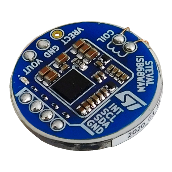
The STEVAL-ISB68WA is an evaluation kit based on STWLC68JRH wireless power receiver and it is designed as reference
solution for wearable applications. The kit consists of a wireless receiver module and USB-to-I2C bridging dongle. The receiver
is a 3-elements stack: a PCB housing the STWLC68JRH wireless power receiver and all the required external components, a 2
mm thick plastic spacer and a 15 mm diameter receiving coil facing the bottom side.
Figure 1.
Receiver module
The module is configured to provide a constant 5 V output voltage with a maximum power capability of 2.5 W and it works out of
the box when placed on a suitable wireless power transmitter.An on-board LED indicates when the communication with the
transmitter succeeds and the power transfer is in progress.Thanks to the I2C interface, the module can be easily controlled and
configured through the dedicated Graphical User Interface (GUI) by using the enclosed USB-to-I2C dongle.
The complete reference application is confined in a 10x10 mm area of the PCB and all the components are intentionally spaced
to ease probing and customization to the end user.
UM2693 - Rev 1 - February 2020
www.st.com
For further information contact your local STMicroelectronics sales office.
Advertisement
Table of Contents

Related Manuals for ST STEVAL-ISB68WA


Summary of Contents for ST STEVAL-ISB68WA
-
Page 1: Figure 1. Receiver Module
Introduction The STEVAL-ISB68WA is an evaluation kit based on STWLC68JRH wireless power receiver and it is designed as reference solution for wearable applications. The kit consists of a wireless receiver module and USB-to-I2C bridging dongle. The receiver is a 3-elements stack: a PCB housing the STWLC68JRH wireless power receiver and all the required external components, a 2 mm thick plastic spacer and a 15 mm diameter receiving coil facing the bottom side. -
Page 2: Wireless Power Receiver Module
UM2693 Wireless power receiver module Wireless power receiver module Overview As visible in Figure 2, the schematic diagram of the wireless power receiver is relatively simple. The RX coil (J1- J2 terminal) is part of the series resonant circuit (C1 through C4 capacitors) that provides the AC voltage to the AC1-AC2 pins of the STWLC68JRH. -
Page 3: Table 1. Receiver Module Terminals
UM2693 Wireless power receiver module The terminals for the receiving coil, the output load and the control signals are summarized in Table 1. The output rail and the control interface are already made easily accessible by means of wires terminated with pin header female connectors (Figure Table 1. -
Page 4: Table 2. Receiver Module Default Settings
UM2693 Wireless power receiver module Figure 4. Receiver module wiring Additional control signals and programmable general-purpose I/O pins are available at the STWLC68JRH, but they are not used in the module to keep the reference solution as simple as possible. The STWLC68JRH chip can handle up to 400 kHz speed over the I2C bus. -
Page 5: Table 3. Receiver Module Bill Of Material
UM2693 Wireless power receiver module As already mentioned, a LED (D3) is connected to GPIO0 and it is used as output state monitor: it turns-on when a correct power transfer is established between the receiving module and the transmitter, and the output voltage is enabled. -
Page 6: Usb To I2C Bridging Dongle
UM2693 USB to I2C bridging dongle USB to I2C bridging dongle Overview The USB to I2C bridging dongle is the tool that allows interfacing the receiver to the Graphical User Interface running on a PC. The P2 connector signals are summarized in Table 4. -
Page 7: Table 5. Usb-To-I2C Bridging Dongle Bill Of Material
UM2693 USB to I2C bridging dongle Signal Description Auxiliary supply rail. Used to supply the STWLC68JRH chip via VOUT when the receiver module is not placed on a transmitter. The D4 diode (see VBUS Figure 6) avoids backflow toward the USB supply rail when VOUT is higher than 5V. - Page 8 UM2693 USB to I2C bridging dongle Component Value Description Part Number Manufacturer Pin header, 2.54 mm pitch 3.3V, 100 mA, Linear LD2981CM33TR STMicroelectronics regulator, SOT23-5L Fuse, 0.25A, 0603 0603L025 Littelfuse USB to I2C MCP2221A-I/ML Microchip converter, QFN16 Linear regulator, 3.3V, 100 mA, LD2981CM33TR STMicroelectronics SOT23-5L...
-
Page 9: Steval-Isb68Wa Test Setup
STEVAL-ISB68WA test setup STEVAL-ISB68WA test setup The evaluation of the STEVAL-ISB68WA kit relies on a suitable wireless power transmitter that could mate with the coil of the RX module. A good coupling factor is essential for both power transfer efficiency and data communication reliability between the transmitter and the receiver. -
Page 10: Figure 9. Configuration Of The Transmitter
UM2693 STEVAL-ISB68WA test setup Figure 9. Configuration of the transmitter As soon as the LED on the receiver lights up, its control GUI can be launched. Connectivity with the STWLC68JRH is automatically verified and the chip info (IDs content) is shown in the registers page (Figure 10). -
Page 11: Figure 10. Graphical User Interface Registers Page Showing Chip Ids
UM2693 STEVAL-ISB68WA test setup Figure 10. Graphical User Interface registers page showing chip IDs To monitor the operation of the receiver, a real-time plotting of key parameters can be selected: in Figure 11 VRECT and VOUT voltages, the temperature of the rectifier (TRECT) and its output current (ISNS) are shown. -
Page 12: Figure 12. Changing The Output Voltage To 6 V Via Gui
UM2693 STEVAL-ISB68WA test setup The load at VOUT can be increased up to 2.5 W. A 10 Ω purely resistive load (i.e. 2.5 W load at 5 V) is usually managed without problems also at ping-up. In some case (e.g. a following DC-DC converter stage) the load could show a remarkable capacitive behavior and a relatively high initial current may trigger the over-current protection or may exceed the dynamic capability of the transmitter. -
Page 13: Figure 13. Transmitter Input To Receiver Output Overall Efficiency
UM2693 STEVAL-ISB68WA test setup Figure 13. Transmitter input to receiver output overall efficiency UM2693 - Rev 1 page 13/18... -
Page 14: Revision History
UM2693 Revision history Table 6. Document revision history Date Version Changes 19-Feb-2020 Initial release. UM2693 - Rev 1 page 14/18... -
Page 15: Table Of Contents
STEVAL-ISB68WA test setup ........ -
Page 16: List Of Tables
UM2693 List of tables List of tables Table 1. Receiver module terminals ............. 3 Table 2. -
Page 17: List Of Figures
STEVAL-ISB68WA evaluation setup ........ - Page 18 ST’s terms and conditions of sale in place at the time of order acknowledgement. Purchasers are solely responsible for the choice, selection, and use of ST products and ST assumes no liability for application assistance or the design of Purchasers’...
Need help?
Do you have a question about the STEVAL-ISB68WA and is the answer not in the manual?
Questions and answers