Table of Contents
Advertisement
Quick Links
Advertisement
Table of Contents

Related Manuals for National Instruments PXIe-6591R


Summary of Contents for National Instruments PXIe-6591R
- Page 1 Artisan Technology Group is your source for quality new and certified-used/pre-owned equipment SERVICE CENTER REPAIRS WE BUY USED EQUIPMENT • FAST SHIPPING AND DELIVERY Experienced engineers and technicians on staff Sell your excess, underutilized, and idle used equipment at our full-service, in-house repair center We also offer credit for buy-backs and trade-ins •...
- Page 2 NI High-Speed Serial Instruments User Manual PXIe-6591R PXIe-6592R PXIe-7902 NI High-Speed Serial Instruments User Manual June 2017 374574F-01 Artisan Technology Group - Quality Instrumentation ... Guaranteed | (888) 88-SOURCE | www.artisantg.com...
- Page 3 11500 North Mopac Expressway Austin, Texas 78759-3504 USA Tel: 512 683 0100 For further support information, refer to the NI Services appendix. To comment on National Instruments documentation, refer to the National Instruments website at ni.com/info enter the Info Code feedback ©...
- Page 4 National Instruments Corporation. National Instruments respects the intellectual property of others, and we ask our users to do the same. NI software is protected by copyright and other intellectual property laws. Where NI software may be used to reproduce software or other materials belonging to others, you may use NI software only to reproduce materials that you may reproduce in accordance with the terms of any applicable license or other legal restriction.
- Page 5 The ExpressCard ™ word mark and logos are owned by PCMCIA and any use of such marks by National Instruments is under license. The mark LabWindows is used under a license from Microsoft Corporation. Windows is a registered trademark of Microsoft Corporation in the United States and other countries.
- Page 6 Operation of this hardware in a residential area is likely to cause harmful interference. Users are required to correct the interference at their own expense or cease operation of the hardware. Changes or modifications not expressly approved by National Instruments could void the user’s right to operate the hardware under the local regulatory rules.
-
Page 7: Table Of Contents
PXIe-6591R Hardware Architecture PXIe-6591R Module Overview..................2-2 Clocking Architecture....................2-3 PXIe-6591R Clocking ....................2-3 Chapter 3 Connecting and Interfacing with the PXIe-6591R Front Panel........................3-1 Recommended Mating Cables and Connectors..............3-2 Transceiver Lane and Quad Mapping ................3-2 Signal Routing ........................3-3 Socketed CLIP Interface.................... - Page 8 Contents Chapter 6 PXIe-7902 Hardware Architecture PXIe-7902 Module Overview...................6-2 Clocking Architecture....................6-3 PXIe-7902 Clocking ....................6-3 Chapter 7 Connecting and Interfacing with the PXIe-7902 Front Panel ........................7-1 Recommended Mating Cables and Connectors ..............7-2 Transceiver Lane and Quad Mapping................7-2 Signal Routing ........................
- Page 9 Figure 2-1. PXIe-6591R System Architecture Elements ......... 2-2 Figure 2-2. PXIe-6591R Clocking Diagram ............2-4 Figure 3-1. PXIe-6591R Front Panel Connectors and Pinouts ........ 3-1 Figure 3-2. PXIe-6591R Signal Routing..............3-3 Figure 3-3. PXIe-6591R Socketed CLIP Diagram ..........3-4 Figure 4-1.
- Page 10 Fundamentals Resources ...............1-1 Table 2-1. PXIe-6591R Key Features..............2-2 Table 2-2. PXIe-6591R Reference Clocks.............. 2-3 Table 3-1. PXIe-6591R Front Panel Connectors ............ 3-2 Table 3-2. Transceiver Lane and Quad Mapping ...........3-2 Table 3-3. Clock Signal and Quad Mapping............3-3 Table 3-4.
- Page 11 Clock Signal and Quad Mapping ............7-3 Table 7-4. PXIe-7902 Socketed CLIP Signals ............7-4 Table 8-1. PXIe-6591R Clocking and Routing Dependencies ....... 8-11 Table 8-2. NI 6592R Clocking and Routing Dependencies ........8-12 Table B-1. Xilinx 7-Series FPGA Documentation..........B-1 ©...
-
Page 12: About This Manual
About This Manual The NI High-Speed Serial Instruments User Manual describes how to develop applications for use with the PXIe-6591R, PXIe-6592R, and PXIe-7902 high-speed serial FPGA targets. The PXIe-6591R, PXIe-6592R, and PXIe-7902 are designed for use in the following applications: •... - Page 13 About This Manual Table 1. Documentation Locations and Descriptions (Continued) Document Location Description PXIe-6592R Getting Started Available from the Start Contains installation Guide menu and at instructions for your ni.com/ system. manuals PXIe-7902 Getting Started Guide Available from the Start Contains installation menu and at instructions for your...
- Page 14 LabVIEW FPGA Module, Release and selecting Start»All describes new features, and Upgrade Programs»National provides upgrade Notes Instruments» information. LabVIEW» LabVIEW Manuals. © National Instruments | 13 Artisan Technology Group - Quality Instrumentation ... Guaranteed | (888) 88-SOURCE | www.artisantg.com...
-
Page 15: Xilinx Documentation
About This Manual Xilinx Documentation Xilinx FPGA documentation provides information required for the successful development of your high-speed serial device. The following table provides a list of specific Xilinx documentation resources. All Xilinx documentation can be found at www.xilinx.com Table 2. Xilinx Documentation Document Part Document Number... -
Page 16: Before You Begin
NI LabVIEW and LabVIEW FPGA training are available at . You can also ni.com/training refer to the NI LabVIEW High-Performance FPGA Developer’s Guide, available at ni.com/ tutorial © National Instruments | 1-1 Artisan Technology Group - Quality Instrumentation ... Guaranteed | (888) 88-SOURCE | www.artisantg.com... -
Page 17: Xilinx Licensing Information
Chapter 1 Before You Begin Xilinx Licensing Information Refer to the Xilinx Documentation section in About This Manual for a list of Xilinx documentation that contains important Xilinx licensing information. Installation Instructions Refer to the getting started guide for your device (refer to the Related Documentation section of this document) for instructions about how to install LabVIEW, LabVIEW FPGA, the... -
Page 18: Pxie-6591R Hardware Architecture
PXIe-6591R-based projects consist of the following key components: • PXIe-6591R front panel connectors for data, clocking, and triggering external to the module • Socketed CLIP for HDL IP and interface definition from the FPGA VI to the PXIe-6591R front panel • Xilinx Kintex-7 FPGA •... -
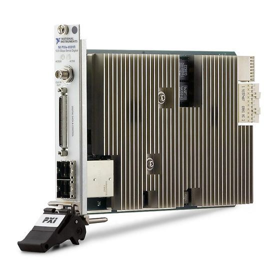
Page 19: Pxie-6591R Module Overview
FPGA VI Host VI DRAM PXIe-6591R Module Overview The PXIe-6591R module includes the following key features. Refer to the PXIe-6591R Specifications for more details. Table 2-1. PXIe-6591R Key Features Line rate 500 Mb/s to 8 Gb/s and 9.8 Gb/s to 12.5 Gb/s... -
Page 20: Clocking Architecture
NI High-Speed Serial Instruments User Manual Clocking Architecture The PXIe-6591R module includes dedicated clocking hardware to provide a flexible clocking solution for generating the high-speed serial transceiver reference clocks (MGT_RefClk). Use the Clocking and IO properties page in the LabVIEW project to configure the clock settings for your module. -
Page 21: Figure 2-2. Pxie-6591R Clocking Diagram
Chapter 2 PXIe-6591R Hardware Architecture The following figure illustrates the clocking circuitry on the PXIe-6591R. Figure 2-2. PXIe-6591R Clocking Diagram CLK IN/OUT PXIe_Clk100 Clock Synthesis PXIe_DStarA Routing MGT_RefClk0 PORT 0 MGT_RefClk1 FPGA PORT 1 2-4 | ni.com Artisan Technology Group - Quality Instrumentation ... Guaranteed | (888) 88-SOURCE | www.artisantg.com... -
Page 22: Connecting And Interfacing With The Pxie-6591R
Connecting and Interfacing with the PXIe-6591R This chapter contains information about the PXIe-6591R module and its functionality, including front panel diagrams, connectors, and pinouts. Front Panel The following figure shows the pinouts for the PXIe-6591R front panel connectors. Figure 3-1. PXIe-6591R Front Panel Connectors and Pinouts RESERVED Optical 3.3 V... -
Page 23: Recommended Mating Cables And Connectors
Chapter 3 Connecting and Interfacing with the PXIe-6591R Refer to the following table for a list of the PXIe-6591R front panel connectors and their descriptions. Table 3-1. PXIe-6591R Front Panel Connectors Connector Type Description CLK IN/OUT Reference Clock input and exported clock output Digital Data &... -
Page 24: Signal Routing
Clocks for single or multiple transceivers. Signal Routing The PXIe-6591R high-speed serial differential signals are routed directly from the Kintex-7 FPGA pins to the PORT 0 and PORT 1 connector pins using a 100 nF AC-coupling capacitor, as shown in the following figure. -
Page 25: Pxie-6591R Socketed Clip
Chapter 3 Connecting and Interfacing with the PXIe-6591R PXIe-6591R Socketed CLIP Refer to the following diagram for an overview of the PXIe-6591R socketed CLIP interface. Figure 3-3. PXIe-6591R Socketed CLIP Diagram PXIe-6591R Clock Xilinx Kintex-7 FPGA Synthesis and Routing Socketed CLIP... - Page 26 NI High-Speed Serial Instruments User Manual Table 3-4. PXIe-6591R CLIP Signals (Continued) Clock Port Direction Domain Description MGT_RefClks_ Async Indicates the state of the PLL ExtPllLocked within the clocking logic that provides the Reference Clock to the FPGA MGTs (MGT_ RefClkx signals).
- Page 27 Chapter 3 Connecting and Interfacing with the PXIe-6591R Table 3-4. PXIe-6591R CLIP Signals (Continued) Clock Port Direction Domain Description ExportedUser Clock Reserved for future use. ReferenceClk LED_ActiveRed Async The front panel Active indicator’s red LED turns on when this signal is driven high.
- Page 28 NI High-Speed Serial Instruments User Manual Table 3-4. PXIe-6591R CLIP Signals (Continued) Clock Port Direction Domain Description LED_ActiveGreen Async The front panel Active indicator’s green LED turns on when this signal is driven high. The CLIP’s access to this LED...
- Page 29 Chapter 3 Connecting and Interfacing with the PXIe-6591R Table 3-4. PXIe-6591R CLIP Signals (Continued) Clock Port Direction Domain Description sFrontEndConfiguration SocketClk40 Asserts high and stays high Done when the power-on self-configuration (POSC) state machine is finished with configuration. After the aResetSl signal...
- Page 30 NI High-Speed Serial Instruments User Manual Table 3-4. PXIe-6591R CLIP Signals (Continued) Clock Port Direction Domain Description aResetSl Async This signal is not required. This signal is an asynchronous reset signal from the LabVIEW FPGA environment. If you create an input signal to your...
- Page 31 Chapter 3 Connecting and Interfacing with the PXIe-6591R Table 3-4. PXIe-6591R CLIP Signals (Continued) Clock Port Direction Domain Description Port<0..1>_SDA In/Out Async Bidirectional serial data signal for the two-wire communication interface on the Port <0..1> connector. Valid values: 0 and Z (open drain).
- Page 32 NI High-Speed Serial Instruments User Manual Table 3-4. PXIe-6591R CLIP Signals (Continued) Clock Port Direction Domain Description DDC_GPIO_In(19:0) Async These signals are GPIO inputs within the DDC VHDCI connector. These signals, along with DDC_GPIO_Out(19:0) and DDC_GPIO_OutEnable_ n(19:0), allow control and...
-
Page 33: Pxie-6592R Hardware Architecture
• Xilinx Kintex-7 FPGA • Dynamic random access memory (DRAM) • NI-defined bus interface from the FPGA to the host PC © National Instruments | 4-1 Artisan Technology Group - Quality Instrumentation ... Guaranteed | (888) 88-SOURCE | www.artisantg.com... -
Page 34: Pxie-6592R Module Overview
Chapter 4 PXIe-6592R Hardware Architecture The following figure illustrates the key components of the PXIe-6592R architecture. Figure 4-1. PXIe-6592R System Architecture Elements PXIe-659xR Host PC Xilinx Kintex-7 FPGA • DMA FIFOs DDC / PFI • Controls • Indicators Front Panel Connectors High Speed LabVIEW... -
Page 35: Clocking Architecture
60 MHz to 670 MHz Backplane: PXIe_Clk100 and PXIe_DStarA MGT_RefClk1 Front panel: PFI 0/CLK IN/OUT Other: 10 MHz Onboard Clock MGT_RefClk2 156.25 MHz — © National Instruments | 4-3 Artisan Technology Group - Quality Instrumentation ... Guaranteed | (888) 88-SOURCE | www.artisantg.com... -
Page 36: Figure 4-2. Pxie-6592R Clocking Diagram
Chapter 4 PXIe-6592R Hardware Architecture Table 4-4. PXIe-6592R Reference Clocks Frequency Clock Name Range Available Sources MGT_RefClk0 60 MHz to Backplane: PXIe_Clk100 and PXIe_DStarA 700 MHz Front panel: CLK IN/OUT MGT_RefClk1 Refer to the Configuring the High-Speed Serial Device LabVIEW FPGA Targets section of Chapter 8, Developing Applications for the High-Speed Serial... -
Page 37: Connecting And Interfacing With The Pxie-6592R
ACCESS ACTIVE VeeR VeeR PFI 0 PFI 1 RD– Rx_LOS VeeR VccR MOD_ABS VccT VeeT Tx_Disable TD– Tx_Fault VeeT 20 1 VeeT © National Instruments | 5-1 Artisan Technology Group - Quality Instrumentation ... Guaranteed | (888) 88-SOURCE | www.artisantg.com... -
Page 38: Recommended Mating Cables And Connectors
Chapter 5 Connecting and Interfacing with the PXIe-6592R Refer to the following table for a list of the PXIe-6592R front panel connectors and their descriptions. Table 5-1. PXIe-6592R Front Panel Connectors Connector Type Description PFI 0/CLK IN/OUT Reference Clock input, exported clock output, and general-purpose PFI 1/CLK OUT I/O. -
Page 39: Signal Routing
FPGA. The following sections provide information about how to configure your device for use with socketed CLIP. © National Instruments | 5-3 Artisan Technology Group - Quality Instrumentation ... Guaranteed | (888) 88-SOURCE | www.artisantg.com... -
Page 40: Pxie-6592R Socketed Clip
Chapter 5 Connecting and Interfacing with the PXIe-6592R PXIe-6592R Socketed CLIP Refer to the following diagram for an overview of the PXIe-6592R socketed CLIP interface. Figure 5-3. PXIe-6592R Socketed CLIP Diagram PXIe-6592R Clock Xilinx Kintex-7 FPGA Synthesis and Routing LabVIEW FPGA VI High-Speed Serial MGT_RefClks Protocol IP... - Page 41 Using Frequency Counters section of Chapter 8, Developing Applications for the High-Speed Serial Device, for details about how to use these signals. © National Instruments | 5-5 Artisan Technology Group - Quality Instrumentation ... Guaranteed | (888) 88-SOURCE | www.artisantg.com...
- Page 42 Chapter 5 Connecting and Interfacing with the PXIe-6592R Table 5-4. PXIe-6592R CLIP Signals (Continued) Clock Port Direction Domain Description ExportedUser Clock Reserved for future use. ReferenceClk LED_ActiveRed Async The front panel Active indicator’s red LED turns on when this signal is driven high. The CLIP’s access to this LED may be temporarily overridden to show error conditions,...
- Page 43 This signal is connected to the 40 MHz Onboard Clock signal, which is the default top-level clock for the LabVIEW FPGA VI. © National Instruments | 5-7 Artisan Technology Group - Quality Instrumentation ... Guaranteed | (888) 88-SOURCE | www.artisantg.com...
- Page 44 Chapter 5 Connecting and Interfacing with the PXIe-6592R Table 5-4. PXIe-6592R CLIP Signals (Continued) Clock Port Direction Domain Description sFrontEnd SocketClk40 Asserts high and stays high when ConfigurationDone the power-on self-configuration (POSC) state machine is finished with configuration. After the aResetSl signal transitions from high to low, indicating that the CLIP logic should come out of reset, a POSC...
- Page 45 This signal is grounded when a module is connected to indicate that the module is present. This signal is pulled asserted when no module is present. © National Instruments | 5-9 Artisan Technology Group - Quality Instrumentation ... Guaranteed | (888) 88-SOURCE | www.artisantg.com...
- Page 46 Chapter 5 Connecting and Interfacing with the PXIe-6592R Table 5-4. PXIe-6592R CLIP Signals (Continued) Clock Port Direction Domain Description Port<0..3>_RS0 Async Drives the Port <0..3> SFP+ module’s RX rate select signal. If this signal’s RX rate is more than 4.25 Gbps, drive this signal high.
- Page 47 Enables or disables the optical Power power supply on Port <0..3>. Assert this signal to enable the optical supply for its corresponding port. © National Instruments | 5-11 Artisan Technology Group - Quality Instrumentation ... Guaranteed | (888) 88-SOURCE | www.artisantg.com...
- Page 48 Chapter 5 Connecting and Interfacing with the PXIe-6592R Table 5-4. PXIe-6592R CLIP Signals (Continued) Clock Port Direction Domain Description sPort<0..3>_Power SocketClk40 Indicates that the optical power Good supply for Port <0..3> is enabled. This signal may deassert if an over-power condition occurs. PFI<0..3>_GPIO_In Async Acquires GPIO input from the...
- Page 49 • Xilinx Virtex-7 FPGA • Dynamic random access memory (DRAM) • NI-defined bus interface from the FPGA to the host PC © National Instruments | 6-1 Artisan Technology Group - Quality Instrumentation ... Guaranteed | (888) 88-SOURCE | www.artisantg.com...
-
Page 50: Pxie-7902 Hardware Architecture
Chapter 6 PXIe-7902 Hardware Architecture The following figure illustrates the key components of the PXIe-7902 architecture. Figure 6-1. PXIe-7902 System Architecture Elements PXIe-7902 Host PC Xilinx Virtex-7 FPGA • DMA FIFOs • Controls • Indicators Front Panel Connectors High Speed LabVIEW PXI Triggers Serial IO... -
Page 51: Clocking Architecture
Chapter 8, Developing Applications for the High-Speed Serial Device, for more information about how to configure Reference Clocks for your device. © National Instruments | 6-3 Artisan Technology Group - Quality Instrumentation ... Guaranteed | (888) 88-SOURCE | www.artisantg.com... - Page 52 Chapter 6 PXIe-7902 Hardware Architecture The following figure illustrates the clocking circuitry on the PXIe-7902. Figure 6-2. PXIe-7902 Clocking Diagram CLK IN MGT_RefClk0 PXIe_Clk100 Clock PORT 0 MGT_RefClk1 Synthesis PXIe_DStarA PORT 1 MGT_RefClk2 Routing PORT 2 PORT 3 FPGA PORT 4 PORT 5 6-4 | ni.com Artisan Technology Group - Quality Instrumentation ...
-
Page 53: Front Panel
EEPROM 3.3 V Tx+ 1 Tx+ 0 Tx– 1 Tx– 0 Tx+ 3 Tx+ 2 Tx– 3 Tx– 2 x6 (1 per Port) © National Instruments | 7-1 Artisan Technology Group - Quality Instrumentation ... Guaranteed | (888) 88-SOURCE | www.artisantg.com... -
Page 54: Recommended Mating Cables And Connectors
Chapter 7 Connecting and Interfacing with the PXIe-7902 Refer to the following table for a list of the PXIe-7902 front panel connectors and their descriptions. Table 7-1. PXIe-7902 Front Panel Connectors Connector Type Description CLK IN Reference Clock input and general-purpose I/O Port 0 Mini-SAS HD x4... -
Page 55: Signal Routing
FPGA. The following sections provide information about how to configure your device for use with socketed CLIP. © National Instruments | 7-3 Artisan Technology Group - Quality Instrumentation ... Guaranteed | (888) 88-SOURCE | www.artisantg.com... -
Page 56: Pxie-7902 Socketed Clip
Chapter 7 Connecting and Interfacing with the PXIe-7902 PXIe-7902 Socketed CLIP Refer to the following diagram for an overview of the PXIe-7902 socketed CLIP interface. Figure 7-3. PXIe-7902 Socketed CLIP Diagram PXIe-7902 Clock Xilinx Virtex-7 FPGA Synthesis and Routing LabVIEW FPGA VI High-Speed Serial MGT_RefClks Protocol IP... - Page 57 This signal is connected to the 40 MHz Onboard Clock signal, which is the default top-level clock for the LabVIEW FPGA VI. © National Instruments | 7-5 Artisan Technology Group - Quality Instrumentation ... Guaranteed | (888) 88-SOURCE | www.artisantg.com...
- Page 58 Chapter 7 Connecting and Interfacing with the PXIe-7902 Table 7-4. PXIe-7902 Socketed CLIP Signals (Continued) Clock Port Direction Domain Description Port<0..5>_SCL In/Out Async Bidirectional serial clock signal for the two wire communication interface on the Port<0..5> connector. Valid values are 0 and Z (open drain).
- Page 59 Connections Using Eye Scan section of Chapter 8, Developing Applications for the High-Speed Serial Device, for details about how to use these signals. © National Instruments | 7-7 Artisan Technology Group - Quality Instrumentation ... Guaranteed | (888) 88-SOURCE | www.artisantg.com...
- Page 60 Chapter 7 Connecting and Interfacing with the PXIe-7902 Table 7-4. PXIe-7902 Socketed CLIP Signals (Continued) Clock Port Direction Domain Description ExportedUser Clock Reserved for future use. ReferenceClk sFrontEnd SocketClk40 Asserts high and stays high when ConfigurationDone the power-on self-configuration (POSC) state machine is finished with configuration.
- Page 61 SocketClk40 Indicates that the optical power Good supply for Port <0..5> is enabled. This signal may deassert if an over-power condition occurs. © National Instruments | 7-9 Artisan Technology Group - Quality Instrumentation ... Guaranteed | (888) 88-SOURCE | www.artisantg.com...
-
Page 62: Developing Applications For The High-Speed Serial Device
You can develop socketed CLIP either by using the Xilinx Vivado tools, or by exporting a LabVIEW FPGA VI as a Vivado Design Suite project. © National Instruments | 8-1 Artisan Technology Group - Quality Instrumentation ... Guaranteed | (888) 88-SOURCE | www.artisantg.com... -
Page 63: Accessing The Xilinx Vivado Tools
Chapter 8 Developing Applications for the High-Speed Serial Device • The Xilinx Vivado tools create a blank project, from which you can develop socketed CLIP. For more information about using the Xilinx Vivado tools to develop socketed CLIP, refer to the Accessing the Xilinx Vivado Tools section. -
Page 64: Exporting To Vivado
Refer to the Exporting FPGA VIs as Vivado Design Suite Projects (FPGA Module) topic in the LabVIEW Help for more information about this feature. The PXIe-6591R, PXIe-6592R, and PXIe-7902 devices support exporting to Vivado. The Aurora sample projects for the PXIe-6591R, PXIe-6592R, and PXIe-7902R provide out-of-the-box support that demonstrates how to use hardware design files as an entry point when exporting to Vivado. - Page 65 Chapter 8 Developing Applications for the High-Speed Serial Device FPGA files, the unencrypted design files with the prefix, and the Vivado project UserRTL_ files. Open the Vivado project using the file. LaunchVivadoDesignSuite.bat The source hierarchy loads once Vivado launches. The hierarchy source is encrypted, except for the design files prefixed with Note and added to the FPGA target as a socketed CLIP.
-
Page 66: Generating An Ip Core From The Xilinx Vivado Ip Catalog
Include Shared Logic in example design in the IP wizard. The image on the right in Figure 8-3 shows this option. © National Instruments | 8-5 Artisan Technology Group - Quality Instrumentation ... Guaranteed | (888) 88-SOURCE | www.artisantg.com... -
Page 67: Building A Netlist From The Ip Core
Chapter 8 Developing Applications for the High-Speed Serial Device Do not modify the IP core unless you understand the required reference Note clock(s) and clocking resources. The following figure shows the difference between the top-level CLIP VHDL with shared logic in the core (left) and without shared logic (right). - Page 68 Copy the netlist into your LabVIEW FPGA CLIP directory. Include your netlist in the list of synthesis files when running the CLIP Wizard. © National Instruments | 8-7 Artisan Technology Group - Quality Instrumentation ... Guaranteed | (888) 88-SOURCE | www.artisantg.com...
-
Page 69: Writing A Vhdl Wrapper Around The Protocol Ip Core
Chapter 8 Developing Applications for the High-Speed Serial Device Writing a VHDL Wrapper Around the Protocol IP Core A VHDL wrapper is generally necessary to adapt the protocol signals to the dataflow semantics used within the LabVIEW FPGA diagram. NI recommends that you adhere to the following guidelines when writing a VHDL wrapper around the protocol IP core: •... -
Page 70: Constraints And Hierarchy
CLIP are written in the same clock domain in which they are read on the LabVIEW diagram and that I/O nodes to the CLIP are read in the same clock © National Instruments | 8-9 Artisan Technology Group - Quality Instrumentation ... Guaranteed | (888) 88-SOURCE | www.artisantg.com... -
Page 71: Documenting Your Ip
Chapter 8 Developing Applications for the High-Speed Serial Device domain in which they are written on the LabVIEW diagram. In rare cases where crossing clock domains is desirable, refer to KnowledgeBase 6OB8E8FM for more information about how to write timing constraints between the ni.com/kb CLIP and the LabVIEW diagram in order to specify timing exceptions on these paths and achieve timing closure. -
Page 72: Developing With Labview Fpga
Specifying how to use the signals in your CLIP In Step 2 of the CLIP Wizard, select the appropriate Component Level IP Note Type for your target. © National Instruments | 8-11 Artisan Technology Group - Quality Instrumentation ... Guaranteed | (888) 88-SOURCE | www.artisantg.com... - Page 73 CLIP for use with your application. When CLK IN/OUT is enabled as an output reference Note (PXIe-6591R only) clock, it routes the specified frequency to the SMA connector. When PFI 0/CLK OUT, PFI 1, PFI 2, and PFI 3 are...
- Page 74 15. Under GPIO Configuration, use the Voltage Family selector box to specify the voltage level used by the GPIO (Digital Data and Control on the PXIe-6591R, and PFI 0, PFI 1, PFI 2, and PFI 3 on the PXIe-6592R).
- Page 75 Chapter 8 Developing Applications for the High-Speed Serial Device Table 8-2. PXIe-6592R Clocking and Routing Dependencies Connector/Clock Valid Configurations Notes PFI 0/CLK IN Input clock or output clock When enabled as output clocks, PFI 0/CLK IN/OUT, PFI 1/ CLK OUT, PFI 2/CLK OUT, and PFI 3/CLK OUT must share the same frequency.
-
Page 76: Using Existing Vhdl Ip Inside Clip Or Ipin
By selecting an input clock and an output clock in this example, the Note MGT_RefClk0 is phase loop-locked to the incoming 100 MHz clock. Refer to Chapter 2, PXIe-6591R Hardware Architecture, for more information about PXIe-6591R clocking capabilities. Refer to Chapter 4, PXIe-6592R Hardware Architecture, for more information about PXIe-6592R clocking capabilities. -
Page 77: Using The Ni Common Instrument Design Libraries
Chapter 8 Developing Applications for the High-Speed Serial Device To remove a resource, select the resource under New FPGA I/O and click the left arrow button. Click OK. Using the NI Common Instrument Design Libraries Instrument design libraries can speed up your application development. The instrument design libraries are located at <LVDir>\instr.lib\_niInstr In LabVIEW, the common instrument design libraries are located on the niHighSpeedSerial... - Page 78 Instruction Producer, such as the FIFO Register Bus library, instead of using controls and indicators on the top level of the FPGA diagram. © National Instruments | 8-17 Artisan Technology Group - Quality Instrumentation ... Guaranteed | (888) 88-SOURCE | www.artisantg.com...
-
Page 79: Using Niinstr Streaming
Chapter 8 Developing Applications for the High-Speed Serial Device Using niInstr Streaming The Streaming Instrument Design Library provides a consistent mechanism to handle both finite and continuous transfer streams. It provides stream monitoring and handshaking. It contains VIs for both the Host and FPGA. Refer to the Aurora Simple Streaming sample project for an example of how to use the Streaming Instrument Design Library. -
Page 80: Connecting Signals To Enable Eye Scan
Instruction Framework using the Create AXI4-Lite Resources VI. The Create AXI4-Lite Resources VI creates the AXI4-Lite CLIP Adapter and specifies the offsets for the DRP © National Instruments | 8-19 Artisan Technology Group - Quality Instrumentation ... Guaranteed | (888) 88-SOURCE | www.artisantg.com... - Page 81 Chapter 8 Developing Applications for the High-Speed Serial Device registers. The DRP subsystems in that VI are then registered with the Instruction Framework via the call to Add Subsystems.vi. Figure 8-6. Connecting CLIP Resources to the Instruction Framework The following figure shows Create AXI4-Lite Resources.vi, which is used by each Aurora sample project.
-
Page 82: Compiling Labview Fpga Vis
When the clocking configuration is in an indeterminate state, you cannot rely on clocking stability from the clocking and routing hardware on the high-speed serial device. © National Instruments | 8-21 Artisan Technology Group - Quality Instrumentation ... Guaranteed | (888) 88-SOURCE | www.artisantg.com... -
Page 83: Dma Streaming
Chapter 8 Developing Applications for the High-Speed Serial Device DMA Streaming The high-speed serial devices support both host-to-target streaming and target-to-host streaming through DMA channels that connect the host to your target. Use DMA streaming to allow the maximum throughput of data from your host application to be streamed to the target at high rates of speed. -
Page 84: Peer-To-Peer Streaming
12.5 nanoseconds, the trigger line must be constant for at least 25 ns, which is two cycles of an 80 MHz clock. © National Instruments | 8-23 Artisan Technology Group - Quality Instrumentation ... Guaranteed | (888) 88-SOURCE | www.artisantg.com... -
Page 85: Reserving Pxi Triggers
Reserving PXI Triggers National Instruments recommends that you reserve the trigger lines used by PXI devices, including the high-speed serial device. If two PXI devices try to drive the same trigger line in different applications, or if the PXI devices are not programmed to work together, the application does not work, and in some cases, third-party PXI devices can be damaged. -
Page 86: Releasing Trigger Lines
Read Module Temperature allows you to read two onboard sensors: one sensor is embedded directly in the FPGA, and one reads the device temperature. Figure 8-8. Read Module Temperature © National Instruments | 8-25 Artisan Technology Group - Quality Instrumentation ... Guaranteed | (888) 88-SOURCE | www.artisantg.com... -
Page 87: Soft Shutdown
Chapter 8 Developing Applications for the High-Speed Serial Device Read Module Power provides information about how much power the device is drawing from the chassis 3.3V and 12V power rails. Figure 8-9. Read Module Power Soft Shutdown Exceeding the soft thermal and power threshold puts your device in a safe state and provides a warning. -
Page 88: Debugging Link Connections Using Eye Scan
Refer to the Aurora sample project to learn how to use the Eye Scan API in an application. National Instruments offers two versions of Eye Scan: Rectangular Eye Scan and N Point Eye Scan. Use Rectangular Eye Scan to obtain a traditional eye that sweeps the unit interval and nominal voltage. -
Page 89: N Point Eye Scan
Chapter 8 Developing Applications for the High-Speed Serial Device N Point Eye Scan The following portion of code shows a typical use case for N Point Eye Scan. This code scans 4 points with a Bit Error Ratio floor of 2.33E-10 and produces a 4-point eye, which is useful for measuring pass/fail conditions. -
Page 90: Eye Scan State Model
Figure 8-12. Eye Scan State Model Configure Property Start Configure Property Stopped Stop Measure Open Session Start Uninitialized Measuring Done Finished Start Configure Property © National Instruments | 8-29 Artisan Technology Group - Quality Instrumentation ... Guaranteed | (888) 88-SOURCE | www.artisantg.com... - Page 91 Chapter 8 Developing Applications for the High-Speed Serial Device Complete the following steps to program the Eye Scan state model. Open a session with Open Session (Poly).vi. Configure the properties using the Property Node, located on the NI Eye Scan VI palette (FPGA Interface»Software-Designed Instruments»NI High-Speed Serial»NI Eye Scan).
- Page 92 6R6EOLM3 For information about troubleshooting problems adding your high-speed serial instrument to your Real Time system, refer to Knowledge Base article 7AEBF43J © National Instruments | A-1 Artisan Technology Group - Quality Instrumentation ... Guaranteed | (888) 88-SOURCE | www.artisantg.com...
-
Page 93: Xilinx Documentation References
FPGAs GTX/GTH transceivers. User Guide Vivado Design Suite User UG903 Describes using Xilinx Design Constraints Guide: Using Constraints (XDC) in Vivado tools. © National Instruments | B-1 Artisan Technology Group - Quality Instrumentation ... Guaranteed | (888) 88-SOURCE | www.artisantg.com... - Page 94 NI Services National Instruments provides global services and support as part of our commitment to your success. Take advantage of product services in addition to training and certification programs that meet your needs during each phase of the application life cycle; from planning and development through deployment and ongoing maintenance.
-
Page 95: Appendix Cni Services
Appendix C NI Services • Training and Certification—The NI training and certification program is the most effective way to increase application development proficiency and productivity. Visit for more information. ni.com/training – The Skills Guide assists you in identifying the proficiency requirements of your current application and gives you options for obtaining those skills consistent with your time and budget constraints and personal learning preferences. - Page 96 Dynamic random-access memory FPGA Field-programmble gate array GPIO General-purpose input/output High-speed serial Integrated circuit Intellectual property (VHDL/Verilog/Netlist) Loss of signal LVFPGA LabVIEW FPGA © National Instruments | G-1 Artisan Technology Group - Quality Instrumentation ... Guaranteed | (888) 88-SOURCE | www.artisantg.com...
- Page 97 Glossary Multi-gigabit transceiver Programmable function interface POSC Power on self-configuration SCTL Single cycle timed loop SFP+ Enhanced small form-factor pluggable G-2 | ni.com Artisan Technology Group - Quality Instrumentation ... Guaranteed | (888) 88-SOURCE | www.artisantg.com...
- Page 98 Artisan Technology Group is your source for quality new and certified-used/pre-owned equipment SERVICE CENTER REPAIRS WE BUY USED EQUIPMENT • FAST SHIPPING AND DELIVERY Experienced engineers and technicians on staff Sell your excess, underutilized, and idle used equipment at our full-service, in-house repair center We also offer credit for buy-backs and trade-ins •...
Need help?
Do you have a question about the PXIe-6591R and is the answer not in the manual?
Questions and answers