
Subscribe to Our Youtube Channel
Related Manuals for National Instruments PXIe-4340


Summary of Contents for National Instruments PXIe-4340
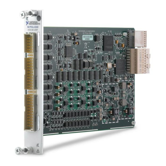
- Page 1 SC Express NI PXIe-4340 User Manual 4 Ch, 24-bit, 25.6 kS/s Simultaneous AC LVDT Input Module NI PXIe-4340 User Manual May 2016 377014A-01...
- Page 2 Tel: 866 ASK MYNI (275 6964) NI Services For further support information, refer to the appendix. To comment on National ni.com/info Instruments documentation, refer to the National Instruments website at feedback enter the Info Code © 2016 National Instruments. All rights reserved.
- Page 3 National Instruments Corporation. National Instruments respects the intellectual property of others, and we ask our users to do the same. NI software is protected by copyright and other intellectual property laws. Where NI software may be used to reproduce software or other materials belonging to others, you may use NI software only to reproduce materials that you may reproduce in accordance with the terms of any applicable license or other legal restriction.
- Page 4 ™ The ExpressCard word mark and logos are owned by PCMCIA and any use of such marks by National Instruments is under license. The mark LabWindows is used under a license from Microsoft Corporation. Windows is a registered trademark of Microsoft Corporation in the United States and other countries.
-
Page 5: Table Of Contents
Connecting Resolver Signals.................... 2-6 Connecting Synchro Signals..................... 2-6 Self-Calibration ........................ 2-7 Module Pinout ........................2-7 I/O Connector Signal Descriptions................2-9 PXIe-4340 Block Diagram ....................2-9 Open Coil Detection ....................2-10 Overcurrent Detection ....................2-11 Signal Acquisition Considerations ................... 2-11 Excitation Verification ..................... 2-11 Demodulation ...................... - Page 6 6-Wire Connection to an LVDT or RVDT..........2-5 Figure 2-6. Resolver Connections ................2-6 Figure 2-7. Synchro Connections ................2-6 Figure 2-8. PXIe-4340 Single-Channel Block Diagram .......... 2-10 Figure 2-9. HWTSP Data Path Model..............2-14 Figure 2-10. Transfer Time and Application Time Relationship ....... 2-14 Figure 2-11.
-
Page 7: Getting Started
Getting Started The NI PXIe-4340 provides four simultaneously sampled AC LVDT input channels. The PXIe-4340 can operate at sample rates up to 25.6 kS/s/ch. Each channel has a 24-bit ADC and independently selectable excitation frequency and voltage. Installation Refer to the NI PXIe-4340 and TB-4340 User Guide and Terminal Block Specifications document for step-by-step software and hardware installation instructions. -
Page 8: Using The Module
PXIe-4340. It also provides the I/O connector signal pin assignments of the module. Driver support for the PXIe-4340 was first available in NI-DAQmx 15.5. For the list of devices supported by a specific release, refer to the NI-DAQmx Readme, available on the version-specific download page or installation media. - Page 9 Chapter 2 Using the Module The primary winding, located at center, is excited with a sine-wave voltage. The resulting magnetic field is coupled through the movable core into the secondary windings located on either side of the primary. With the core at center, both secondaries have the same induced voltage.
-
Page 10: Figure 2-2. Lvdt Core Locations With Resulting Induced Voltage And Phase
NI PXIe-4340 User Manual Figure 2-2. LVDT Core Locations with Resulting Induced Voltage and Phase Secondary Primary Secondary Core – Core at Center – Output Signal Secondary Primary Secondary Core – Core Left of Center – Output Signal Secondary Primary... -
Page 11: Remote Sense
The resistance in the wires that connect the excitation voltage to the primary winding causes a voltage drop, which is a source of gain error. The PXIe-4340 includes remote sense to compensate for this gain error. Connect remote sense inputs of the PXIe-4340 to the excitation voltage wires of the sensor as close to the sensor as possible. -
Page 12: Connecting Lvdt And Rvdt Signals
EX– RS– AI– The PXIe-4340 does not require connection to the center tap of 5- and 6-wire Note LVDTs. For 5-wire sensors, NI recommends leaving your CT lead disconnected. For 6-wire sensors, NI recommends connecting the two CT leads only to each other. For wire management, you may choose to connect your CT leads to the floating CT terminal on the TB-4340. -
Page 13: Connecting Resolver Signals
This section provides information regarding connecting resolver signals. Figure 2-6 shows the connections made between a resolver and the PXIe-4340 using the TB-4340 terminal block. A single resolver requires the use of two synchronized channels. The excitation of either channel, but not both, can be used. -
Page 14: Self-Calibration
NI PXIe-4340 User Manual Self-Calibration The PXIe-4340 can adjust its ratiometric gain and offset to cancel out the drift of the analog circuitry. In addition, self-calibration nulls the DC component of the excitation source and adjusts its amplitude against an internal reference. The PXIe-4340 does not support external adjustment. -
Page 15: Table 2-1. Front Connector Signal Pin Assignments
Chapter 2 Using the Module Table 2-1. Front Connector Signal Pin Assignments Front Connector Diagram Row Number Column A Column B Column C AIGND EX0+ AI0+ EX0- AI0- Column RS0- RS0+ AIGND EX1+ AI1+ EX1- AI1- RS1- RS1+ AIGND EX2+ AI2+ EX2- AI2-... -
Page 16: I/O Connector Signal Descriptions
PXIe-4340 Block Diagram Figure 2-8 shows the block diagram of the PXIe-4340. The analog signal conditioning for each channel consists of a lowpass filter for each input and remote sense channel. Each conditioned signal is then digitized by a dedicated 24-bit delta-sigma ADC to achieve simultaneous data acquisition. -
Page 17: Open Coil Detection
EX– Open Coil Detection When open coil detection is enabled, the PXIe-4340 turns on current sources in parallel to the AI and RS lines to sense open coils. If the lines become disconnected, the module detects the increase in voltage and reports this condition to software. The PXIe-4340 also senses the impedance connected to the excitation lines and reports a high-impedance connection to 2-10 | ni.com... -
Page 18: Overcurrent Detection
The PXIe-4340 ADCs use a conversion method known as delta-sigma modulation. This approach involves oversampling the input signal and then decimating and filtering the resulting data to achieve the desired sample rate. The PXIe-4340 supports rates of 1 S/s to 25.6 kS/s. Operation Modes The PXIe-4340 supports two modes of operation: Buffered Mode and Hardware-Timed Single Point Mode. -
Page 19: Buffered Mode Acquisitions
The digital filtering performed by the PXIe-4340 produces a delay of many samples worth of time between when an event occurs on the input signal going into the PXIe-4340 and when the data associated with that event is available at the output of the acquisition and filtering process. -
Page 20: Synchronizing Channels
29 S group delay is .88544 ms 3.01825 ms -------------------------- - 25.6 kS/s The total delay is 3.01825 ms + 0.7 µs = 3.01895 ms. Refer to the NI PXIe-4340 Device Specifications for more information. © National Instruments | 2-13... -
Page 21: Maximum Hwtsp Rate Analysis
Chapter 2 Using the Module decoupling means that the full bandwidth of the demodulator is always available to the sampling system. Therefore, caution must be taken so the core displacement frequency does not exceed the Nyquist frequency. Otherwise, high frequency components of the displacement may become aliased. -
Page 22: Khz Control Loop Rate Calculation Example
NI PXIe-4340 User Manual For control applications, it is important to consider the group delay of the data Note being acquired and analyzed when calculating the control system bandwidth. Regardless of the sample rate, the bandwidth of the system is as follows:... -
Page 23: Timing And Triggering
The ADCs require an oversample clock to drive the conversion. The oversample clock frequency is greater than the sample rate. On the PXIe-4340 modules the oversample clock is produced from a 100 MHz reference clock. This 100 MHz reference clock can be phase locked with the PXI Express backplane 100 MHz clock or be generated by an internal timebase that runs freely. -
Page 24: External Clock
Reference-triggered acquisitions can therefore only be configured as finite tasks. The analog trigger on the PXIe-4340 cannot be used as a start trigger. This restriction is a result of the way the module compensates for the filter group delay. -
Page 25: Synchronization
You can synchronize the analog input operations on two or more PXIe-4340 modules to extend the channel count for your measurements. In addition, the PXIe-4340 can synchronize with other product families using Reference Clock Synchronization. -
Page 26: Timing Engines And Dsp Streams
When you create a task in software, that software task interacts with one or more timing engines in the PXIe-4340. There are a total of four timing engines in hardware that can be operated simultaneously. Each of these timing engines can have individualized configuration settings for timing, triggering, and the sample mode. -
Page 27: Dsp Streams
Using the Module DSP Streams The DSP streams in the PXIe-4340 perform the digital signal processing on the acquired data before sending the data to software. There are two types of DSP streams: Buffered Mode streams and Hardware-Timed Single Point streams. The PXIe-4340 has four streams for each of these types and each stream handles one channel. -
Page 28: Sc Express Considerations
Triggers may be passed from one module to another, allowing precisely timed responses to asynchronous external events that are being monitored or controlled. Triggers can be used to synchronize the operation of several different PXI peripheral modules. © National Instruments | 3-1... -
Page 29: Pxi_Star Trigger
Chapter 3 SC Express Considerations In a PXI chassis with more than eight slots, the PXI trigger lines may be divided into multiple independent buses. Refer to the documentation for your chassis for details. PXI_STAR Trigger In a PXI Express system, the Star Trigger bus implements a dedicated trigger line between the system timing slot and the other peripheral slots. -
Page 30: Ni Services
System Integration—If you have time constraints, limited in-house technical resources, or • other project challenges, National Instruments Alliance Partner members can help. To learn ni.com/alliance more, call your local NI office or visit © National Instruments | A-1... - Page 31 Appendix A NI Services Training and Certification—The NI training and certification program is the most • effective way to increase application development proficiency and productivity. Visit ni.com/training for more information. – The Skills Guide assists you in identifying the proficiency requirements of your current application and gives you options for obtaining those skills consistent with ni.com/ your time and budget constraints and personal learning preferences.
Need help?
Do you have a question about the PXIe-4340 and is the answer not in the manual?
Questions and answers