Table of Contents
Advertisement
Quick Links
Advertisement
Table of Contents

Related Manuals for National Instruments PXIe-6674T


Summary of Contents for National Instruments PXIe-6674T
- Page 1 PXIe-6674T User Manual 2024-04-16...
-
Page 2: Table Of Contents
PXIe-6674T Installation and Configuration........ -
Page 3: Welcome To The Pxie-6674T User Manual
PXIe-6674T User Manual Welcome to the PXIe-6674T User Manual The PXIe-6674T User Manual provides detailed descriptions of product functionality and step-by-step processes for use. Looking for something else? For information not found in the User Manual for your product, like specifications or API reference, browse Related Information. -
Page 4: Pxie-6674T Overview
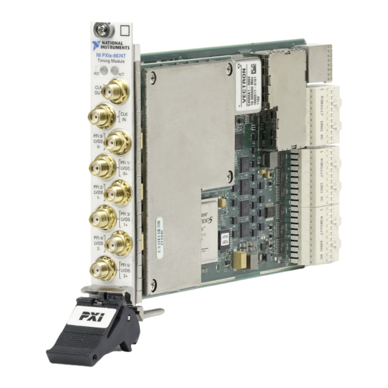
The PXIe-6674T is a PXI Express timing and synchronization module that can generate and route clocks and triggers between devices in a single PXI Express chassis or across multiple PXI and PXI Express chassis. Use the PXIe-6674T to provide advanced triggering schemes, perform synchronization for multiple devices, and improve measurement accuracy for extremely high-channel-count applications. -
Page 5: Components Of A Pxie-6674T System
PXIe-6674T User Manual Components of a PXIe-6674T System The PXIe-6674T is designed for use in a system that includes other hardware components, drivers, and software. Notice A system and the surrounding environment must meet the requirements defined in PXIe-6674T Specifications. - Page 6 PXIe-6674T User Manual Component Description and Recommendations Timing and Synchronization Module The PXIe-6674T timing and Synchronization module. Cables and Accessories Cables and accessories allow connectivity to/ from your instrument for measurements. Refer to Cables and Accessories for recommended cables and accessories and guidance.
- Page 7 G programming language. It features a wide range of analysis functions and interactive, programmable display elements. The LabVIEW Data Acquisition VI Library, a series of virtual instruments for using LabVIEW with National Instruments DAQ hardware, is included with LabVIEW. LabWindows/CVI is a complete ANSI C ADE that features an interactive video interface, code generation tools, and the LabWindows/CVI Data Acquisition and Easy I/O libraries.
-
Page 8: Pxie-6674T Theory Of Operation
■ another. The PXIe-6674T can generate two types of clock signals. The first type of clock signal is generated using the onboard clock generation circuitry based on direct digital synthesis (DDS) with an 800 MHz reference phase locked to PXIe_CLK100. The second type of clock signal is generated with an onboard precision oven controlled crystal oscillator (OCXO). - Page 9 PXIe-6674T User Manual You can use the NI-Sync software or the NI-MAX interface to interact with the PXIe-6674T, including configuring the PFI, PXI_STAR, and PXIe_DSTAR terminals, and specifying the frequencies produced by the DDS clock generation circuitry. Related concepts: Generating and Routing Clocks ■...
- Page 10 PXIe-6674T User Manual Related concepts: Generating and Routing Clocks ■ ni.com...
-
Page 11: Pxie-6674T Front Panel
PXIe-6674T User Manual PXIe-6674T Front Panel Figure 2. PXIe-6674T Front Panel NI PXIe-6674T Timing Module PFI 0/ LVDS PFI 1/ LVDS PFI 2/ LVDS PFI 3/ LVDS PFI 4/ LVDS PFI 5/ LVDS 1. Access LED 2. Active LED 3. SMA Connectors... -
Page 12: Pxie-6674T Pinout
PXIe-6674T User Manual PXIe-6674T Pinout The following figure shows the terminals on the PXIe-6674T front panel. Figure 3. PXIe-6674T Connector Pinout Lorem ipsum CLKOUT CLKIN PFI 0/ LVDS 0- PFI 1/ LVDS 0+ PFI 2/ LVDS 1- PFI 3/ LVDS 1+... - Page 13 Notice Connections that exceed any of the maximum ratings of input or output signals on the PXIe-6674T can damage the module and the computer. NI is not liable for any damage resulting from such signal connections. © National Instruments...
-
Page 14: Pxie-6674T Led Indicators
PXIe-6674T User Manual PXIe-6674T LED Indicators The PXIe-6674T features an Access LED and Active LED. Access LED The Access LED, located on the module front panel, indicates module power and access. The following table lists the Access LED states. Table 5. Access LED... - Page 15 Notice If the Access LED is observed to be solid red, a hardware failure has been detected that may impact the performance of the PXIe-6674T. Contact NI for support. Active LED The Active LED indicates an error or phase-locked loop (PLL) activity. You can change the Active LED to amber, unless an error overrides the selection.
-
Page 16: Pxie-6674T Installation And Configuration
PXIe-6674T User Manual PXIe-6674T Installation and Configuration Complete the following steps to install the PXIe-6674T into a chassis and prepare it for use. Installing the Software Unpacking the Kit Installing the PXIe-6674T into a Chassis Verifying the Installation in MAX Installing the Software You must be an Administrator to install NI software on your computer. -
Page 17: Installing The Pxie-6674T Into A Chassis
Store the device in the antistatic package when the device is not in use. Kit Contents Refer to the following figure to identify the contents of the PXIe-6674T kit. Figure 4. PXIe-6674T Kit Contents 1. PXIe-6674T Module 2. SMA Driver Bit 3. - Page 18 4. Ground yourself using a grounding strap or by touching a grounded object. Make sure you follow the ESD protection precautions. 5. Carefully insert the PXIe-6674T into the system timing slot. Make sure you do not scrape the module on any adjacent modules. Use the injector/ejector handle to fully insert the module into the chassis.
-
Page 19: Verifying The Installation In Max
8. Visually verify the installation. Ensure that the module is fully inserted into the slot. 9. Plug in and power on the chassis. The PXIe-6674T is now installed. Verifying the Installation in MAX Use Measurement & Automation Explorer (MAX) to configure your NI hardware. MAX informs other programs about which NI hardware products are in the system and how they are configured. - Page 20 If error conditions appear, reinstall the NI-Sync driver. What Should I Do if the PXIe-6674T Fails the Self-Test? 1. Reset the PXIe-6674T through MAX, and then perform the self-test again. 2. Restart the system, and then perform the self-test again.
-
Page 21: Pxie-6674T Signal Description
PXIe-6674T User Manual PXIe-6674T Signal Description The following table outlines the function and direction of the signals in the PXIe-6674T. Table 7. PXIe-6674T Signals Signal Name Direction Description PXI_CLK10_IN Out (to chassis) This is a signal that can be used... - Page 22 Out (internal) Clock Generation refers to the clock signal coming from the onboard clock generation circuitry of the PXIe-6674T. The clock generation circuitry can generate a clock from sub-1 Hz to 1 GHz with fine granularity and is automatically locked in phase to PXIe_CLK100.
- Page 23 In/Out (to/from chassis) The PXI trigger bus consists of eight digital lines shared among all slots in the PXI Express chassis. The PXIe-6674T can route a wide variety of signals to and from these lines. Note PXI_TRIG<0..5> are also known as RTSI<0..5>...
- Page 24 PXIe-6674T User Manual Signal Name Direction Description and is capable of high-speed clock distribution. Refer to PXIe DSTARA Network for more information. PXIe_DSTARB Out (to chassis) The PXIe_DSTARB lines connect the system timing module to each peripheral slot in a PXI...
-
Page 25: Generating And Routing Clocks
PXIe-6674T User Manual Generating and Routing Clocks This section describes the two types of clock generation in the PXIe-6674T and explains the considerations for choosing either type. Generating Clocks Using the Onboard Clock Generation Circuitry The PXIe-6674T includes built-in advanced clock generation circuitry for generating clock signals from below 1 Hz to 1 GHz with very fine frequency resolution. -
Page 26: Pxi_Clk10 And Pxie_Clk100
The 800 MHz reference of the DDS clock generation circuitry is phase locked to PXIe_CLK100; therefore, its frequency accuracy is inherited from PXIe_CLK100. To give the best frequency accuracy, the OCXO of the PXIe-6674T can be routed to PXI_CLK10_IN. The chassis can then use the PXI_CLK10_IN to lock PXIe_CLK100 and PXI_CLK10. - Page 27 OCXO to be fine-tuned by varying the control voltage to the OCXO. The PXIe-6674T uses a 16-bit digital analog converter to give precise control of the tuning voltage. While the tuning voltage can be varied by the user, it is normally controlled automatically by software, which sets it to the calibration tuning voltage.
- Page 28 MHz PLL of the PXIe-6674T is able to match the OCXO frequency to the reference clock supplied by the user from CLKIN. Use of the 10 MHz PLL of the PXIe-6674T has advantages over using just CLKIN to drive PXI_CLK10_IN: Reference frequencies other than 10 MHz can be used.
-
Page 29: Pxie_Dstara, Pxie_Dstarb, And Pxie_Dstarc
PXIe_DSTARC uses LVDS signaling and closely matched trace lengths and can be used to send a trigger signal or clock signal to the system timing slot module. The PXIe-6674T receives each PXIe_DSTARC signal and sends a copy to the PXIe_DSTARA network for clock sharing and to the FPGA for trigger routing. - Page 30 PXIe-6674T User Manual Figure 6. PXIe_DSTARA Network PXIe-DSTARA<0..3> CLKIN Bank 0 Fanout PFI_LVDS<0..2> Source A Clock Generation PXIe-DSTARA<4..7> Bank 1 PXIe_DSTARC<0..7> Fanout PXIe-DSTARA<8..11> CLKIN Bank 2 Fanout PFI_LVDS<0..2> Source B Clock Generation PXIe-DSTARA<12..16> To PFI_LVDS 0 Bank 3 To PFI_LVDS 1 PXIe_DSTARC<8..16>...
- Page 31 PXIe-6674T User Manual PFI_LVDS<0..2> To allow for sending and receiving signals between system timing modules that are too fast for single-ended PFI signaling, two PFI SMA connectors can be combined to send or receive LVDS signals. The following table shows the relation between the front panel SMA connectors used for PFI and PFI_LVDS.
- Page 32 The CLKOUT SMA connector on the front panel provides a means to export a clock signal from the PXIe-6674T to an external device or another system timing module. The CLKOUT driver uses two separate circuits for driving CLKOUT, one for low-speed frequencies (50 MHz and below) and one for high-speed frequencies (above 50 MHz).
-
Page 33: Routing Signals
PXIe-6674T User Manual Routing Signals The PXIe-6674T has versatile trigger routing capabilities. It can route signals to and from the front panel, the PXI star triggers, PXIe_DSTARB, and PXIe_DSTARC. Refer to the following figure for the routing features of the PXIe-6674T. -
Page 34: Determining Sources And Destinations
Refer to Choosing the Type of Routing for more information on synchronous versus asynchronous routing. The following figure summarizes the sources and destinations of the PXIe-6674T. The destinations are listed in the horizontal heading row, and the sources are listed in the column at the far left. -
Page 35: Using Front Panel Pfis As Single-Ended Inputs
Note Terminating the signals with a 50 Ω resistance is recommended when the source is another PXIe-6674T or any other source with a 50 Ω output. The voltage thresholds for the front-panel PFI inputs are programmable. The input signal is generated by comparing the input voltage on the PFI connectors to the voltage output of software-programmable DACs. - Page 36 PXIe-6674T User Manual Using Front Panel PFIs as Single-Ended Outputs The front panel PFI outputs are +3.3 V drivers with 50 Ω output impedance. The outputs can drive 50 Ω loads, such as a 50 Ω coaxial cable with a 50 Ω receiver. This cable configuration is the recommended setup to minimize reflections.
-
Page 37: Using Front Panel Pfis For Lvds Triggers
PXIe-6674T User Manual Refer to Choosing the Type of Routing section for more information on the synchronization clock. Note The PFI synchronization clock is the same for all routing operations in which PFI<0..5> or PFI_LVDS<0..2> is defined as the output, although the divide-down ratio for this clock (full rate, first divider, second divider) may be chosen on a per-route basis. -
Page 38: Using The Pxi Triggers
PXIe-6674T User Manual PXIe_CLK100 ■ OCXO ■ CLKIN ■ Any of the previously listed signals divided by the first frequency divider (2 ■ up to 512) Any of the previously listed signals divided by the second frequency divider ■ , up to 512) Refer to the Choosing the Type of Routing section for more information on the synchronization clock. -
Page 39: Using The Pxi Star Triggers
PXIe-6674T User Manual PXI_STAR<0..16> ■ Global software trigger ■ Backplane synchronization clock ■ PXIe_DSTARC ■ Steady logic high or low ■ The backplane synchronization clock may be any of the following signals. Clock Generation ■ PXI_CLK10 ■ PXIe_CLK100 ■ OCXO ■... -
Page 40: Using The Pxie_Dstarb And Pxie_Dstarc Triggers
PXIe-6674T User Manual trigger line be matched to within 1 ns. A typical upper limit for the skew in most NI PXI Express chassis is 500 ps. The low skew of the PXI star trigger bus is useful for applications that require triggers to arrive at several modules nearly simultaneously. -
Page 41: Choosing The Type Of Routing
PXIe_DSTAR routes to 150 ps, thus triggers are sent and received with low skew. The PXIe-6674T can route PXIe_DSTARC inputs to both the PXIe_DSTARA network for use as a clock source and to the FPGA for use as a trigger source. - Page 42 Some delay is always associated with an asynchronous route, and this delay varies among PXIe-6674T modules, depending on variations in temperature and chassis voltage. Typical delay times in the PXIe-6674T for asynchronous routes between various sources and destinations are given in the device's Specifications.
- Page 43 Time, t CtoQ Trigger Output The PXIe-6674T board supports synchronous routing to either the rising or falling edge of the synchronization clock. In addition, the polarity of the destination signal can be inverted, which is useful when handling active-low digital signals.
- Page 44 PXIe-6674T User Manual Figure 12. Synchronous Routing to Multiple Destinations PXI_CLK10 Trigger Out@Source Trigger@Destination 1 Trigger@Destination 2 Trigger Synchronously Received @Destinations 1 and 2 A: Propagation delay from source to destination 1. B: Propagation delay from source to destination 2.
- Page 45 For more information and possible methods to ensure this requirement is met, go to ni.com/ info and enter the Info Code SyncTriggerRouting. Possible sources for synchronous routing with the PXIe-6674T include the following sources: Any front panel PFI pin as single-ended.
- Page 46 OCXO ■ CLKIN ■ One of two "divided copies" of any of the previously listed five signals. ■ The PXIe-6674T includes two clock-divider circuits that can divide the synchronization clock signals by any power of 2 up to 512. ni.com...
-
Page 47: Example Programs
PXIe-6674T User Manual Example Programs NI-Sync includes several example applications that demonstrate the functionality of your device and can serve as interactive tools, programming models, and building blocks for your own applications. NI Example Finder The NI Example Finder is a utility that organizes examples into categories and allows you to browse and search installed examples. - Page 48 Common Example Programs The following example programs in NI Example Finder demonstrate common functions and operations of the PXIe-6674T. • Check Clk10 & Route Clock—Uses the PLL circuit on the CLKIN input to check for the presence of an external clock.
- Page 49 PXIe-6674T User Manual • Route Clock—This example program can either replace the clock on the PXI backplane with a different clock, or it can route a clock from the chassis to the CLK OUT connector. • Route Ground to Trigger (Optional Invert)—Routes a signal (Ground by default) to a specified destination.
-
Page 50: Calibration
PXIe-6674T User Manual Calibration Calibration of the PXIe-6674T consists of verifying the measurement accuracy of the device and correcting for any measurement error. The PXIe-6674T is factory calibrated before shipment at approximately 25 °C to the levels indicated in the PXIe-6674T Specifications. -
Page 51: Cleaning The Pxie-6674T System
PXIe-6674T User Manual Cleaning the PXIe-6674T System NI recommends the following to clean and maintain your instrument's system: Clean the fan filters on the chassis regularly to prevent fan blockage and to ■ ensure efficient air circulation. Cleaning frequency depends on the amount of use and the operating environment.
Need help?
Do you have a question about the PXIe-6674T and is the answer not in the manual?
Questions and answers