Advertisement
Quick Links
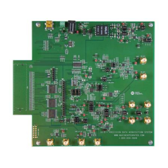
System Board 5944
MAXREFDES74#: 18-BIT PRECISION DATA
ACQUISITION SYSTEM
MAXREFDES74# System Board
Introduction
The MAXREFDES74# reference design performs high-speed, 18-bit, precision data
acquisition based on Maxim's leading-edge, high-accuracy, low-power data converters.
The MAXREFDES74# design works as a building block for a high-speed, low-power,
high-accuracy data acquisition and control system for industrial process control and
automation, and high-speed protection systems for power distribution and automation.
By changing the ADC and DAC to pin-compatible 16-bit devices such as the MAX11166
and the MAX5316, a 16-bit data acquisition system can also be tested.
Advertisement

Related Manuals for Maxim Integrated MAXREFDES Series


Summary of Contents for Maxim Integrated MAXREFDES Series
- Page 1 System Board 5944 MAXREFDES74#: 18-BIT PRECISION DATA ACQUISITION SYSTEM MAXREFDES74# System Board Introduction The MAXREFDES74# reference design performs high-speed, 18-bit, precision data acquisition based on Maxim’s leading-edge, high-accuracy, low-power data converters. The MAXREFDES74# design works as a building block for a high-speed, low-power, high-accuracy data acquisition and control system for industrial process control and automation, and high-speed protection systems for power distribution and automation.
- Page 2 The MAXREFDES74# reference design features: • Power and data isolation • Flexible, configurable inverting or noninverting input scheme • Unipolar or bipolar input (ADC) and output (DAC) MAX11156 • 18-bit resolution with no missing codes • SNR: 94.4dB • THD: -107dB at 1kHz •...
-
Page 3: Detailed Description
• Single 5V supply • True bipolar ±5V input range MAX5318 • 18-bit resolution with no missing codes • High accuracy: ±2 LSB INL (max) • 3µs settling time • User-programmable offset and gain calibration • ±0.5ppm/°C (typ) offset and gain drift over temperature •... -
Page 4: Adc Input Configuration
The voltage reference (V ) for both the ADC and DAC comes from the selectable reference sources, which include the MAX6126, with 3ppm/°C, 0.02% initial accuracy in an 8-pin SO package, and the MAX6070, with 6ppm/°C, 0.04% initial accuracy in a 6-pin SOT23 package. The MAX11156 can use an internal V (default operation) or one of the external references. - Page 5 J10: 1-2 and 9- Noninverting, single-ended, first- CON5: AIN1 J29: 1-2 order LPF or (TP7 and TP15): AIN1 and J32: 3-4 and 7- AGND J10: 1-2 and 9- Differential, first-order LPF CON5 (TP7): AIN1+ J29: Open CON4 (TP10): AIN1- J32: 3-4 and 7- J10: 1-2 and 9- Inverting, single-ended, first- CON4: AIN1 or (TP10 and...
- Page 6 Table 2. DAC Output Configuration CONFIG DAC OUTPUT SHUNT OUTPUT CONNECTORS POSITIONS Single ended, 0 to 3 x V J9: 1-2 CON11: DAC_OUT+ J5: 1-2 or (TP46 and TP41): J18: 1-2 DAC_OUT+ and AGND Single ended, 0 to -3 x V J9: 1-2 CON10: DAC_OUT- J5: 1-2...
-
Page 7: Power Supply
Figure 2. Default shunt positions. Power Supply The MAXREFDES74# board receives power from a single DC source of 15V to 20V, 300mA through a J1 power jack. The MAX13256, H-bridge driver and transformer create an additional negative rail for +20V and -20V. The power is then rectified and regulated down to a +15V and -15V supplies for the op amps, as well as into +5V and 3.3V V for V... - Page 8 Table 4. Power Supply to the Board POWER INPUT SHUNT CONNECTORS POSITIONS Single +15V to +20V input from a wall adapter J30: 1-2 Enable U1 (default) J15: 3-4 J16: 3-4 J17: 3-4 J24: 5-6 An external ±20V TP35 (+20V) J30: 2-3 Disable TP30 (-20V) TP36 (Common 0V) J15: 1-2...
- Page 9 Procedure The MAXREFDES74# board is fully assembled and tested. Follow the steps below to verify board operation: 1. Download the latest version of the MAXREFDES74# Software MAXREFDES74# Zedboard firmware. Save the firmware and software to a temporary folder and uncompress the zip files. Store the firmware file to an SD card. 2.
- Page 10 Figure 3. MAXREFDES74# GUI. 13. Verify the Clock Source, Sampling Rate, Number of Samples, and Configuration of the MAX11156 ADC, and click the Set button. 14. Go to the DMM tab, select mV from the Display Units pulldown menu and click the Capture button.
- Page 11 Figure 5. Scope tab. Figure 6. Histogram tab. Figure 7. FFT tab.
- Page 12 16. Place a J26 shunt and repeat the performance of the V /2 reading. 17. Apply a 10kHz sine wave from an external source, e.g. Audio Precision 2700, to CON3 (AIN0+). Synchronize the external source with the MAXREFDES74# ADC by connecting CON9 (SYNC_CLK_OUT) to the REF IN input for coherent sampling.
- Page 13 Also see: Bipolar Work Around for the MAXREFDES74 › All Design Files Download All Design Files Hardware Files: Schematic Bill of Materials (BOM) PCB Layout PCB Gerber Software Files: Software GUI Firmware Files: ZedBoard Firmware Part Number MAXREFDES74# Active Status Carrier Type https://www.maximintegrated.com/en/design/reference-design-center/system-board/5944.html/tb_tab0/6-20-19...
Need help?
Do you have a question about the MAXREFDES Series and is the answer not in the manual?
Questions and answers