Table of Contents
Advertisement
Quick Links
WWW.INFOPULSAS.LT / info@infopulsas.lt
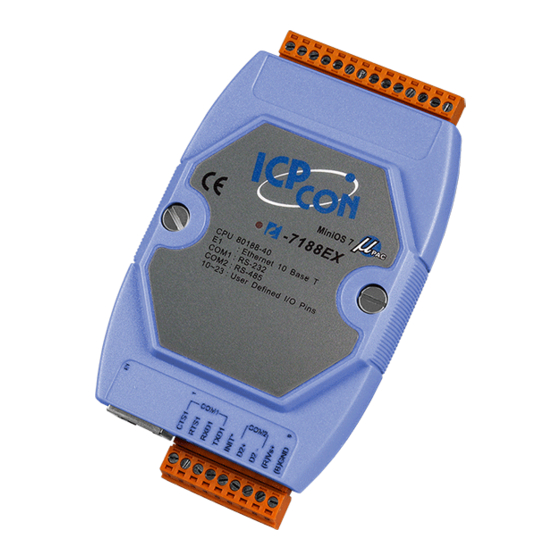
I/O Expansion Bus for 7188X/7188E
User's Manual
Warranty
All products manufactured by ICP DAS are warranted against
defective materials for a period of one year from the date of
delivery to the original purchaser.
Warning
ICP DAS assume no liability for damages consequent to the
use of this product. ICP DAS reserves the right to change this
manual at any time without notice. The information furnished
by ICP DAS is believed to be accurate and reliable. However,
no responsibility is assumed by ICP DAS for its use, not for
any infringements of patents or other rights of third parties
resulting from its use.
Copyright
Copyright 2002 by ICP DAS. All rights are reserved.
Trademark
The names used for identification only may be registered
trademarks of their respective companies.
I/O Expansion Bus for 7188X/7188E User's Manual, Jan/2005 v1.5, 7PH-000-15---1
Advertisement
Table of Contents

Related Manuals for ICP DAS USA 7188X


Summary of Contents for ICP DAS USA 7188X
- Page 1 Copyright Copyright 2002 by ICP DAS. All rights are reserved. Trademark The names used for identification only may be registered trademarks of their respective companies. I/O Expansion Bus for 7188X/7188E User’s Manual, Jan/2005 v1.5, 7PH-000-15---1...
-
Page 2: Table Of Contents
XPANSION OARD FOR I/O E SRAM, F ..........34 XPANSION OARD FOR LASH X0XX I/O EXPANSION BOARDS..............35 X000 :P ............... 35 ROTOTYPE OARD X001: P ............... 36 ROTOTYPE OARD I/O Expansion Bus for 7188X/7188E User’s Manual, Jan/2005 v1.5, 7PH-000-15---2... - Page 3 X308: AD*4 + DO*6 ................84 10.10 X310: AD*2 + DA*2 + DO*3 + DI*3 ............86 X4XX I/O EXPANSION BOARDS ............. 88 11.1 X400:T *3 ................. 88 IMER COUNTER I/O Expansion Bus for 7188X/7188E User’s Manual, Jan/2005 v1.5, 7PH-000-15---3...
- Page 4 12.14 X560: RS-232 * 3 + 8 M F ............111 LASH X6XX I/O EXPANSION BOARDS ............113 13.1 X600 X601 : F ROM............... 113 LASH 13.2 X607 X608: SRAM ................ 114 I/O Expansion Bus for 7188X/7188E User’s Manual, Jan/2005 v1.5, 7PH-000-15---4...
-
Page 5: Introduction
Special software requirement applications Combine special hardware & software applications So we developed an I/O expansion bus in the 7188X / 752N / 7188E family to solve all these applications above. The I/O expansion bus can be used to implement various I/O functions such as D/I, D/O, A/D, D/A, Timer/Counter, UART, I/O Expansion Bus for 7188X/7188E User’s Manual, Jan/2005 v1.5, 7PH-000-15---5... - Page 6 550 mA@5V So I/O=550-280=270 mA max. Note:The 7188XA(D) supports I/O expansion bus but does not support user defined pins, so the 7188XA only supports X002, X003, X560, X600, X601, X607, X608. I/O Expansion Bus for 7188X/7188E User’s Manual, Jan/2005 v1.5, 7PH-000-15---6...
- Page 7 After the above steps, user can combine the standard-7000 modules & customized-7000 modules to solve all applications in the same RS-485 network. This customized solution diagram is given as follows: I/O Expansion Bus for 7188X/7188E User’s Manual, Jan/2005 v1.5, 7PH-000-15---7...
- Page 8 & software Time-to-market solution user’s special requirements (any high speed, complex or combined functions of D/I/O, A/D, D/A, ….., etc.) Robust, stable, flexible, time-to-market & cost-effective total solution. I/O Expansion Bus for 7188X/7188E User’s Manual, Jan/2005 v1.5, 7PH-000-15---8...
-
Page 9: Reconfiguring The 7188Xc(D)/7521(D)
If the DO2 is reconfigured to D/I, its initial state must be High. If its initial state is LOW, system clock will be reduced to 10M. So all clock-related libraries will only be at half-speed. Refer to next page for more information. I/O Expansion Bus for 7188X/7188E User’s Manual, Jan/2005 v1.5, 7PH-000-15---9... - Page 10 The I-7188XB(D), I-7188XG(D), I-7188EX(D), I-7188EG(D) has 14 user-defined pins. But the I-7188XB(D), I-7188XG(D), I-7188EX(D),I- 7188EG(D) & I-7188XA(D) don’t support the reconfiguration-resistor. So the user-defined pins of the 7188X / 7521 family are given as follows: Module User defined pins...
- Page 11 Serial number= 5A 5A 5A 5A 5A 5A 5A 5A 7188x> To burn an ISaGRAF embedded driver, follow the following steps. 8. Copy the program of the correct version into your "7188X" folder. For example, version 1.25, copy \Napdos\Appication\application 11\english\7188xc\PWM.exe to C:\7188X\PWM.exe...
- Page 12 1) autoexec.bat 04/13/2001 16:50:27 20[00014]9039:000C-903B:0000 Total File number is 2 Free space=392240 bytes 14. Press ALT_X to exit "7188x". 15. Remove the connection between "INIT" - "INIT COM", reset the I-7188XC controller. I/O Expansion Bus for 7188X/7188E User’s Manual, Jan/2005 v1.5, 7PH-000-15---12...
-
Page 13: Reference Guide
X series for I-7188EX ftp://ftp.icpdas.com/pub/cd/8000cd/napdos/7188e/minios7/demo/bc/ioexpbus/ X series for I-7188XG ( English_manu, Driver, Demo ) ftp://ftp.icpdas.com/pub/cd/8000cd/napdos/isagraf/7188xg/ X series for I-7188EG ( English_manu, Driver, Demo ) ftp://ftp.icpdas.com/pub/cd/8000cd/napdos/isagraf/7188eg/ 2.2.3 Performance: CD \Napdos\7188x\manual\hardware\x-Performance ftp://ftp.icpdas.com/pub/cd/8000cd/napdos/7188x/manual/hardware/x-performance/ I/O Expansion Bus for 7188X/7188E User’s Manual, Jan/2005 v1.5, 7PH-000-15---13... -
Page 14: Wire Connection
DI value as Relay Contact TTL/CMOS Logic Open Collector 3.2 Digital Output Wire Connection : ON State OFF State Output Type DO value as DO value as Drive Relay Resistance Load I/O Expansion Bus for 7188X/7188E User’s Manual, Jan/2005 v1.5, 7PH-000-15---14... -
Page 15: Voltage Input Wire Connection
Voltage Input Wire Connection: Input Type Voltage Output Wire Connection: Output Type Current Input Wire Connection: Input Type I/O Expansion Bus for 7188X/7188E User’s Manual, Jan/2005 v1.5, 7PH-000-15---15... -
Page 16: Mounting Of I/O Expansion Bus
4. Mounting of I/O Expansion Bus 4.1 Minimal mounting with 7-segmemt display Before mounting: X000 After mounting: I/O Expansion Bus for 7188X/7188E User’s Manual, Jan/2005 v1.5, 7PH-000-15---16... -
Page 17: Medium Mounting Without 7-Seg Display
Medium mounting without 7-SEG display Before mounting: X001 After mounting: I/O Expansion Bus for 7188X/7188E User’s Manual, Jan/2005 v1.5, 7PH-000-15---17... -
Page 18: Mounting Without Case
Mounting without CASE Before mounting: X002 After mounting: I/O Expansion Bus for 7188X/7188E User’s Manual, Jan/2005 v1.5, 7PH-000-15---18... -
Page 19: Odm Mounting Without Case
4.4 ODM mounting without CASE Before mounting: X002 After mounting: I/O Expansion Bus for 7188X/7188E User’s Manual, Jan/2005 v1.5, 7PH-000-15---19... -
Page 20: I/O Expansion Bus
I/O Expansion Bus The I/O expansion bus of 7188X/7188E series can be divided into 3 groups as follows: 1. Power supply & reset signals: VCC, GND, RESET, /RESET 2. Parallel Bus: System clock: CLOCKA Asynchronous ready control: ARDY Address bus: A0 ~ A6, A7 (7188XC & 7521 series without Data bus: D0 ~ D7 Interrupt control: INT0, INT1, INT4 (7188XC &... -
Page 21: Definition
Timer input 1 of CPU (can be used as programmable D/I/O) SCLK Common serial clock output of 7188 series DIO9 Programmable D/I/O bit DIO4 Programmable D/I/O bit DIO14 Programmable D/I/O bit Power supply of PCB Power supply of PCB I/O Expansion Bus for 7188X/7188E User’s Manual, Jan/2005 v1.5, 7PH-000-15---21... - Page 22 TI_0, TI_1: can be used as CPU’s timer input or programmable D/I/O DIO4, DIO9, DIO14: programmable D/I/O bit SCLK: the 7188X/7188E series use this signal as a CLOCK source to drive all on-board serial devices, so it is always be programmed as D/O. Change this signal to other configuration will cause serious errors.
- Page 23 & must be N/C for 7188XC & 752N series Write strobe output (synchronous, active low) Chip select output (synchronous, active low) Read strobe output (synchronous, active low) I/O Expansion Bus for 7188X/7188E User’s Manual, Jan/2005 v1.5, 7PH-000-15---23...
- Page 24 The CS\ will be active if program input/output from I/O address 0 to 0xff. The pin_15 & pin_17 are reserved by 7188XC & 7521 series; user must left these two pins N/C for 7188XC & 7521 series. I/O Expansion Bus for 7188X/7188E User’s Manual, Jan/2005 v1.5, 7PH-000-15---24...
-
Page 25: Parallel Bus
CLKOUTA A12-A0 Address D7-D0 Data (Read) D7-D0 (Write) Data Case 1 Case 2 Case 3 Case 4 Address Data Phase Phase CLKOUTA ARDY (Normally Not-Ready System) ARDY (Normally Ready System) I/O Expansion Bus for 7188X/7188E User’s Manual, Jan/2005 v1.5, 7PH-000-15---25... - Page 26 Read DI 8 to 15 DI_8_15=inportb (BASE+1); The power-up default value of BASE is 0. It is not recommended to change the value of BASE from 0 to another value. I/O Expansion Bus for 7188X/7188E User’s Manual, Jan/2005 v1.5, 7PH-000-15---26...
- Page 27 Write value_2 to DO 8 to 15 outportb (BASE+1, value_2); The power-up default value of BASE is 0. It is not recommended to change the value of BASE from 0 to another value. I/O Expansion Bus for 7188X/7188E User’s Manual, Jan/2005 v1.5, 7PH-000-15---27...
- Page 28 Timer/Counter_1 BASE+1 Timer/Counter_2 BASE+2 Control word BASE+3 The power-up default value of BASE is 0. It is not recommended to change the value of BASE from 0 to another value. I/O Expansion Bus for 7188X/7188E User’s Manual, Jan/2005 v1.5, 7PH-000-15---28...
- Page 29 The power-up default value of BASE is 0. It is not recommended to change the value of BASE from 0 to another value. Note: it is compatible to COM3 of 7188XC/7188XB/7188E library. I/O Expansion Bus for 7188X/7188E User’s Manual, Jan/2005 v1.5, 7PH-000-15---29...
-
Page 30: Serial Bus
/* set the D/O_4 ON or OFF */ if(data) /* set D/O_4 ON */ outport(0Xff74, mport(0Xff74)|(1<<4)); else /* set D/O_4 OFF */ outport(0Xff74, mport(0Xff74)&~(1<<4)); GetDio4(void) /* read the status of D/I_4 */ return mport(0Xff74)&0x0010;} I/O Expansion Bus for 7188X/7188E User’s Manual, Jan/2005 v1.5, 7PH-000-15---30... - Page 31 User can use this signal to drive external serial devices without any side effects. The software driver provides two subroutine to set SCLK high or low as follows: ClockLow(); /* SCLK=0=Low */ ClockHigh(); /* SCLK=1=High */ I/O Expansion Bus for 7188X/7188E User’s Manual, Jan/2005 v1.5, 7PH-000-15---31...
-
Page 32: Selection Guide
XB / XG / EX / EG X110 XB / XG / EX / EG X111 XB / XG / EX / EG 3 channels X400 Timer/Counter 16-bit timer/ counter I/O Expansion Bus for 7188X/7188E User’s Manual, Jan/2005 v1.5, 7PH-000-15---32... -
Page 33: I/O Expansion Board For A/D, D/A, Di, Do
X505 RS-232 Three channels ( 5-wire ) 115.2K XB / XG / EX / EG X506 RS-232 Six channels ( 3-wire ) 115.2K XB / XG / EX / EG I/O Expansion Bus for 7188X/7188E User’s Manual, Jan/2005 v1.5, 7PH-000-15---33... -
Page 34: I/O Expansion Board For Sram, Flash
XA / XC / XB / XG / EX / EG SRAM board Battery backup X608 512 K bytes XA / XC / XB / XG / EX / EG SRAM board I/O Expansion Bus for 7188X/7188E User’s Manual, Jan/2005 v1.5, 7PH-000-15---34... -
Page 35: X0Xx I/O Expansion Boards
CON5 CON5 SIP5/2.0 SIP5/2.0 FEMALE FEMALE CON13 CON5 CON5 CON5 SIP5/2.0 SIP5/2.0 SIP5/2.0 MALE MALE MALE On Board : JP8 , JP9 (close) Daughter Board : JP9 , JP10 (close) I/O Expansion Bus for 7188X/7188E User’s Manual, Jan/2005 v1.5, 7PH-000-15---35... -
Page 36: X001: Prototype Board
<1ST PART FIELD> FEMALE FEMALE CON5 CON5 SIP5/2.0 SIP5/2.0 FEMALE FEMALE LED2 CON13 CON3 <1ST PART FIELD> FEMALE CON5 CON5 CON5 LED_DI SIP5/2.0 SIP5/2.0 SIP5/2.0 MALE LED_LOAD MALE MALE LED_SCLK I/O Expansion Bus for 7188X/7188E User’s Manual, Jan/2005 v1.5, 7PH-000-15---36... -
Page 37: X002 : Prototype Board
ARDY INTO INT1 RESET\ RESET RESET\ BCS\ TO_0 TO_ 1 BWR\ 74LS273 TI_ 0 TI _1 BRD\ SCLK DIO9 DIO4 DIO14 VCC=20 Gnd=10 CON20A MALE 74LS245 0.1u VCC=20 0.1u Gnd=10 I/O Expansion Bus for 7188X/7188E User’s Manual, Jan/2005 v1.5, 7PH-000-15---37... -
Page 38: X003: Test Board 1
DI1 to DO1, DI2 to DO2, DI3 to DO3. When you want to test DI and DO of I-7188XA (D) or I-7521, Please connect DI1 to DO1, DI2 to DO2. I/O Expansion Bus for 7188X/7188E User’s Manual, Jan/2005 v1.5, 7PH-000-15---38... -
Page 39: X004: T B 2
S_CLK --> DIO9 OK!!! DIO4 --> DIO14 OK!!! DIO4 <-- DIO14 OK!!! Data Bus Test OK! Test Timer 0 10 Timer0/INT0 Test OK Test Timer 1 10(00000) Timer1/INT1 Test OK I/O Expansion Bus for 7188X/7188E User’s Manual, Jan/2005 v1.5, 7PH-000-15---39... - Page 40 S_CLK --> DIO9 OK!!! DIO4 --> DIO14 OK!!! DIO4 <-- DIO14 OK!!! Data Bus Test OK! Test Timer 0 10 Timer0/INT0 Test OK Test Timer 1 10(00000) Timer1/INT1 Test OK I/O Expansion Bus for 7188X/7188E User’s Manual, Jan/2005 v1.5, 7PH-000-15---40...
- Page 41 S_CLK --> DIO9 OK!!! DIO4 --> DIO14 OK!!! DIO4 <-- DIO14 OK!!! Data Bus Test OK! Test Timer 0 10 Timer0/INT0 Test OK Test Timer 1 10(00000) Timer1/INT1 Test OK I/O Expansion Bus for 7188X/7188E User’s Manual, Jan/2005 v1.5, 7PH-000-15---41...
-
Page 42: X1Xx I/O Expansion Boards
Input Range / Type : Logic high level (3.5V~30V), Logic low level (0V~1V) Isolated : none. 8.1.2 Pin Assignment: (X100) COM2 Note: refer to section 3. for A/D, D/A, DI, DO wire connection. I/O Expansion Bus for 7188X/7188E User’s Manual, Jan/2005 v1.5, 7PH-000-15---42... - Page 43 2. It is not recommended to change the value of BASE from 0 to another value. 3. DiVal=0 all 8-channel are Low DiVal=1 Chennel_0 is High, the other channels are Low DiVal=0xff all 8-channel are High I/O Expansion Bus for 7188X/7188E User’s Manual, Jan/2005 v1.5, 7PH-000-15---43...
-
Page 44: X101: Do * 8
High Voltage : 2.4V (Min) Low Voltage : 0.8 (Max) Sink current: 64mA (Max) Isolated: none. 8.2.2 Pin Assignment: (X101) COM2 Note: refer to section 3. for A/D, D/A, DI, DO wire connection. I/O Expansion Bus for 7188X/7188E User’s Manual, Jan/2005 v1.5, 7PH-000-15---44... - Page 45 2. It is not recommended to change the value of BASE from 0 to another value. 3. DoVal=0 turn all 8-channel OFF DoVal=1 turn chennel_0 ON, the other channels OFF DoVal=0xff turn all 8-channel ON I/O Expansion Bus for 7188X/7188E User’s Manual, Jan/2005 v1.5, 7PH-000-15---45...
-
Page 46: X102: Relay * 2
Relay on time (typical) : 6ms • Relay off time (typical) : 6ms 8.3.2 Pin Assignment: (X102) COM2 NO ( Normal Open ) O.C. NC ( Normal Close ) Relay COM ( Common ) I/O Expansion Bus for 7188X/7188E User’s Manual, Jan/2005 v1.5, 7PH-000-15---46... - Page 47 SetDio14Dir( 0 ); // Set channel-1 to DO SetDio4Low(); // Turn channel_0 relay OFF SetDio14Low(); // Turn channel_1 relay OFF SetDio4High(); // Turn channel_0 relay ON SetDio14High(); // Turn channel_1 relay ON I/O Expansion Bus for 7188X/7188E User’s Manual, Jan/2005 v1.5, 7PH-000-15---47...
-
Page 48: X103: Isolated Di * 7
Input Range / Type : Logic high level (3.5V~30V), Logic low level (0V~1V) Isolated digital input. 8.4.2 Pin Assignment: (X103) COM2 Note: refer to section 3. for A/D, D/A, DI, DO wire connection. I/O Expansion Bus for 7188X/7188E User’s Manual, Jan/2005 v1.5, 7PH-000-15---48... - Page 49 SetDio4Dir(1); XDI5=GetDio4(); // set to D/I & read D/I, channel_5 SetTi0Dir(1); XDI6=GetTi0(); // set to D/I & read D/I, channel_6 SetTo0Dir(1); XDI7=GetTo0(); // set to D/I & read D/I, channel_7 I/O Expansion Bus for 7188X/7188E User’s Manual, Jan/2005 v1.5, 7PH-000-15---49...
-
Page 50: X104: D/I/O * 8, Single-Bit
Input / Output: each channel can be programmed to D/I or D/O. Input Range: 0~5V(Max) Isolated: none. 8.5.2 Pin Assignment: (X104) COM2 Note: Provide functions of DI and DO from CPU. I/O Expansion Bus for 7188X/7188E User’s Manual, Jan/2005 v1.5, 7PH-000-15---50... - Page 51 Programming: Software library void SetDio4Dir(int dir); void SetDio4High(void); void SetDio4Low(void); int GetDio4(void); void SetDio9Dir(int dir); void SetDio9High(void); void SetDio9Low(void); int GetDio9(void); void SetDio14Dir(int dir); void SetDio14High(void); void SetDio14Low(void); int GetDio14(void); I/O Expansion Bus for 7188X/7188E User’s Manual, Jan/2005 v1.5, 7PH-000-15---51...
- Page 52 GetTo0(void); void SetDo1High(void); void SetDo1Low(void); int GetDo1(void); void SetDo2High(void); void SetDo2Low(void); int GetDo2(void); void SetDo3High(void); void SetDo3Low(void); int GetDo3(void); int GetDi2(void); int GetDi3(void); void ClockHighLow(void); void ClockHigh(void); void ClockLow(void); I/O Expansion Bus for 7188X/7188E User’s Manual, Jan/2005 v1.5, 7PH-000-15---52...
-
Page 53: X105: D/I/O * 8, 8-Bit
Logic low level (0V~1V) Isolated: none Digital Output: Channels: 8 Output: TTL level Isolated: none 8.6.2 Pin Assignment: (X105) COM2 Note: refer to section 3. for A/D, D/A, DI, DO wire connection. I/O Expansion Bus for 7188X/7188E User’s Manual, Jan/2005 v1.5, 7PH-000-15---53... - Page 54 ON, the other channels OFF DoVal=0xFF turn all 8-channel ON DIO14 is used to select D/I or D/O If DIO14 is LOW select D/O*8 D/I is read-back value of D/O I/O Expansion Bus for 7188X/7188E User’s Manual, Jan/2005 v1.5, 7PH-000-15---54...
- Page 55 /* read D/I*8 (from J5) Select D/I*8 as following: SetDio14Dir(0); /* select DIO14 as D/O SetDio14Low(); /* select D/O*8 outportb(BASE,DoVal); /* set value of D/O*8 (to J5) DiVal=inportb(BASE); /* D/O*8 read back I/O Expansion Bus for 7188X/7188E User’s Manual, Jan/2005 v1.5, 7PH-000-15---55...
-
Page 56: X106: Do *2 Or Di *3
Isolated: none Digital Output: Channels:3 Open-collector Output: 250 mA / 30V max Isolated: none 8.7.2 Pin Assignment: (X106) COM2 Note: refer to section 3. for A/D, D/A, DI, DO wire connection. I/O Expansion Bus for 7188X/7188E User’s Manual, Jan/2005 v1.5, 7PH-000-15---56... - Page 57 Data = SetDio9Dir( 1 ); // Set D/I channel_3 Data = GetTo1Dir( ); // Read D/I channel_1 Data = GetTo0Dir( ); // Read D/I channel_2 Data = GetDio9Dir( ); // Read D/I channel_3 I/O Expansion Bus for 7188X/7188E User’s Manual, Jan/2005 v1.5, 7PH-000-15---57...
-
Page 58: X107: Di * 6 And Do * 7
Digital Output: Channels: 7 Open-collector Output: 100 mA / 30V max Isolated: none 8.8.2 Pin Assignment : (X107) Note: refer to section 3. for A/D, D/A, DI, DO wire connection. I/O Expansion Bus for 7188X/7188E User’s Manual, Jan/2005 v1.5, 7PH-000-15---58... - Page 59 2. It is not recommended to change the value of BASE from 0 to another value. 3. DoVal=0x00 turn all 7-channel OFF DoVal=0x01 turn chennel_0 ON, the other channels OFF DoVal=0x7F turn all 7-channel ON I/O Expansion Bus for 7188X/7188E User’s Manual, Jan/2005 v1.5, 7PH-000-15---59...
-
Page 60: X108: Pwm * 2
8.9 X10⁸: PWM * 2 8.9.1 Specifications: I-7188XC Power consumption: 0.5 W Frequency : Low frequency : 40Hz High frequency : 100KHz Open-collector output: 250mA/30V, Max (Per channel) 8.9.2 Pin Assignment: (X108) COM2 I/O Expansion Bus for 7188X/7188E User’s Manual, Jan/2005 v1.5, 7PH-000-15---60... - Page 61 --> !01 100 1 1 1 #01A1 200 2 1 --> !01 chan_1 200 2 1 #01C1 --> !01 200 2 1 1 #01B10 --> !01 chan_1 Off #01C1 --> !01 200 2 1 0 I/O Expansion Bus for 7188X/7188E User’s Manual, Jan/2005 v1.5, 7PH-000-15---61...
- Page 62 #01B00 --> !01 CHAN_0 Off #01C0 --> !01 100 1 1 0 5. Run Visual Basic: I/O Expansion Bus for 7188X/7188E User’s Manual, Jan/2005 v1.5, 7PH-000-15---62...
-
Page 63: X109: Photo Mos Relay * 7
2. It is not recommended to change the value of BASE from 0 to another value. 3. DoVal=0x00 turn all 7-channel OFF DoVal=0x01 turn chennel_0 ON, the other channels OFF DoVal=0x7F turn all 7-channel ON I/O Expansion Bus for 7188X/7188E User’s Manual, Jan/2005 v1.5, 7PH-000-15---63... -
Page 64: X110: 14 Channels D/I
8.11.3 Programming : iValue = inpw(port); /* for all 14-channel */ DiVal=0x0000 all 14-channel are Low DiVal=0x0001 Chennel_0 is High, the other channels are Low DiVal=0x3FFF all 14-channel are High I/O Expansion Bus for 7188X/7188E User’s Manual, Jan/2005 v1.5, 7PH-000-15---64... -
Page 65: X111: 13 Channels D/O
/* for all 13-channels */ Please notice that Base address “0x0080” not used. DoVal=0x0000 turn all 13-channel OFF DoVal=0x0001 turn chennel_0 ON, the other channels OFF DoVal=0x2000 turn all 13-channel ON I/O Expansion Bus for 7188X/7188E User’s Manual, Jan/2005 v1.5, 7PH-000-15---65... -
Page 66: X2Xx I/O Expansion Boards
Pin Assignment : (X200) COM2 Note: refer to section 3. for A/D, D/A, DI, DO wire connection. 9.1.3 Programming : For Software Installation & Demo Program, Refer to Section 2.2.2 I/O Expansion Bus for 7188X/7188E User’s Manual, Jan/2005 v1.5, 7PH-000-15---66... -
Page 67: X201: Ad*4
Input Range/Type : 0 ~ 20mA Sampling rate : 900 Hz Isolated : none 9.2.2 Pin Assignment : (X201) COM2 Note: refer to section 3. for A/D, D/A, DI, DO wire connection. I/O Expansion Bus for 7188X/7188E User’s Manual, Jan/2005 v1.5, 7PH-000-15---67... - Page 68 Five channels of isolated DI Jumper: Select TP0 or TP1 function TP0: JP9 and JP8 closed TP1: JP9 and JP10 closed 9.2.4 Programming : For Software Installation & Demo Program, Refer to Section 2.2.2 I/O Expansion Bus for 7188X/7188E User’s Manual, Jan/2005 v1.5, 7PH-000-15---68...
-
Page 69: X202: Ad*7
9.3.2 Pin Assignment : (X202) Note: refer to section 3. for A/D, D/A, DI, DO wire connection. 9.3.3 Programming : For Software Installation & Demo Program, Refer to Section 2.2.2 I/O Expansion Bus for 7188X/7188E User’s Manual, Jan/2005 v1.5, 7PH-000-15---69... -
Page 70: X203: Ad*2 + Do*6 + Di*2
Open-collector Output: 100 mA / 30V max Isolated: none 9.4.2 Pin Assignment : (X203) Note: Refer to section 3. for A/D, D/A, DI, DO wire connection. For Software Installation & Demo Program, Refer to Section 2.2.2 I/O Expansion Bus for 7188X/7188E User’s Manual, Jan/2005 v1.5, 7PH-000-15---70... -
Page 71: X3Xx I/O Expansion Boards
Pin Assignment : (X300) COM2 Note: refer to section 3. for A/D, D/A, DI, DO wire connection. 10.1.3 Programming : For Software Installation & Demo Program, Refer to Section 2.2.2 I/O Expansion Bus for 7188X/7188E User’s Manual, Jan/2005 v1.5, 7PH-000-15---71... -
Page 72: X301: Da * 1 + Ad * 1
Input Range/Type : 0 ~ 2.5V Sampling rate : 900 Hz Isolated : none 10.2.2 Pin Assignment : (X301) COM2 Note: refer to section 3. for A/D, D/A, DI, DO wire connection. I/O Expansion Bus for 7188X/7188E User’s Manual, Jan/2005 v1.5, 7PH-000-15---72... - Page 73 DataIn = 0 – 4095 (Note 4095 4.095V) int AnalogIn( void ) Return value= 0 - 4095 Mapping formula: Vref / 4096 (Note: Vref=2.5v) For Software Installation & Demo Program, Refer to Section 2.2.2 I/O Expansion Bus for 7188X/7188E User’s Manual, Jan/2005 v1.5, 7PH-000-15---73...
-
Page 74: X302: Da * 1 + Ad * 1
Input Range/Type : +/- 5V Sampling rate : 900 Hz Isolated : none 10.3.2 Pin Assignment : (X302) COM2 Note: refer to section 3. for A/D, D/A, DI, DO wire connection. I/O Expansion Bus for 7188X/7188E User’s Manual, Jan/2005 v1.5, 7PH-000-15---74... - Page 75 Maximum: +/- 2 LSB (+- 4.8 mV) [D/A] thoughput : 1300 data/sec (with floating convertion) Accuracy==> Typical: +/- 1 LSB (+- 2.4 mV) Maximum: +/- 2 LSB (+- 4.8 mV) I/O Expansion Bus for 7188X/7188E User’s Manual, Jan/2005 v1.5, 7PH-000-15---75...
-
Page 76: X303: Ad*1 + Da*1 + Do*6 + Di*4
Digital Input : Channels: 4 Input Range / Type: Logic high level (3.5V~30V), Logic low level (0V~1V) Isolated: none Digital Output: Channels: 6 Open-collector Output: 100 mA / 30V max Isolated: none I/O Expansion Bus for 7188X/7188E User’s Manual, Jan/2005 v1.5, 7PH-000-15---76... - Page 77 : 1300 data/sec (with floating convertion) Accuracy==> Typical: +/- 1 LSB (+- 2.4 mV) Maximum: +/- 2 LSB (+- 4.8 mV) [D/O] throughput: can generates 2KHz square wave signals. I/O Expansion Bus for 7188X/7188E User’s Manual, Jan/2005 v1.5, 7PH-000-15---77...
-
Page 78: X304: Ad*3 + Da*1 + Do*4 + Di*4
Digital Input : Channels: 4 Input Range / Type: Logic high level (3.5V~30V), Logic low level (0V~1V) Isolated: none Digital Output: Channels: 4 Open-collector Output: 100 mA / 30V max Isolated: none I/O Expansion Bus for 7188X/7188E User’s Manual, Jan/2005 v1.5, 7PH-000-15---78... - Page 79 : 1300 data/sec (with floating convertion) Accuracy==> Typical: +/- 1 LSB (+- 2.4 mV) Maximum: +/- 2 LSB (+- 4.8 mV) [D/O] throughput: can generates 2KHz square wave signals. I/O Expansion Bus for 7188X/7188E User’s Manual, Jan/2005 v1.5, 7PH-000-15---79...
-
Page 80: X305: Ad*7 + Da*1 + Do*2 + Di*2
Digital Input : Channels: 2 Input Range / Type: Logic high level (3.5V~30V), Logic low level (0V~1V) Isolated: none Digital Output: Channels: 2 Open-collector Output: 100 mA / 30V max Isolated: none I/O Expansion Bus for 7188X/7188E User’s Manual, Jan/2005 v1.5, 7PH-000-15---80... - Page 81 : 1300 data/sec (with floating convertion) Accuracy==> Typical: +/- 1 LSB (+- 2.4 mV) Maximum: +/- 2 LSB (+- 4.8 mV) [D/O] throughput: can generates 2KHz square wave signals. I/O Expansion Bus for 7188X/7188E User’s Manual, Jan/2005 v1.5, 7PH-000-15---81...
-
Page 82: X306: Ad*2
Pin Assignment : (X306) COM2 Note: refer to section 3. for A/D, D/A, DI, DO wire connection. Programming : 10.7.3 For Software Installation & Demo Program, Refer to Section 2.2.2 I/O Expansion Bus for 7188X/7188E User’s Manual, Jan/2005 v1.5, 7PH-000-15---82... -
Page 83: X307: Ad*8
10.8.2 Pin Assignment : (X307) Note: refer to section 3. for A/D, D/A, DI, DO wire connection. 10.8.3 Programming : For Software Installation & Demo Program, Refer to Section 2.2.2 I/O Expansion Bus for 7188X/7188E User’s Manual, Jan/2005 v1.5, 7PH-000-15---83... -
Page 84: X308: Ad*4 + Do*6
Digital Output: Channels: 6 Open-collector Output: 100 mA / 30V max Isolated: none 10.9.2 Pin Assignment : (X308) Note: Refer to section 3. for A/D, D/A, DI, DO wire connection. I/O Expansion Bus for 7188X/7188E User’s Manual, Jan/2005 v1.5, 7PH-000-15---84... - Page 85 1800 data/sec (with floating convertion) Accuracy==> Typical: +/- 1 LSB (+- 2.4 mV) Maximum: +/- 2 LSB (+- 4.8 mV) [D/O] throughput: can generates 2KHz square wave signals. I/O Expansion Bus for 7188X/7188E User’s Manual, Jan/2005 v1.5, 7PH-000-15---85...
-
Page 86: X310: Ad*2 + Da*2 + Do*3 + Di*3
Digital Input : Channels: 3 Input Range / Type: Logic high level (3.5V~30V), Logic low level (0V~1V) Isolated: none Digital Output: Channels: 3 Open-collector Output: 100 mA / 30V max Isolated: none I/O Expansion Bus for 7188X/7188E User’s Manual, Jan/2005 v1.5, 7PH-000-15---86... - Page 87 : 1300 data/sec (with floating convertion) Accuracy==> Typical: +/- 1 LSB (+- 2.4 mV) Maximum: +/- 2 LSB (+- 4.8 mV) [D/O] throughput: can generates 2KHz square wave signals. I/O Expansion Bus for 7188X/7188E User’s Manual, Jan/2005 v1.5, 7PH-000-15---87...
-
Page 88: X4Xx I/O Expansion Boards
Pin Assignment & Jumper Setting : (X400) COM2 Note: You can used 3 channels 16-bit counters or 1 channel 16-bit and 1 channel 32-bit for counter-0 TP0: Original function on 7188XC TP1: for counter1, counter2 I/O Expansion Bus for 7188X/7188E User’s Manual, Jan/2005 v1.5, 7PH-000-15---88... - Page 89 T6 is used to select OUT1 to pin-7 of J5 T7 is used to select OUT2 to pin-8 of J5 Programming : 11.1.3 For Software Installation & Demo Program, Refer to Section 2.2.2 I/O Expansion Bus for 7188X/7188E User’s Manual, Jan/2005 v1.5, 7PH-000-15---89...
- Page 90 This page is blank… I/O Expansion Bus for 7188X/7188E User’s Manual, Jan/2005 v1.5, 7PH-000-15---90...
- Page 91 This page is blank… I/O Expansion Bus for 7188X/7188E User’s Manual, Jan/2005 v1.5, 7PH-000-15---91...
-
Page 92: X5Xx I/O Expansion Boards
There are two type of functions in X500. 1. COM3 : TXD, RXD, RTS, CTS, DSR, DTR, DCD, RI, GND This function without case. 2. COM3 : TXD, RXD, GND This function with case. I/O Expansion Bus for 7188X/7188E User’s Manual, Jan/2005 v1.5, 7PH-000-15---92... - Page 93 Three wires of RS-232 (RXD, TXD, GND) Pin Assignment : refer to Figure 1 on page 90. 9-pin connector of RS-232, connect to modem Block Diagram 7188XC/7188XB X500 9-pin RS-232 Modem I/O Expansion 3-pin RS-232 I/O Expansion Bus for 7188X/7188E User’s Manual, Jan/2005 v1.5, 7PH-000-15---93...
- Page 94 ToCom3Str(char *str); int ToCom3Bufn(char *buf,int no); int printCom3(char *fmt,...); void ClearTxBuffer3(void); int SetCom3FifoTriggerLevel(int level); int SetBaudrate3(unsigned long baud); int ReadCom3(void); int ClearCom3(void); int DataSizeInCom3(void); int WaitTransmitOver3(void); int IsTxBufEmpty3(void); int IsCom3OutBufEmpty(void); I/O Expansion Bus for 7188X/7188E User’s Manual, Jan/2005 v1.5, 7PH-000-15---94...
-
Page 95: X501: Rs232 * 1
Internal FIFO : 16 bytes Transmission speed: 115.2K BPS max. Isolated : none 12.2.2 Pin Assignment : (X501) COM2 12.2.3 Programming : For Software Installation & Demo Program, Refer to Section 2.2.2 I/O Expansion Bus for 7188X/7188E User’s Manual, Jan/2005 v1.5, 7PH-000-15---95... -
Page 96: X502: Rs232 * 1
Internal FIFO : 16 bytes Transmission speed: 115.2K BPS max. Isolated : none 12.3.2 Pin Assignment : (X502) COM2 12.3.3 Programming : For Software Installation & Demo Program, Refer to Section 2.2.2 I/O Expansion Bus for 7188X/7188E User’s Manual, Jan/2005 v1.5, 7PH-000-15---96... -
Page 97: X503: Rs232 * 1
Programming : I-7188E4 and X503 + I-7188EX are software the same. I-7523 and X503 + I-7188XB are software the same. For Software Installation & Demo Program, Refer to Section 2.2.2 I/O Expansion Bus for 7188X/7188E User’s Manual, Jan/2005 v1.5, 7PH-000-15---97... -
Page 98: X504: Rs232 * 2
Isolated : none 12.5.2 Pin Assignment : (X504) 12.5.3 Programming : I-7188E4 and X504 + I-7188EX are software the same. For Software Installation & Demo Program, Refer to Section 2.2.2 I/O Expansion Bus for 7188X/7188E User’s Manual, Jan/2005 v1.5, 7PH-000-15---98... -
Page 99: X505: Rs232 * 3
Programming : I-7188E5 and X505 + I-7188EX are software the same. I-7524 and X505 + I-7188XB are software the same. For Software Installation & Demo Program, Refer to Section 2.2.2 I/O Expansion Bus for 7188X/7188E User’s Manual, Jan/2005 v1.5, 7PH-000-15---99... -
Page 100: X506: Rs232 * 6
Programming : I-7188E8 and X506 + I-7188EX are software the same. I-7527 and X506 + I-7188XB are software the same. For Software Installation & Demo Program, Refer to Section 2.2.2 I/O Expansion Bus for 7188X/7188E User’s Manual, Jan/2005 v1.5, 7PH-000-15---100... - Page 101 Digital Input : Channels: 4 Input Range / Type: Logic high level (3.5V~30V), Logic low level (0V~1V) Isolated: none Digital Output: Channels: 4 Open-collector Output: 100 mA / 30V max Isolated: none I/O Expansion Bus for 7188X/7188E User’s Manual, Jan/2005 v1.5, 7PH-000-15---101...
- Page 102 The DO default value of BASE is 0. I-7188E3 and X507 + I-7188EX are software the same. I-7522A and X507 + I-7188XB are software the same. For Software Installation & Demo Program, Refer to Section 2.2.2 I/O Expansion Bus for 7188X/7188E User’s Manual, Jan/2005 v1.5, 7PH-000-15---102...
-
Page 103: X508: Rs232 * 1 + Do*4 + Di*4
Digital Input : Channels: 4 Input Range / Type: Logic high level (3.5V~30V), Logic low level (0V~1V) Isolated: none Digital Output: Channels: 4 Open-collector Output: 100 mA / 30V max Isolated: none I/O Expansion Bus for 7188X/7188E User’s Manual, Jan/2005 v1.5, 7PH-000-15---103... - Page 104 The DO default value of BASE is 0. I-7188E3-232 and X508 + I-7188EX are software the same. I-7522A and X508 + I-7188XB are software the same. For Software Installation & Demo Program, Refer to Section 2.2.2 I/O Expansion Bus for 7188X/7188E User’s Manual, Jan/2005 v1.5, 7PH-000-15---104...
-
Page 105: X509: Rs232 * 2 + Do*4 + Di*4
Digital Input : Channels: 4 Input Range / Type: Logic high level (3.5V~30V), Logic low level (0V~1V) Isolated: none Digital Output: Channels: 4 Open-collector Output: 100 mA / 30V max Isolated: none I/O Expansion Bus for 7188X/7188E User’s Manual, Jan/2005 v1.5, 7PH-000-15---105... - Page 106 Programming : Note1: The DI default value of BASE is 0. Note2: The DO default value of BASE is 0. For Software Installation & Demo Program, Refer to Section 2.2.2 I/O Expansion Bus for 7188X/7188E User’s Manual, Jan/2005 v1.5, 7PH-000-15---106...
-
Page 107: X510: Rs232 * 1 + Do*5 + Di*5
Digital Input : Channels: 5 Input Range / Type: Logic high level (3.5V~30V), Logic low level (0V~1V) Isolated: none Digital Output: Channels: 5 Open-collector Output: 100 mA / 30V max Isolated: none I/O Expansion Bus for 7188X/7188E User’s Manual, Jan/2005 v1.5, 7PH-000-15---107... - Page 108 I-7188E3 and X510 + I-7188EX are software the same. Note1: The DI default value of BASE is 0. Note2: The DO default value of BASE is 0. For Software Installation & Demo Program, Refer to Section 2.2.2 I/O Expansion Bus for 7188X/7188E User’s Manual, Jan/2005 v1.5, 7PH-000-15---108...
-
Page 109: X511: Rs485 * 3
Programming : I-7188E5 and X511 + I-7188EX are software the same. I-7524 and X511 + I-7188XB are software the same. For Software Installation & Demo Program, Refer to Section 2.2.2 I/O Expansion Bus for 7188X/7188E User’s Manual, Jan/2005 v1.5, 7PH-000-15---109... -
Page 110: X512: Rs-232 * 4 + Rs485 * 1
Programming : I-7188E8 and X512 + I-7188EX are software the same. I-7527 and X512 + I7188XB are software the same. For Software Installation & Demo Program, Refer to Section 2.2.2 I/O Expansion Bus for 7188X/7188E User’s Manual, Jan/2005 v1.5, 7PH-000-15---110... -
Page 111: X560: Rs-232 * 3 + 8 M Flash
16550 compatible Internal FIFO : 16 bytes Transmission speed: 115.2K BPS max. Isolated : none Storage flash, 8M bytes : Endurance : 1,000,000 Program/Erase Cycles Data Retention : 10 years I/O Expansion Bus for 7188X/7188E User’s Manual, Jan/2005 v1.5, 7PH-000-15---111... - Page 112 12.14.2 Pin Assignment : X560 COM1 COM1 COM2 COM2 12.14.3 Programming : For Software Installation & Demo Program, Refer to Section 2.2.2 I/O Expansion Bus for 7188X/7188E User’s Manual, Jan/2005 v1.5, 7PH-000-15---112...
-
Page 113: X6Xx I/O Expansion Boards
X600_Erase_FLASH_Unconditional(unsigned int wAddr); int X600_Write_FLASH(unsigned int wAddr, char buf1[], char buf2[]); int X600_Read_FLASH(unsigned int wAddr, char buf1[], char buf2[]); 13.1.3 Programming : For Software Installation & Demo Program, Refer to Section 2.2.2 I/O Expansion Bus for 7188X/7188E User’s Manual, Jan/2005 v1.5, 7PH-000-15---113... -
Page 114: X607 And X608: Sram
3. The X608 can provide 2 years backup time. ( Shutdown 24 hours everyday). 4. Operating temperature: +0°C to +70°C 13.2.2 Programming : For Software Installation & Demo Program, Refer to Section 2.2.2 I/O Expansion Bus for 7188X/7188E User’s Manual, Jan/2005 v1.5, 7PH-000-15---114...
Need help?
Do you have a question about the 7188X and is the answer not in the manual?
Questions and answers