Table of Contents
Advertisement
Quick Links
C8051F800 D
1. Relevant Devices
The C8051F800 Development Kit is intended as a development platform for the microcontrollers in the
C8051F80x-83x MCU family. The members of this MCU family are as follows: C8051F800, C8051F801,
C8051F802, C8051F803, C8051F804, C8051F805, C8051F806, C8051F807, C8051F808, C8051F809,
C8051F810, C8051F811, C8051F812, C8051F813, C8051F814, C8051F815, C8051F816, C8051F817,
C8051F818, C8051F819, C8051F820, C8051F821, C8051F822, C8051F823, C8051F824, C8051F825,
C8051F826, C8051F827, C8051F828, C8051F829, C8051F830, C8051F831, C8051F832, C8051F833,
C8051F834, and C8051F835.
The target board included in this kit is provided with a pre-soldered C8051F800-GM MCU (QFN20 package).
Code developed on the C8051F800 can be easily ported to the other members of this MCU family.
Refer to the C8051F80x-83x data sheet for the differences between the members of this MCU family.
The C8051F80x-GM and C8051F81x-GM devices (QFN20 package) are pin-compatible with the C8051F330/1/
2/3/4/5/6/7 devices.
2. Kit Contents
The C8051F800 Development Kit contains the following items:
C8051F800 Target Board
C8051Fxxx Development Kit Quick-Start Guide
Silicon Labs IDE and Product Information CD-ROM. CD content includes the following:
Silicon Labs Integrated Development Environment (IDE)
Evaluation assembler, compiler, and linker tools
Source code examples and register definition files
Documentation
Optional Third Party Tools CD
AC to DC Power Adapter
USB Debug Adapter
Two USB Cables
3. Hardware Setup
Refer to Figure 1 for a diagram of the hardware configuration.
1. Connect the USB Debug Adapter to the DEBUG connector on the target board with the 10-pin ribbon cable.
2. Connect one end of the USB cable to the USB connector on the USB Debug Adapter.
3. Verify that shorting blocks are installed on the target board as shown in Figure 4 on page 8.
4. Connect the other end of the USB cable to a USB Port on the PC.
5. Connect the ac/dc power adapter to power jack P4 on the target board.
Notes:
Use the Reset icon in the IDE to reset the target when connected during a debug session.
Remove power from the target board and the USB Debug Adapter before connecting or disconnecting the
ribbon cable from the target board. Connecting or disconnecting the cable when the devices have power can
damage the device and/or the USB Debug Adapter.
Rev. 0.2 7/13
E V E L O P M E N T
Copyright © 2013 by Silicon Laboratories
C 8 0 5 1 F 8 0 0 - D K
K
U
'
G
I T
SER
S
UIDE
C8051F800-DK
Advertisement
Table of Contents

Related Manuals for Silicon Laboratories C8051F800


Summary of Contents for Silicon Laboratories C8051F800
- Page 1 The target board included in this kit is provided with a pre-soldered C8051F800-GM MCU (QFN20 package). Code developed on the C8051F800 can be easily ported to the other members of this MCU family. Refer to the C8051F80x-83x data sheet for the differences between the members of this MCU family.
-
Page 2: Software Setup
1. Click on the "Install Development Tools" button on the installation utility's startup screen. 2. In the Kit Selection box that appears, choose the C8051F800-DK development kit from the list of options. 3. In the next screen, choose “Components to be Installed”. The programs necessary to download and debug on the MCU are the Silicon Labs IDE and the Keil 8051 Evaluation Toolset. -
Page 3: Software Overview
4.3. CP210x USB to UART VCP Driver Installation The C8051F800 Target Board includes a Silicon Labs CP2103 USB-to-UART Bridge Controller. Device drivers for the CP2103 need to be installed before PC software such as HyperTerminal can communicate with the target board over the USB connection. - Page 4 C8051F800-DK 5.1.2. Getting Started With the Silicon Labs IDE The following sections discuss how to open an example project in the IDE, build the source code, and download it to the target device. 5.1.2.1. Running the F800_Blinky example program The F800_Blinky example program blinks an LED on the target board.
- Page 5 C8051F800-DK 5.2. Configuration Wizard 2 The Configuration Wizard 2 is a code generation tool for all of the Silicon Labs devices. Code is generated through the use of dialog boxes for each of the device's peripherals. Figure 2. Configuration Wizard 2 Utility The Configuration Wizard 2 utility helps accelerate development by automatically generating initialization source code to configure and enable the on-chip resources needed by most design projects.
-
Page 6: Example Source Code
(WDT), configuring the Port I/O crossbar, configuring a timer for an interrupt routine, initializing the system clock, and configuring a GPIO port pin. When compiled/assembled and linked, this program flashes the green LED on the C8051F800 Target Board about five times a second using the interrupt handler with a C8051F800 timer. -
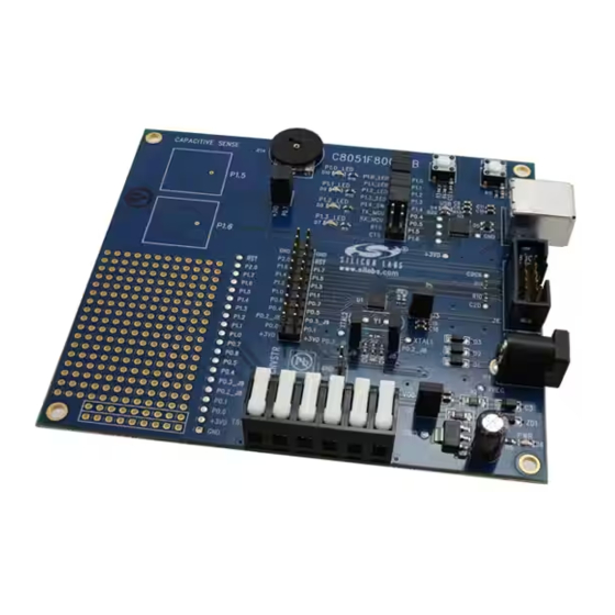
Page 7: Target Board
C8051F800-DK 7. Target Board The C8051F800 Development Kit includes a target board with a C8051F800-GM device pre-installed for evaluation and preliminary software development. Numerous input/output (I/O) connections are provided to facilitate prototyping using the target board. Refer to Figure 3 for the locations of the various I/O connectors. Figure 4 on page 8 shows the factory default shorting block positions. - Page 8 7.1. Target Board Shorting Blocks: Factory Defaults The C8051F800 Target Board comes from the factory with pre-installed shorting blocks on many headers. Figure 4 shows the positions of the factory default shorting blocks. It should be noted that a shorting block on J2 to connect power to the MCU is required for normal operation.
- Page 9 The on-chip crystal is accurate for many serial communications (UART, SPI, SMBus) and an external oscillator is not required depending on the bit rate. However, if you wish to operate the C8051F800 device at a frequency not available with the internal oscillator, an external crystal may be used. Refer to the C8051F80x-83x data sheet for more information on configuring the system clock source.
- Page 10 Two capacitive sense switches are also provided on the target board. The operation of these switches needs appropriate code running on the C8051F800 MCU that can sense the state of the switch. Note that no shorting blocks should be present on J3[15-16] and J3[17-18] for proper operation of these switches. See Section 6.3.
- Page 11 7.5. Target Board Debug Interface (J4) The DEBUG connector J4 provides access to the DEBUG (C2) pins of the C8051F800. It is used to connect the Serial Adapter or the USB Debug Adapter to the target board for in-circuit debugging and Flash programming.
- Page 12 C18 and C19, and also to TB1 pin 6 for an optional external VREF input. The J10 header connects P0.1 to GND, and is useful if the P0.1/AGND option is enabled via the REF0CN register in the C8051F800. Refer to the C8051F80x-83x data sheet for more information on configuring the voltage and ground reference options.
- Page 13 Some GPIO pins of the C8051F800 MCU can have an alternate fixed function. For example, pin 17on the C8051F800-GM MCU is designated P0.4, and can be used as a GPIO pin. Also, if the UART0 peripheral on the MCU is enabled using the crossbar registers, the TX signal is routed to this pin. This is shown in the "Alternate Fixed Function"...
- Page 14 C8051F800-DK 8. Schematics Rev. 0.2...
- Page 15 C8051F800-DK Rev. 0.2...
-
Page 16: Contact Information
Silicon Laboratories products are not designed, intended, or authorized for use in applications intended to support or sustain life, or for any other application in which the failure of the Silicon Laboratories product could create a situation where per- sonal injury or death may occur.
Need help?
Do you have a question about the C8051F800 and is the answer not in the manual?
Questions and answers