Table of Contents
Advertisement
Quick Links
Target Board Kit S5D5 (TB-S5D5)
Renesas Synergy™ Platform
Synergy Tools & Kits
Kits: TB-S5D5 v1.0
All information contained in these materials, including products and product specifications, represents
information on the product at the time of publication and is subject to change by Renesas Electronics
Corp. without notice. Please review the latest information published by Renesas Electronics Corp.
through various means, including the Renesas Electronics Corp. website (http://www.renesas.com).
www.renesas.com
User's Manual
Rev.1.02 Jul 2019
Advertisement
Table of Contents

Related Manuals for Renesas S5D5


Summary of Contents for Renesas S5D5
- Page 1 All information contained in these materials, including products and product specifications, represents information on the product at the time of publication and is subject to change by Renesas Electronics Corp. without notice. Please review the latest information published by Renesas Electronics Corp.
- Page 2 Renesas Electronics disclaims any and all liability for any damages or losses incurred by you or any third parties arising from the use of any Renesas Electronics product that is inconsistent with any Renesas Electronics data sheet, user’s manual or other Renesas Electronics document.
- Page 3 Terms and Conditions available at https://www.renesas.com/en-us/legal/disclaimer.html. The TB-S5D5 is not guaranteed to be error free, and the entire risk as to the results and performance of the TB-S5D5 is assumed by the User. The TB- S5D5 is provided by Renesas on an “as is” basis without warranty of any kind whether express or implied, including but not limited to the implied warranties of satisfactory quality, fitness for a particular purpose, title, and non-infringement of intellectual property rights with regard to the TB-S5D5.
-
Page 4: Table Of Contents
Target Board Kit S5D5 (TB-S5D5) Contents Overview ..........................3 Kit Contents ..........................6 Getting Started with Embedded Application Development on TB-S5D5 ........6 TB-S5D5 Hardware Details ..................... 6 Jumpers and DIP Switch Settings ......................6 4.1.1 Copper Jumpers ............................ 6 4.1.2... - Page 5 Renesas Synergy™ Platform Target Board Kit S5D5 (TB-S5D5) Additional Features ..........................25 5.6.1 Analog Reference Voltages ........................ 25 5.6.2 On-Board Clock Crystals ........................25 5.6.3 User Potentiometer ..........................26 5.6.4 Boot Configuration ..........................26 5.6.5 Miscellaneous Signals ......................... 27 5.6.5.1 AVCC0/AVSS0 ..........................27 5.6.5.2 VCL ..............................
-
Page 6: Overview
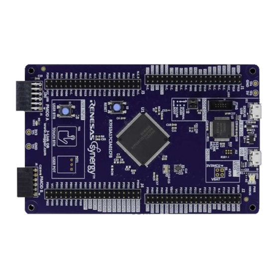
Renesas Synergy™ Platform Target Board Kit S5D5 (TB-S5D5) 1. Overview The Target Board Kit S5D5 (TB-S5D5) enables developers to get started with initial firmware development and evaluation of the Synergy Software Package (SSP) on the S5D3 MCU Group. • Renesas Synergy ™... - Page 7 Renesas Synergy™ Platform Target Board Kit S5D5 (TB-S5D5) Figure 1. TB-S5D5 Top Side R12UM0015EU0102 Rev.1.02 Page 4 of 35 Jul.10.19...
- Page 8 Renesas Synergy™ Platform Target Board Kit S5D5 (TB-S5D5) Figure 2. TB-S5D5 Bottom Side R12UM0015EU0102 Rev.1.02 Page 5 of 35 Jul.10.19...
-
Page 9: Kit Contents
Note: The TB-S5D5 uses J-Link On-board (OB) debug interface. While J-Link drivers are necessary to establish debug connection between the host PC and the TB-S5D5, they are not required to run the Out-of-Box (OoB) Demonstration (Blinky) Application that the TB-S5D5 comes pre-programmed with. -
Page 10: Default Board Configuration
Figure 3. Copper Jumpers 4.1.2 Default Board Configuration The following table describes the default settings for each jumper on the TB-S5D5. This includes traditional pin jumpers (Jx designation) and copper jumpers (Ex designation). The Circuit Group for each jumper is the designation found in the board schematic. See section 6, Electrical Schematics. - Page 11 Renesas Synergy™ Platform Target Board Kit S5D5 (TB-S5D5) Location Circuit Group Default Function Open/Closed ® J-Link OB USB Closed Connects the J-Link OB USB 5V input to the primary 5V->3.3V voltage regulator JTAG Connector Open JTAG Ground Detect. Connects the JTAG connector pin 9 to Ground.
-
Page 12: Hardware Layout
Renesas Synergy™ Platform Target Board Kit S5D5 (TB-S5D5) 5. Hardware Layout 5.1 System Block Diagram Figure 4. TB-S5D5 Block Diagram R12UM0015EU0102 Rev.1.02 Page 9 of 35 Jul.10.19... -
Page 13: Power Requirements
Target Board Kit S5D5 (TB-S5D5) 5.2 Power Requirements TB-S5D5 is designed for 3.3 V operation. This also means that 5 V PMOD devices cannot be used together with the TB-S5D5 unless they are powered separately. The total current available from the LDO regulator for all connected circuits is 600 mA or less, depending on the 5 V power source used. -
Page 14: Option 4: Pin Headers
Target Board Kit S5D5 (TB-S5D5) Figure 7. TP1, TP2, and LED1 on the Target Board These test points supply voltage directly to the S5D5 MCU, the S124 J-Link MCU, and other on-board circuitry. Use caution to ensure that any voltage connected in this manner meets the power requirements for the active features. -
Page 15: Powering Up The Board
The actual current consumed by the MCU can vary from less than 1 mA to nearly 40 mA. See the S5D5 Microcontroller Group User’s Manual for more information on the electrical characteristics of the MCU. -
Page 16: Main Components
5.3 Main Components • Main MCU Renesas Synergy™ S5D5 MCU device, part number R7FS5D5783A01CFP#AA0 (U1) • J-Link MCU Renesas Synergy™ S124 MCU device, part number R7FS124773A01CFM#AA0 (U2) • USB Connectors ... -
Page 17: Connectivity And Settings
Renesas Synergy™ Platform Target Board Kit S5D5 (TB-S5D5) • PMOD A Connector Samtec, part number SSW-106-02-F-D-RA (J5) • 12-pin right angle connector for PMOD A • PMOD B Connector Samtec, part number SSW-106-02-FM-S-RA (J6) • 6-pin right angle connector for PMOD B •... -
Page 18: Debug Usb
Renesas Synergy™ Platform Target Board Kit S5D5 (TB-S5D5) USB FS copper jumpers E16, E17, E20, and E21 configure the connection between the Device USB jack and the Main MCU. To allow use of the Device USB jack, copper jumper E16 and E17 must be closed, and copper jumpers E20 and E21 must be open. -
Page 19: Jtag/Swd
Renesas Synergy™ Platform Target Board Kit S5D5 (TB-S5D5) Table 5. DEBUG USB Connector (J11) DEBUG USB Connector TB-S5D5 Description Signal/Bus +5VDC +5V_JUSB Data- U2 USB_DM (U2-18) Data+ U2 USB_DP (U2-19) USB ID, jack internal switch, cable inserted N.C. Ground Three of the J-Link ports (P108, P109, and P300) conflict with the SPI interface, as shown in the following table. -
Page 20: Leds
5.4.4 LEDs Two LEDs are provided on the TB-S5D5. Target Board U1 is the Main MCU, and directly controls LED1. See Figure 7 for LED1 location, Figure 10 for LED2 location, and Figure 9 for LED2 circuit. Target Board U2 is the J-Link MCU, and controls the red LED in LED2. -
Page 21: Pmod A
Renesas Synergy™ Platform Target Board Kit S5D5 (TB-S5D5) Figure 15. User Switch Circuit Figure 16. User Switch (S1) on the Target Board Figure 17. Reset Switch Circuit Figure 18. Reset Switch (S2) on the Target Board 5.4.6 PMOD A A 12-pin PMOD type 2A connector is provided at PMOD A. The interface is powered for 3.3 V modules only. -
Page 22: Pmod B
Renesas Synergy™ Platform Target Board Kit S5D5 (TB-S5D5) Table 11. PMOD A Connector (J5) USB Device Connector TB-S5D5 Description Signal/Bus SS (low to select slave) U1 P103, SSLA0_A (U1-105) MOSI U1 P101, MOSIA_A (U1-107) MISO U1 P100, MISOA_A (U1-108) U1 P102, RSPCKA_A (U1-106) - Page 23 Renesas Synergy™ Platform Target Board Kit S5D5 (TB-S5D5) To disconnect the Capacitive Touch Button from the MCU, the copper jumper E2 must be open. To connect MCU signal P115 to pin header J3, the copper jumper E5 must be closed.
-
Page 24: Pin Headers
Target Boards for S1, S3, S5, S7 Synergy MCU Series. On the TB-S5D5, 40 pins of the pin headers are set aside for fixed function assignment. These pins are odd-numbered pins of J1 and even-numbered pins of J2. -
Page 25: Pin Header J1
Renesas Synergy™ Platform Target Board Kit S5D5 (TB-S5D5) Figure 24. Pin Header Circuits, J3 and J4 5.5.1 Pin Header J1 Pin header J1 is a 2-column by 20-row through-hole pin header on 2.54 mm centers. Table 15. Pin Header J1 Pin Assignment... -
Page 26: Pin Header J2
Renesas Synergy™ Platform Target Board Kit S5D5 (TB-S5D5) Color Key Primary Fixed Function Pins Secondary Fixed Function Pins 5.5.2 Pin Header J2 Pin header J2 is a 2-column by 20-row through-hole pin header on 2.54 mm centers. Table 16. Pin Header J2 Pin Assignment... -
Page 27: Pin Header J4
Renesas Synergy™ Platform Target Board Kit S5D5 (TB-S5D5) MCU Pin Signal Port J3 Pins Signal MCU Pin P307 P306 P305 P304 P303 P302 P112 P113 P114 P115 P608 P609 P610 P611 P612 P613 P614 Not Connected Not Connected Not Connected... -
Page 28: Additional Features
Not Connected Not Connected Color Key Secondary Fixed Function pins *Note: The S5D5 MCU does not support the SDHI WP signal, so J4-24 has been assigned an MCU GPIO signal. 5.6 Additional Features 5.6.1 Analog Reference Voltages A footprint for installation of capacitors C21 and C23 is provided on the Target Board. -
Page 29: User Potentiometer
Figure 26. User Potentiometer Circuit Figure 27. User Potentiometer on the Target Board (top) 5.6.4 Boot Configuration The BOOT CONFIG jumper, J8 is used to configure the operating mode of the S5D5 MCU at boot. Table 20. Boot Configuration Boot Configuration... -
Page 30: Miscellaneous Signals
Renesas Synergy™ Platform Target Board Kit S5D5 (TB-S5D5) Figure 29. Boot Mode Configuration Circuit 5.6.5 Miscellaneous Signals 5.6.5.1 AVCC0/AVSS0 By default, AVCC0 is connected to +3V3 MCU and AVSS0 is connected to the system ground. To disconnect these references from the AVCC0 and AVSS0 lines, copper jumpers E10 and E11 must be open. -
Page 31: Electrical Schematics
Renesas Synergy™ Platform Target Board Kit S5D5 (TB-S5D5) 6. Electrical Schematics R12UM0015EU0102 Rev.1.02 Page 28 of 35 Jul.10.19... - Page 32 Renesas Synergy™ Platform Target Board Kit S5D5 (TB-S5D5) R12UM0015EU0102 Rev.1.02 Page 29 of 35 Jul.10.19...
- Page 33 Renesas Synergy™ Platform Target Board Kit S5D5 (TB-S5D5) R12UM0015EU0102 Rev.1.02 Page 30 of 35 Jul.10.19...
- Page 34 Renesas Synergy™ Platform Target Board Kit S5D5 (TB-S5D5) R12UM0015EU0102 Rev.1.02 Page 31 of 35 Jul.10.19...
-
Page 35: Mechanical Drawing
Renesas Synergy™ Platform Target Board Kit S5D5 (TB-S5D5) 7. Mechanical Drawing If further details and dimensions are required, Gerber (RS 274X) and NC Drill files for this design are available at http://renesassynergy.com/kits/tb-s5d5 R12UM0015EU0102 Rev.1.02 Page 32 of 35 Jul.10.19... -
Page 36: Certifications
Renesas Synergy™ Platform Target Board Kit S5D5 (TB-S5D5) 8. Certifications FCC Compliance This device complies with part 15 of the FCC Rules. Operation is subject to the following two conditions: (1) This device may not cause harmful interference, and (2) This device must accept any interference received, including interference that may cause undesired operation. - Page 37 Renesas Synergy™ Platform Target Board Kit S5D5 (TB-S5D5) Website and Support Visit the following vanity URLs to learn about key elements of the Synergy Platform, download components and related documentation, and get support. Synergy Software www.renesas.com/synergy/software Synergy Software Package www.renesas.com/synergy/ssp Software add-ons www.renesas.com/synergy/addons...
-
Page 38: Revision History
Renesas Synergy™ Platform Target Board Kit S5D5 (TB-S5D5) Revision History Description Rev. Date Page Summary 1.00 Aug.24.17 Initial release 1.01 Dec.18.17 Replaced the graphics 1.02 Jul.10.19 Corrected typo for package type R12UM0015EU0102 Rev.1.02 Page 35 of 35 Jul.10.19... - Page 39 Target Board Kit S5D5 (TB-S5D5) User’s Manual Publication Date: Jul.10.19 Published by: Renesas Electronics Corporation...
- Page 40 Renesas Synergy™ Platform Target Board Kit S5D5 (TB-S5D5) R12UM0015EU0102...
- Page 41 Mouser Electronics Authorized Distributor Click to View Pricing, Inventory, Delivery & Lifecycle Information: Renesas Electronics YSTBS5D5E10...
Need help?
Do you have a question about the S5D5 and is the answer not in the manual?
Questions and answers