Table of Contents
Advertisement
Quick Links
Target Board Kit S3A1 (TB-S3A1)
Renesas Synergy™ Platform
Synergy Tools & Kits
Kits: TB-S3A1 v1.0
All information contained in these materials, including products and product specifications, represents
information on the product at the time of publication and is subject to change by Renesas Electronics
Corp. without notice. Please review the latest information published by Renesas Electronics Corp.
through various means, including the Renesas Electronics Corp. website (http://www.renesas.com).
www.renesas.com
Arrow.com.
Downloaded from
User's Manual
Rev.1.00 Feb 2018
Advertisement
Table of Contents

Related Manuals for Renesas Synergy S3A1


Summary of Contents for Renesas Synergy S3A1
- Page 1 All information contained in these materials, including products and product specifications, represents information on the product at the time of publication and is subject to change by Renesas Electronics Corp. without notice. Please review the latest information published by Renesas Electronics Corp.
- Page 2 Renesas Electronics products, such as safety design for hardware and software, including but not limited to redundancy, fire control and malfunction prevention, appropriate treatment for aging degradation or any other appropriate measures.
- Page 3 Renesas or its affiliates be liable for any other direct or indirect special, incidental or consequential damages arising out of or in relation to the use of this DK-S7G2, even if Renesas or its affiliates have been advised of the possibility of such damages.
-
Page 4: Table Of Contents
Target Board Kit S3A1 (TB-S3A1) Contents Contents 1. Overview .......................... 1 2. What’s in the box ......................4 3. Getting Started ........................ 4 Jumpers and DIP switch settings ......................4 Copper jumpers ..........................4 Default board configuration ......................5 4. Hardware Layout ......................7 System block diagram .......................... -
Page 5: Overview
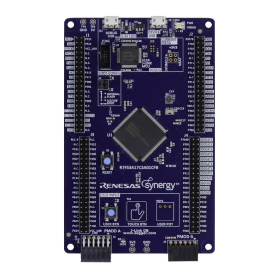
Target Board Kit S3A1 (TB-S3A1) Overview 1. Overview ™ The Target Board Kit-S3A1 (TB-S3A1) is a development kit for the Renesas Synergy S3A1 microcontroller in a LQFP144 package. TB-S3A1 is designed to help developers get started with initial firmware development and ™... - Page 6 Target Board Kit S3A1 (TB-S3A1) Overview Figure 1 TB-S3A1 Top Side R12UM0022EU0100 Rev.1.00 Page 2 of 36 Feb 6, 2018 Arrow.com. Arrow.com. Arrow.com. Arrow.com. Arrow.com. Arrow.com. Downloaded from Downloaded from Downloaded from Downloaded from Downloaded from Downloaded from...
- Page 7 Target Board Kit S3A1 (TB-S3A1) Overview Figure 2 TB-S3A1 bottom side R12UM0022EU0100 Rev.1.00 Page 3 of 36 Feb 6, 2018 Arrow.com. Arrow.com. Arrow.com. Arrow.com. Arrow.com. Arrow.com. Arrow.com. Downloaded from Downloaded from Downloaded from Downloaded from Downloaded from Downloaded from Downloaded from...
-
Page 8: What's In The Box
Target Board Kit S3A1 (TB-S3A1) What’s in the box 2. What’s in the box The following components are included in the kit: • TB-S3A1 Target Board Kit • One USB Type-A to Micro-B cable 3. Getting Started Before you start working with your kit, you need to obtain the latest version of the Synergy Software Package (SSP) and the development tools needed to work with it. -
Page 9: Default Board Configuration
Target Board Kit S3A1 (TB-S3A1) Getting Started 3.1.2 Default board configuration The following table describes the default settings for each jumper on the TB-S3A1 Target Board. This includes traditional pin jumpers (Jx designation) and copper jumpers (Ex designation.) The Circuit Group for each jumper is the designation found in the board schematic. (See Section 5: Electrical Schematics.) Functional details for many of the listed jumpers may be found in Section 4.4: Connectivity and Settings and Section 4.6: Additional Features. - Page 10 Target Board Kit S3A1 (TB-S3A1) Getting Started Location Circuit Group Default Function Open/Closed J-Link OB USB Closed Connects the J-Link OB USB 5V input to the primary 5V->3.3V voltage regulator JTAG Connector Open JTAG Ground Detect. Connects the JTAG connector pin 9 to Ground.
-
Page 11: Hardware Layout
Target Board Kit S3A1 (TB-S3A1) Hardware Layout 4. Hardware Layout System block diagram Power requirements TB-S3A1 is designed for 3.3 Volt operation. Note that this also means that 5V PMOD devices cannot be used together with the TB-S3A1 unless they are powered separately. The total current available from the LDO regulator for all connected circuits is 0.600A or less, depending the 5V power source used. -
Page 12: Power Supply Options
Target Board Kit S3A1 (TB-S3A1) Hardware Layout 4.2.1 Power supply options TB-S3A1 can be powered via several different methods: Option 1: Debug USB (Default) The default power source is 5V supplied from an external USB host to the USB Debug connector labelled DEBUG USB on the top surface of the board. - Page 13 Target Board Kit S3A1 (TB-S3A1) Hardware Layout These test points supply voltage directly to the S3A1 MCU, the S124 J-Link MCU, and other on-board circuitry. Use caution to ensure that any voltage connected in this manner meets the power requirements for the active features. Power sources that are outside of the published operating range for the active devices may cause degraded performance or damage the board.
-
Page 14: Power-Up Behavior
Target Board Kit S3A1 (TB-S3A1) Hardware Layout 4.2.2 Power-up behavior When powered, the green LED to the right of the DEVICE USB connector (LED2) lights up. The red LED in the same LED package functions as a status indicator for the J-Link On-Board debug interface on the board. -
Page 15: Major Components
The actual value selected should be based on the operating conditions of the MCU for your specific application, and the sensitivity of the measurement equipment used. Major components Main MCU • Renesas S3A1 MCU, part number R7FS3A17C3A01CFB#AA0 (U1) Main MCU J-Link MCU • Renesas S124 MCU, part number R7FS124773A01CFM#AA0 (U2) ... -
Page 16: Connectivity And Settings
Target Board Kit S3A1 (TB-S3A1) Hardware Layout Low-drop out linear regulator Generates system 3.3V from J-Link USB 5V input PMOD A Connector • Samtec, part number SSW-106-02-F-D-RA (J5) 12 pin right angle connector for PMOD A PMOD B Connector •... -
Page 17: Debug Usb
Target Board Kit S3A1 (TB-S3A1) Hardware Layout Table 2 Device USB connector (J9) USB device connector TB-S3A1 Description Signal/Bus +5VUSB +5VDC, connected to a sense voltage 2/3 divider to allow Main MCU sensing of Host presence P407/USB_VBUS = 2/3(5VUSB) Data- P915/USB_DM Data+ P914/USB_DP... -
Page 18: Jtag/Swd
Target Board Kit S3A1 (TB-S3A1) Hardware Layout Table 4 J-Link interface conflicts Programming Interface Conflicting Interface Port Interface P108 SWDIO / JTAG TMS SSLB0 fixed function, J1-13 P109 SWO / JTAG TDO MOSIB fixed function, J1-7 P300 SWCLK / JTAG TCK GTIOC0A fixed function, J1-31 4.4.3 JTAG/SWD... -
Page 19: Leds
Target Board Kit S3A1 (TB-S3A1) Hardware Layout Table 6 JTAG Interface Conflicts Programming Interface Conflicting Interface Port Interface P108 TMS / J-Link SWDIO SSLB0_B fixed function, J1-13 P109 TDO / J-Link SWO MOSIB_B fixed function, J1-7 P110 MISOB_B fixed function, J1-9 P300 SWCLK GTIOC0A_A fixed function, J1-31... - Page 20 Target Board Kit S3A1 (TB-S3A1) Hardware Layout Table 8 Target board switches Designator Function MCU Control Port MCU Pin User Switch U1 P105/IRQ0 U1-103 MCU Reset Switch RESET# U1-55 Figure 13 User switch circuit Figure 14 User switch (S1) on target board Figure 15 Reset switch circuit Figure 16 Reset switch (S2) on target board R12UM0022EU0100 Rev.1.00...
-
Page 21: Pmod A
Target Board Kit S3A1 (TB-S3A1) Hardware Layout 4.4.6 PMOD A A 12-pin PMOD type 2A connector is provided at PMOD A. The interface is powered for 3.3V modules only. The Main MCU acts as the SPI master, and the connected module acts as an SPI slave device. This interface may additionally be re-configured in firmware as several other PMOD types. -
Page 22: User Capacitive Touch Button
Target Board Kit S3A1 (TB-S3A1) Hardware Layout PMOD B connector TB-S3A1 Description Signal/Bus +3V3 Limits of the 3.3V regulator on the Target Board, and limits of the power source supplying that regulator (especially for USB Host devices), including the to-be-connected PMOD device, must be considered prior to connecting a module to a PMOD connector. -
Page 23: Target Board Pin Headers
Target Board Kit S3A1 (TB-S3A1) Hardware Layout Figure 18 Capacitive touch TSCAP circuit Figure 19 Capacitive touch button on target board (top) Target board pin headers The Target Board pin headers, J1, J2, J3, and J4, provide access to all Main MCU interface signals, and to voltages for all Main MCU power ports. - Page 24 Target Board Kit S3A1 (TB-S3A1) Hardware Layout Figure 20 Fixed function pin label example There are several pins in the headers that are secondary fixed function pins. These secondary fixed function pins share common pin assignments with other Target Boards having the Main MCUs with the same functionality. The secondary fixed function pins are also labeled with top side having a functional label, and bottom side having a port label.
-
Page 25: Pin Header J1
Target Board Kit S3A1 (TB-S3A1) Hardware Layout 4.5.1 Pin header J1 Pin header J1 is a 2-column by 20-row through-hole header on 0.100 inch centers. Table 12 Pin header J1 pin assignment 144p 144p S3A1 Pin S3A1 Signal J1 Pins S3A1 Signal S3A1 Pin P100... -
Page 26: Pin Header J2
Target Board Kit S3A1 (TB-S3A1) Hardware Layout 4.5.2 Pin header J2 Pin header J2 is a 2-column by 20-row through-hole header on 0.100 inch centers. Table 13 Pin header J2 pin assignment 144p S3A1 144p S3A1 Signal J2 Pins S3A1 Signal S3A1 Pin P414 P410... -
Page 27: Pin Header J3
Target Board Kit S3A1 (TB-S3A1) Hardware Layout 4.5.3 Pin header J3 Pin header J3 is a 2-column by 20-row through-hole header on 0.100 inch centers. Table 14 Pin Header J3 pin assignment 144p 144p S3A1 Pin S3A1 Signal J3 Pins S3A1 Signal S3A1 Pin (None) -
Page 28: Pin Header J4
Target Board Kit S3A1 (TB-S3A1) Hardware Layout 4.5.4 Pin header J4 Pin header J4 is a 2-column by 20-row through-hole header on 0.100 inch centers. Table 15 Pin Header J4 pin assignment 144p 144p S3A1 Pin S3A1 Signal J4 Pins S3A1 Signal S3A1 Pin P704... -
Page 29: On-Board Clock Crystals
Target Board Kit S3A1 (TB-S3A1) Hardware Layout installation of capacitor C21 can reduce reference voltage noise and improve ADC measurement and DAC output quality. The Target Board was designed for Samsung P/N CL10B104KB8NNNC, or similar, noise-bypass capacitors. Port pair P012/P013 may be assigned as GPIO, where bypass capacitor C23 would damage signal quality. When P012/P013 are to be assigned as VREFH/VREFL, installation of capacitor C23 may reduce reference voltage noise and improve ADC measurement and DAC output quality. -
Page 30: Boot Configuration
Target Board Kit S3A1 (TB-S3A1) Hardware Layout Figure 23 User potentiometer circuit Figure 24 User potentiometer on the target board (top) 4.6.4 Boot configuration The BOOT CONFIG jumper, J8, is used to configure the operating mode of the S3A1 MCU at boot. Table 17 Boot configuration Boot Configuration J8 Shunt Location... - Page 31 Target Board Kit S3A1 (TB-S3A1) Hardware Layout 4.6.5.2 By default, the Main MCU pin VCL is connected to reference capacitor C17. To connect this pin to MCU pin header J2, solder bridge E28 must be closed. To disconnect the reference capacitor C17, copper jumper E29 must be open.
-
Page 32: Electrical Schematics
Target Board Kit S3A1 (TB-S3A1) 5. Electrical Schematics R12UM0022EU0100 Rev.1.00 Arrow.com. Arrow.com. Arrow.com. Arrow.com. Arrow.com. Arrow.com. Arrow.com. Arrow.com. Arrow.com. Arrow.com. Arrow.com. Arrow.com. Arrow.com. Arrow.com. Arrow.com. Arrow.com. Arrow.com. Arrow.com. Arrow.com. Arrow.com. Arrow.com. Arrow.com. Arrow.com. Arrow.com. Arrow.com. Arrow.com. Arrow.com. Arrow.com. Arrow.com. Arrow.com. Arrow.com. - Page 33 Target Board Kit S3A1 (TB-S3A1) R12UM0022EU0100 Rev.1.00 Arrow.com. Arrow.com. Arrow.com. Arrow.com. Arrow.com. Arrow.com. Arrow.com. Arrow.com. Arrow.com. Arrow.com. Arrow.com. Arrow.com. Arrow.com. Arrow.com. Arrow.com. Arrow.com. Arrow.com. Arrow.com. Arrow.com. Arrow.com. Arrow.com. Arrow.com. Arrow.com. Arrow.com. Arrow.com. Arrow.com. Arrow.com. Arrow.com. Arrow.com. Arrow.com. Arrow.com. Arrow.com. Arrow.com. Downloaded from Downloaded from Downloaded from...
- Page 34 Target Board Kit S3A1 (TB-S3A1) R12UM0022EU0100 Rev.1.00 Arrow.com. Arrow.com. Arrow.com. Arrow.com. Arrow.com. Arrow.com. Arrow.com. Arrow.com. Arrow.com. Arrow.com. Arrow.com. Arrow.com. Arrow.com. Arrow.com. Arrow.com. Arrow.com. Arrow.com. Arrow.com. Arrow.com. Arrow.com. Arrow.com. Arrow.com. Arrow.com. Arrow.com. Arrow.com. Arrow.com. Arrow.com. Arrow.com. Arrow.com. Arrow.com. Arrow.com. Arrow.com. Arrow.com. Arrow.com.
- Page 35 Target Board Kit S3A1 (TB-S3A1) R12UM0022EU0100 Rev.1.00 Arrow.com. Arrow.com. Arrow.com. Arrow.com. Arrow.com. Arrow.com. Arrow.com. Arrow.com. Arrow.com. Arrow.com. Arrow.com. Arrow.com. Arrow.com. Arrow.com. Arrow.com. Arrow.com. Arrow.com. Arrow.com. Arrow.com. Arrow.com. Arrow.com. Arrow.com. Arrow.com. Arrow.com. Arrow.com. Arrow.com. Arrow.com. Arrow.com. Arrow.com. Arrow.com. Arrow.com. Arrow.com. Arrow.com. Arrow.com.
- Page 36 Target Board Kit S3A1 (TB-S3A1) R12UM0022EU0100 Rev.1.00 Arrow.com. Arrow.com. Arrow.com. Arrow.com. Arrow.com. Arrow.com. Arrow.com. Arrow.com. Arrow.com. Arrow.com. Arrow.com. Arrow.com. Arrow.com. Arrow.com. Arrow.com. Arrow.com. Arrow.com. Arrow.com. Arrow.com. Arrow.com. Arrow.com. Arrow.com. Arrow.com. Arrow.com. Arrow.com. Arrow.com. Arrow.com. Arrow.com. Arrow.com. Arrow.com. Arrow.com. Arrow.com. Arrow.com. Arrow.com.
-
Page 37: Mechanical Drawing
Target Board Kit S3A1 (TB-S3A1) Mechanical Drawing 6. Mechanical Drawing R12UM0022EU0100 Rev.1.00 Page 33 of 36 Feb 6, 2018 Arrow.com. Arrow.com. Arrow.com. Arrow.com. Arrow.com. Arrow.com. Arrow.com. Arrow.com. Arrow.com. Arrow.com. Arrow.com. Arrow.com. Arrow.com. Arrow.com. Arrow.com. Arrow.com. Arrow.com. Arrow.com. Arrow.com. Arrow.com. Arrow.com. Arrow.com. - Page 38 Position is shown as (#,#), where the first number is distance from the left Target Board edge and the second number is distance from the lower Target Board edge (board viewed with “Renesas” oriented for normal viewing), board viewed from its top surface.
-
Page 39: Certifications
Target Board Kit S3A1 (TB-S3A1) Certifications 7. Certifications FCC Compliance This device complies with part 15 of the FCC Rules. Operation is subject to the following two conditions: (1) This device may not cause harmful interference, and (2) this device must accept any interference received, including interference that may cause undesired operation. -
Page 40: Additional Resources
8. Additional Resources For more information on how to order this kit from Renesas or from a local distributor, visit the kit page on our website. In addition to ordering information, you will also be able to download schematics, relevant application projects, technical updates and more: TB-S3A1 Kit page: http://renesassynergy.com/kits/TB-S3A1... - Page 41 Revision History Description Rev. Date Page Summary 1.00 Feb 6, 2017 Initial release All trademarks and registered trademarks are the property of their respective owners. Arrow.com. Arrow.com. Arrow.com. Arrow.com. Arrow.com. Arrow.com. Arrow.com. Arrow.com. Arrow.com. Arrow.com. Arrow.com. Arrow.com. Arrow.com. Arrow.com. Arrow.com. Arrow.com.
- Page 42 Target Board Kit S3A1 (TB- S3A1) User’s Manual Publication Date: Rev.1.00 Feb 6, 2018 Published by: Renesas Electronics Corporation Arrow.com. Arrow.com. Arrow.com. Arrow.com. Arrow.com. Arrow.com. Arrow.com. Arrow.com. Arrow.com. Arrow.com. Arrow.com. Arrow.com. Arrow.com. Arrow.com. Arrow.com. Arrow.com. Arrow.com. Arrow.com. Arrow.com. Arrow.com. Arrow.com.
- Page 43 SALES OFFICES Refer to "http://www.renesas.com/" for the latest and detailed information. Renesas Electronics America Inc. 1001 Murphy Ranch Road, Milpitas, CA 95035, U.S.A. Tel: +1-408-432-8888, Fax: +1-408-434-5351 Renesas Electronics Canada Limited 9251 Yonge Street, Suite 8309 Richmond Hill, Ontario Canada L4C 9T3...
- Page 44 Renesas Synergy™ Platform Target Board Kit S3A1 (TB-S3A1) R12UM0022EU0100 Arrow.com. Arrow.com. Arrow.com. Arrow.com. Arrow.com. Arrow.com. Arrow.com. Arrow.com. Arrow.com. Arrow.com. Arrow.com. Arrow.com. Arrow.com. Arrow.com. Arrow.com. Arrow.com. Arrow.com. Arrow.com. Arrow.com. Arrow.com. Arrow.com. Arrow.com. Arrow.com. Arrow.com. Arrow.com. Arrow.com. Arrow.com. Arrow.com. Arrow.com. Arrow.com. Arrow.com.
Need help?
Do you have a question about the Synergy S3A1 and is the answer not in the manual?
Questions and answers