Renesas RA4 Series User Manual
Evaluation kit for ra4m2 microcontroller group
Hide thumbs
Also See for RA4 Series:
- User manual (1317 pages) ,
- Quick start manual (28 pages) ,
- Engineering manual (17 pages)
Table of Contents
Advertisement
Quick Links
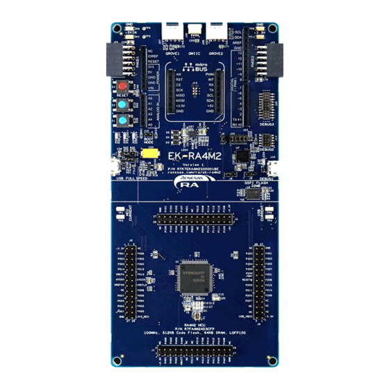
RA4M2 Group
Evaluation Kit for RA4M2 Microcontroller Group
Renesas RA Family
RA4 Series
All information contained in these materials, including products and product specifications, represents
information on the product at the time of publication and is subject to change by Renesas Electronics
Corp. without notice. Please review the latest information published by Renesas Electronics Corp.
through various means, including the Renesas Electronics Corp. website (http://www.renesas.com).
www.renesas.com
EK-RA4M2 v1
User's Manual
Rev. 1.00 Jan 2021
Advertisement
Table of Contents


Need help?
Do you have a question about the RA4 Series and is the answer not in the manual?
Questions and answers