Analog Devices SDP-S User Manual

Analog Devices SDP-S User Manual

Controller board

Advertisement

One Technology Way • P.O. Box 9106 • Norwood, MA 02062-9106, U.S.A. • Tel: 781.329.4700 • Fax: 781.461.3113 • www.analog.com

FEATURES

USB-to-serial engine
Peripherals exposed
SPI
TWI/I
2
C
GPIO
USB 2.0 PC connectivity
PC software stack and base firmware provided

GENERAL DESCRIPTION

This user guide describes the EVAL-SDP-CS1Z system
demonstration platform-serial (SDP-S) controller board from
Analog Devices, Inc. The SDP-S controller board is part of the
Analog Devices system demonstration platform (SDP). The
SDP consists of a series of controller boards, interposer boards,
and daughter boards. SDP controller boards provide a means
of communicating with the system under evaluation from the
PC. Interposer boards route signals between two connectors.
Daughter boards are a collection of product evaluation boards
and Circuits from the Lab™ reference circuit boards. The SDP-S
is used as part of the evaluation system for many Analog Devices
components and reference circuits. The primary audience for
this user guide is the system engineer who seeks to understand
PLEASE SEE THE LAST PAGE FOR AN IMPORTANT
WARNING AND LEGAL TERMS AND CONDITIONS.
SDP-S Controller Board
how to set up the SDP-S board and begin USB communications
to the PC.
The SDP-S board is designed to be used in conjunction with
various Analog Devices component evaluation boards and
Circuits from the Lab reference circuits as part of a customer
evaluation environment. The SDP-S provides USB connectivity
through a USB 2.0 high speed connection to the computer,
allowing users to evaluate components on this platform from a
PC application. The SDP-S is based on a USB-to-serial engine,
which has SPI, I
small footprint connector.
This user guide provides instructions for installing the SDP-S
hardware (EVAL-SDP-CS1Z board) and software onto a
computer. The necessary installation files are provided with the
evaluation daughter board package. The Getting Started section
provides software and hardware installation procedures, PC
system requirements, and basic board information. The Evaluation
Board Hardware section provides information on the EVAL-
SDP-CS1Z components. The EVAL-SDP-CS1Z schematics are
provided in the Evaluation Board Schematics section.
For more information about the SDP-S board, go to
www.analog.com/sdp.
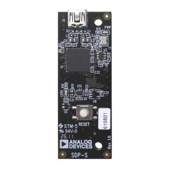
Figure 1. Picture of EVAL-SDP-CS1Z
Rev. A | Page 1 of 16
SDP-S User Guide
C, and GPIO lines available, with a 120-pin
2
UG-291

Advertisement

Table of Contents
loading
Need help?

Need help?

Do you have a question about the SDP-S and is the answer not in the manual?

Questions and answers

Summary of Contents for Analog Devices SDP-S

  • Page 1: Features

    One Technology Way • P.O. Box 9106 • Norwood, MA 02062-9106, U.S.A. • Tel: 781.329.4700 • Fax: 781.461.3113 • www.analog.com SDP-S Controller Board FEATURES how to set up the SDP-S board and begin USB communications to the PC. USB-to-serial engine...
  • Page 2: Table Of Contents

    SDP-S User Guide TABLE OF CONTENTS Features ....................1 USB Installation ................4 General Description ................. 1 Powering Up/Powering Down the SDP-S ........4 Revision History ................2 Evaluation Board Hardware .............5 Product Overview ................3 LEDs ....................5 Package Contents ................3 Connector Details .................5...
  • Page 3: Product Overview

    Visit MyAnalog.com to sign up. If you are a registered user, Contact the vendor where the SDP-S board was purchased, or simply log on. Your user name is your email address. contact Analog Devices if anything is missing. TECHNICAL OR CUSTOMER SUPPORT...
  • Page 4: Getting Started

    Connecting the SDP-S Board to the PC Connect the SDP-S board to the daughter evaluation board through the 120-pin mating connector. Attach the SDP-S board to a USB 2.0 port on the computer via Power up the daughter board. the Standard-A-to-Mini-B cable provided.
  • Page 5: Evaluation Board Hardware

    LEDS Connector Pin Assignments There are two LEDs located on the SDP-S board (see Figure 3). Table 1 lists the connector pins and identifies the functionality Power LED (PWR) assigned to each connector pin on the SDP-S board.
  • Page 6 UG-291 SDP-S User Guide Table 1. 120-Pin Connector Pin Assignments Pin No. Pin Name Description No connect. Leave this pin unconnected. Do not ground. No connect. Leave this pin unconnected. Do not ground. Connect to the ground plane of the daughter board.
  • Page 7 EEPROM A0. Connect to the A0 address line of the EEPROM. RESET_OUT Active low pin for resetting the daughter board. Driven by SDP-S. Connect to the ground plane of the daughter board. Do not use. Leave this pin unconnected. Do not ground.
  • Page 8 UG-291 SDP-S User Guide Pin No. Pin Name Description Do not use. Leave this pin unconnected. Do not ground. Do not use. Leave this pin unconnected. Do not ground. Do not use. Leave this pin unconnected. Do not ground. Connect to the ground plane of the daughter board.
  • Page 9 SDP-S User Guide UG-291 Each interface provided by the SDP-S is available on unique pins of the SDP-S 120-pin connector. The connector pin numbering scheme is outlined in Figure 4. RESET_IN RESET_OUT EEPROM_A0 SDP-S CONNECTOR GPIO6 GPIO7 GENERAL GPIO4 GPIO5...
  • Page 10: Power

    POWER The daughter board connector and securing screw holes are The SDP-S board is powered by the USB connector. It does not located in the top left hand corner. This arrangement for a require power to be supplied by the daughter board. The SDP-S daughter board is shown in Figure 5.
  • Page 11: Mechanical Specifications

    The keep out area is 12.65 mm wide and extends down the MECHANICAL SPECIFICATIONS entire left side of the daughter board. The mechanical specifications of the SDP-S board are 2.36 inch Restriction on Right Angle Connectors × 0.87 inch (60 mm × 22 mm). The tallest component on the top is approximately 0.17 inch (4.3 mm), and the tallest compo-...
  • Page 12 UG-291 SDP-S User Guide 0.87” 22.0 mm POWER 2.36” 60.0mm RESET BUTTON RESET BUTTON 0.17” / 4.3mm 0.238” / 6.05mm CON A 0.152” / 3.86mm CON A Figure 7. SDP-S Board Mechanical Specifications Rev. A | Page 12 of 16...
  • Page 13: Evaluation Board Schematics

    SDP-S User Guide UG-291 EVALUATION BOARD SCHEMATICS This section provides the schematic drawings for the EVAL-SDP-CB1Z board, which include • SDP-S—USB-to-serial engine, USB, interface (see Figure 8) • SDP-S—Connector (see Figure 9) Rev. A | Page 13 of 16...
  • Page 14 UG-291 SDP-S User Guide Figure 8. SDP-S—USB-to-Serial Engine, USB, Interface Rev. A | Page 14 of 16...
  • Page 15 SDP-S User Guide UG-291 J1-1 J1-2 VBUS J1-56 TWI_A0 ADP121 J1-116 100kΩ PWR_EN 100nF 100nF J1-60 RESET_IN J1-57 RESET_OUT RESET_OUT J1-64 SLEEP SLEEP J1-65 0Ω WAKE MIC2025-1YMM J1-61 BMODE1_A USB_VBUS VBUS J1-5 PWR_EN J1-92 SPORT_RSCLK J1-90 SPORT_RFS J1-91 SPORT_DR0 100nF...
  • Page 16 By using the evaluation board discussed herein (together with any tools, components documentation or support materials, the “Evaluation Board”), you are agreeing to be bound by the terms and conditions set forth below (“Agreement”) unless you have purchased the Evaluation Board, in which case the Analog Devices Standard Terms and Conditions of Sale shall govern. Do not use the Evaluation Board until you have read and agreed to the Agreement.

This manual is also suitable for:

Eval-sdp-cs1z803-1734

Table of Contents