Table of Contents
Advertisement
Quick Links
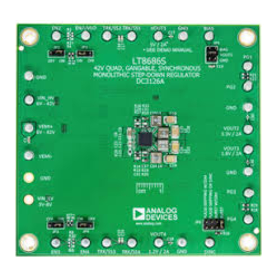
DESCRIPTION
Demonstration circuit 3126A is a quad power supply fea-
turing the
LT
8686S. The LT8686S is a 42V quad channel
®
current mode monolithic synchronous step-down regu-
lator. The LT8686S combines two 42V capable 2A buck
regulators with two 8V capable 2A buck regulators. The
demo board is designed for 5V, 3.3V, 1.8V, and 1.2V out-
puts from a nominal 12V input with switching frequency
set at 2MHz. The 5V and 3.3V converters are powered
from a wide range of 6V to 42V. The 1.8V and 1.2V con-
verters are powered from the 5V output by default or from
3V to 8V supply alternatively. The current capability is 2A
for all 4 outputs when running individually.
The DC3126A provides two 42V regulators that can be
combined to deliver up to 4A of output current using a
singular inductor. Similarly, the two 8V regulators can be
combined to deliver up to 4A of output current using a
singular inductor. The allowed channel combinations are
given in the data sheet.
The independent track/soft-start and power good for each
output simplify the complex design of quad-output power
converters. Each output can be independently disabled
into low quiescent current shutdown mode with its own
TRK/SS pin.
A user-selectable SYNC/MODE pin on the demo board
provides two primary modes of operation: pulse-skip-
ping mode and low ripple Burst Mode
the option of selecting frequency spread-spectrum for
each to improve the EMI/EMC performance. Burst Mode
42V Quad, Gangable, Synchronous, Monolithic
operation, plus
®
DEMO MANUAL DC3126A
Step-Down Regulator
delivers higher efficiency at light load than pulse-skipping
mode. In pulse-skipping mode, full switching frequency
is maintained to lower load currents than Burst Mode.
The SYNC/MODE pin can also be used to synchronize the
switching frequency to an external clock. The switching
frequency for all regulators can be programmed either via
an oscillator resistor or an external clock over a 350kHz
to 3MHz range. At all frequencies, a 180° phase shift is
maintained between channel 1 and channel 2, channel 3
and channel 4, reducing the input peak current and volt-
age ripple.
The demo board has an EMI filter installed on the bottom
layer. The conducted and radiated EMI performance of
the board is shown on Figure 4. The red line in Figure 4
is CISPR25 Class 5 peak limit. The figure shows that the
circuit passes the test with a wide margin. To achieve EMI/
EMC performance as shown in Figure 4, the input EMI
filter is required, and the input voltage should be applied
at VEMI turret.
The LT8686S data sheet gives a complete description of
the part operation and application information. The data
sheet must be read in conjunction with this quick start
guide for DC3126A. The LT8686S is assembled in a 5mm
× 5mm LQFN package with exposed pads for low thermal
resistance. Proper board layout is essential for both low
EMI operation and best thermal performance.
Design files for this circuit board are
All registered trademarks and trademarks are the property of their respective owners.
LT8686S
available.
Rev. 0
1
Advertisement
Table of Contents

Related Manuals for Analog Devices DC3126A


Summary of Contents for Analog Devices DC3126A
- Page 1 TRK/SS pin. guide for DC3126A. The LT8686S is assembled in a 5mm × 5mm LQFN package with exposed pads for low thermal A user-selectable SYNC/MODE pin on the demo board resistance.
-
Page 2: Performance Summary
DEMO MANUAL DC3126A PERFORMANCE SUMMARY Specifications are at T = 25°C SYMBOL PARAMETER CONDITIONS UNITS HV Regulators Input Voltage (V ) Range IN_HV LV Regulators Input Voltage (V ) Range IN_LV Output1 Voltage = 12V OUT1 IN_HV Output2 Voltage = 12V 3.17... - Page 3 (R31, R32). Keep the resistor divider 4, can operate with different input voltages instead networks on the main channels and remove the of 5V VOUT1. The DC3126A provides and onboard resistor divider networks on subordinate channels. 0Ω jumper (R29) to connect VIN_LV to VOUT1 by default.
- Page 4 DEMO MANUAL DC3126A QUICK START PROCEDURE Figure 1. Proper Measurement Equipment Setup – Figure 2. Scope Probe Placement for Measuring Input or Output Voltage Ripple Rev. 0...
-
Page 5: Typical Performance Characteristics
DEMO MANUAL DC3126A TYPICAL PERFORMANCE CHARACTERISTICS HV Channel Efficiency vs HV Channel Efficiency vs Load Current Load Current = 12V, V = 5V = 12V, V = 3.3V IN_HV OUT1 IN_HV OUT2 = 24V, V = 5V = 24V, V = 3.3V... - Page 6 DEMO MANUAL DC3126A TYPICAL PERFORMANCE CHARACTERISTICS Conducted EMI Performance CLASS 5 PEAK LIMIT –10 SPREAD SPECTRUM MODE FIXED FREQUENCY MODE –20 FREQUENCY (MHz) dc3126a F04a Radiated EMI Performance – Horizontal Polarization Radiated EMI Performance – Vertical Polarization (CISPR25 Radiated Emission Test with...
-
Page 7: Parts List
DEMO MANUAL DC3126A PARTS LIST ITEM REFERENCE PART DESCRIPTION MANUFACTURER/PART NUMBER Required Circuit Components C1, C13 CAP ., 1µF, X5R, 50V, 10%, 0603 MURATA, GRT188R61H105KE13D C2, C3, C6, C7, C9, C11 CAP ., 0.1µF, X7R, 50V, 10%, 0402 MURATA, GCM155R71H104KE02D C4, C5 CAP ., 10µF, X7R, 50V, 10%, 1210... - Page 8 DEMO MANUAL DC3126A PARTS LIST ITEM REFERENCE PART DESCRIPTION MANUFACTURER/PART NUMBER Additional Demo Board Circuit Components CAP ., 22µF, 35V, 20%, SMD, RADIAL, CE-BSS SERIES SUN ELECTRONIC INDUSTRIES CORP , 35CE22BSS R9, R12, R15, R18 RES., OPTION, 0402 R2, R4, R6, R8, R27, R30, RES., OPTION, 0603...
-
Page 9: Schematic Diagram
Devices for its use, nor for any infringements of patents or other rights of third parties that may result from its use. Specifications subject to change without notice. No license is granted by implication or otherwise under any patent or patent rights of Analog Devices. - Page 10 Board until you have read and agreed to the Agreement. Your use of the Evaluation Board shall signify your acceptance of the Agreement. This Agreement is made by and between you (“Customer”) and Analog Devices, Inc. (“ADI”), with its principal place of business at One Technology Way, Norwood, MA 02062, USA. Subject to the terms and conditions of the Agreement, ADI hereby grants to Customer a free, limited, personal, temporary, non-exclusive, non-sublicensable, non-transferable license to use the Evaluation Board FOR EVALUATION PURPOSES ONLY.
Need help?
Do you have a question about the DC3126A and is the answer not in the manual?
Questions and answers