Advertisement
DESCRIPTION
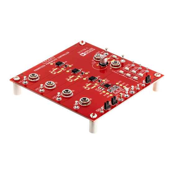
Demonstration circuit DC1717B uses the
arbitrate between three input supply rails, selecting the
highest priority, valid supply to power the load. The rail's
priority is defined by the input connection (V1-V3). Each
rail has overvoltage and undervoltage thresholds set by
external resistors. If the highest priority rail voltage falls
out of the defined window (overvoltage or undervoltage),
the rail with the next highest priority, which is valid, is
PERFORMANCE SUMMARY
SYMBOL
PARAMETER
V1-V3, V
V1 to V3, V
OUT
OUT
ΔV
Open (VS-VG) Clamp Voltage
G
ΔV
Sourcing (VS-VG) Clamp Voltage
G(SOURCE)
ΔV
Sinking (VS-VG) Clamp Voltage
G(SINK)
ΔV
G1 to G3 Off (VS-VG) Threshold
G(OFF)
ΔV
G1 to G3 Pull-Down Slew Rate
G(SLEW,ON)
ΔV
G1 to G3 Pull-Up Slew Rate
G(SLEW,OFF)
I
G1 to G3 Low Pull-Down Current
GATE(LOW)
V
Reverse Voltage Threshold
REV
t
Break-Before-Make Time
G(SWITCHOVER)
V
VALID1 to VALID3 Output Low Voltage
VALID(OL)
t
VALID1 to VALID3 Delay OFF from
PVALID(OFF)
OV/UV Fault
V
SHDN Threshold Voltage
SHDN(THR)
V
SHDN, EN Threshold Hysteresis
SHDN_EN(HYS)
I
SHDN, EN Pull-Up Current
SHDN_EN
V
OV1 to O3, UV1 to UV3 Comparator
OV_UV(THR)
Threshold
V
OV1 to O3, UV1 to UV3 Comparator
OV_UV(HYS)
Hysteresis
t
V1 to V3 Validation Time
VALID
V1
Operating Voltage of Channel V1
V2
Operating Voltage of Channel V2
V3
Operating voltage of Channel V3
I
Load Current
LOAD
AVI
Auxiliary Voltage Input
Prioritized PowerPath™ Controller
LTC
4417
®
Specifications are at T
CONDITIONS
Operating Supply Range
V
OUT
V
OUT
V
OUT
V1 = V2 = V3 = 2.8V, V
V
OUT
V
OUT
V
OUT
Measure (V1 to V3) – V
V
OUT
I = 1mA, (V1 to V3) = 2.5V, V
SHDN Rising
SHDN = EN = 0V
V
OUT
V
OUT
DEMO MANUAL DC1717B
to
enabled and powers the load. Two or more LTC4417s
can be cascaded to provide switchover between more
than three rails.
Design files for this circuit board are available at
www.analog.com/DC1717B.
= 25°C
A
= 11V, G1 to G3 = Open
= 11V, I = –10µA
= 11V, I = 10µA
= 2.6V, G1 to G3 Rising Edge
OUT
= 11V, C
= 10nF
GATE
= 11V, C
= 10nF
GATE
= 2.6V, V1 to V3 = 2.8V, (G1 to G3) = ΔV
, V
Falling
OUT
OUT
= 11V, C
= 10nF
GATE
= 0V
OUT
= 11V, OV1 to OV3 Rising, UV1 to UV3 Falling
= 11V
LTC4417
MIN
TYP
2.5
5.4
6.2
5.8
6.6
4.5
5.2
0.12
0.35
4
9
7.5
13
+ 300mV
0.8
2
G
30
120
0.7
2
0.2
5
8
0.4
0.8
100
–0.5
–2
0.985
1
15
30
100
256
9.6
12
4
5
6.4
8
2
6
MAX
UNITS
36
V
6.7
V
7
V
6
V
0.6
V
20
V/µs
22
V/µs
7
µA
200
mV
3
µs
0.55
V
13
µs
1.2
V
mV
–5
µA
1.015
V
45
mV
412
ms
14.4
V
6
V
9.6
V
A
24
V
Rev 0
1
Advertisement
Table of Contents

Related Manuals for Analog Devices DC1717B


Summary of Contents for Analog Devices DC1717B
- Page 1 DEMO MANUAL DC1717B LTC4417 Prioritized PowerPath™ Controller DESCRIPTION Demonstration circuit DC1717B uses the 4417 enabled and powers the load. Two or more LTC4417s ® arbitrate between three input supply rails, selecting the can be cascaded to provide switchover between more highest priority, valid supply to power the load.
-
Page 2: Operating Principles
V1, V2, and V3 voltages. regulated by an LT3060 (U4) to 5V. This auxiliary 5V rail DC1717B is designed to operate from inputs of 12V, also powers 100kΩ pull-ups for VALID pins. AVI must be present in order for the board to operate. See the Modifica- 5V, and 8V, applied to V1, V2 and V3 respectively. - Page 3 47µF during transient, and the value of load capacitance. Figure 1 DESIGN PROCEDURE FOR MODIFICATION OF DC1717B The valid input range for any supply is controlled by the The slew rate of the output voltage can be expressed as OV and UV comparators with resistive dividers (R4-R13).
- Page 4 DEMO MANUAL DC1717B DESIGN PROCEDURE FOR MODIFICATION OF DC1717B The second summand, t , should be taken into As shown in the equation (3), the use of external slew rate pVALID(OFF) account if the associated LTC4417 input does not have...
- Page 5 LEDs and pull ups. Use this turret to verify that 5V CAS: used to cascade a second DC1717B. Connect the is present. CAS turret of the high priority DC1717B to the EN turret of the lower priority DC1717B. Grounds must be connected in common.
-
Page 6: Quick Start Procedure
Connecting the auxiliary power source (6V to 24V) to Placing the jumper JP2 (EN) in the ON position turns on the DC1717B (AVI and GND turrets) lights the green LED the LTC4417 powering the load with 12V (2.0A). In an... -
Page 7: Parts List
DEMO MANUAL DC1717B PARTS LIST ITEM REFERENCE PART DESCRIPTION MANUFACTURER/PART NUMBER C1, C3, C5, C8 CAP., 1206 C2, C4, C6, C9 CAP., 2220 CAP., ALUM., 47µF 50V 20% SMT SUN ELECT., 50CE47BS C10, C11, C12, C13, C15 CAP., X5R, 1µF 50V, 10%, 0603 TAIYO YUDEN UMK107BJ105KA-T CAP., X5R 10µF 10V 20% 0805... - Page 8 DEMO MANUAL DC1717B SCHEMATIC DIAGRAM Rev 0...
-
Page 9: Schematic Diagram
Devices for its use, nor for any infringements of patents or other rights of third parties that may result from its use. Specifications subject to change without notice. No license is granted by implication or otherwise under any patent or patent rights of Analog Devices. - Page 10 Board until you have read and agreed to the Agreement. Your use of the Evaluation Board shall signify your acceptance of the Agreement. This Agreement is made by and between you (“Customer”) and Analog Devices, Inc. (“ADI”), with its principal place of business at One Technology Way, Norwood, MA 02062, USA. Subject to the terms and conditions of the Agreement, ADI hereby grants to Customer a free, limited, personal, temporary, non-exclusive, non-sublicensable, non-transferable license to use the Evaluation Board FOR EVALUATION PURPOSES ONLY.
Need help?
Do you have a question about the DC1717B and is the answer not in the manual?
Questions and answers