Texas Instruments SimpleLink MSP432P401R Manual
Mixed-signal
Hide thumbs
Also See for SimpleLink MSP432P401R:
- User manual (41 pages) ,
- User manual (48 pages) ,
- Quick start manual (5 pages)
Table of Contents
Advertisement
Quick Links
MSP432P401R, MSP432P401M SimpleLink™ Mixed-Signal Microcontrollers
1 Device Overview
1.1
Features
1
• Core
®
– ARM
32-Bit Cortex
Point Unit and Memory Protection Unit
– Frequency up to 48 MHz
– ULPBench™ Benchmark:
– 192.3 ULPMark™-CP
– Performance Benchmark:
– 3.41 CoreMark/MHz
– 1.22 DMIPS/MHz (Dhrystone 2.1)
• Advanced Low-Power Analog Features
– 14-Bit 1-MSPS SAR ADC With 13.2 ENOB
Native and Capability to Reach 16 ENOB With
Oversampling, Differential and Single-Ended
Inputs
– Internal Voltage Reference With 10-ppm/°C
Typical Stability
– Two Analog Comparators
• Memories
– Up to 256KB of Flash Main Memory (Organized
Into Two Banks Enabling Simultaneous
Read/Execute During Erase)
– 16KB of Flash Information Memory (Used for
BSL, TLV, and Flash Mailbox)
– Up to 64KB of SRAM (Including 6KB of Backup
Memory)
– 32KB of ROM With MSP432™ Peripheral Driver
Libraries
• Ultra-Low-Power Operating Modes
– Active: 80 µA/MHz
– Low-Frequency Active: 83 µA at 128 kHz
– LPM3 (With RTC): 660 nA
– LPM3.5 (With RTC): 630 nA
– LPM4: 500 nA
– LPM4.5: 25 nA
• Development Kits and Software (See
Software)
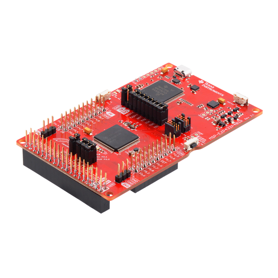
– MSP-EXP432P401R LaunchPad™
Development Kit
– MSP-TS432PZ100 100-Pin Target Board
– SimpleLink™ MSP432 Software Development
Kit (SDK)
• Operating Characteristics
– Wide Supply Voltage Range: 1.62 V to 3.7 V
– Temperature Range (Ambient): –40°C to 85°C
1
An IMPORTANT NOTICE at the end of this data sheet addresses availability, warranty, changes, use in safety-critical applications,
intellectual property matters and other important disclaimers. PRODUCTION DATA.
Product
Order
Folder
Now
®
-M4F CPU With Floating-
Tools and
Tools &
Technical
Software
Documents
SLAS826F – MARCH 2015 – REVISED MARCH 2017
• Flexible Clocking Features
– Tunable Internal DCO (up to 48 MHz)
– 32.768 kHz Low-Frequency Crystal Support
(LFXT)
– High-Frequency Crystal Support (HFXT) up to
48 MHz
– Low-Frequency Internal Reference Oscillator
(REFO)
– Very Low-Power Low-Frequency Internal
Oscillator (VLO)
– Module Oscillator (MODOSC)
– System Oscillator (SYSOSC)
• Code Security Features
– JTAG and SWD Lock
– IP Protection (up to Four Secure Flash Zones,
Each With Configurable Start Address and Size)
• Enhanced System Features
– Programmable Supervision and Monitoring of
Supply Voltage
– Multiple-Class Resets for Better Control of
Application and Debug
– 8-Channel DMA
– RTC With Calendar and Alarm Functions
• Timing and Control
– Up to Four 16-Bit Timers, Each With up to Five
Capture, Compare, PWM Capability
– Two 32-Bit Timers, Each With Interrupt
Generation Capability
• Serial Communication
– Up to Four eUSCI_A Modules
– UART With Automatic Baud-Rate Detection
– IrDA Encode and Decode
– SPI (up to 16 Mbps)
– Up to Four eUSCI_B Modules
2
– I
C (With Multiple-Slave Addressing)
– SPI (up to 16 Mbps)
• Flexible I/O Features
– Ultra-Low-Leakage I/Os (±20 nA Maximum)
– All I/Os With Capacitive-Touch Capability
– Up to 48 I/Os With Interrupt and Wake-up
Capability
– Up to 24 I/Os With Port Mapping Capability
– Eight I/Os With Glitch Filtering Capability
Support &
Community
MSP432P401R, MSP432P401M
Advertisement
Table of Contents

Related Manuals for Texas Instruments SimpleLink MSP432P401R


Summary of Contents for Texas Instruments SimpleLink MSP432P401R
-
Page 1: Device Overview
Support & Product Order Tools & Technical Community Folder Software Documents MSP432P401R, MSP432P401M SLAS826F – MARCH 2015 – REVISED MARCH 2017 MSP432P401R, MSP432P401M SimpleLink™ Mixed-Signal Microcontrollers 1 Device Overview Features • Core • Flexible Clocking Features ® ® – ARM 32-Bit Cortex -M4F CPU With Floating- –... -
Page 2: Applications
9, or see the website. (2) The sizes shown here are approximations. For the package dimensions with tolerances, see the Mechanical Data in Section Device Overview Copyright © 2015–2017, Texas Instruments Incorporated Submit Documentation Feedback Product Folder Links: MSP432P401R MSP432P401M... -
Page 3: Functional Block Diagram
5 CCR (I C, SPI) IrDA, SPI) Copyright © 2016, Texas Instruments Incorporated Figure 1-1. MSP432P401R, MSP432P401M Functional Block Diagram The CPU and all of the peripherals in the device interact with each other through a common AHB matrix. In some cases, there are bridges between the AHB ports and the peripherals. These bridges are transparent to the application from a memory map perspective and, therefore, are not shown in the block diagram. -
Page 4: Table Of Contents
5.17 Typical Characteristics of Low-Frequency Active Mechanical, Packaging, and Orderable ....Mode Currents for CoreMark Program ..........Information 5.18 Current Consumption in LDO-Based LPM0 Modes Table of Contents Copyright © 2015–2017, Texas Instruments Incorporated Submit Documentation Feedback Product Folder Links: MSP432P401R MSP432P401M... -
Page 5: Revision History
Updated Section 1.2, Applications ....................• Updated Section 1.3, Description ............ • Updated lists of software and tools in Section 8.3, Tools and Software Revision History Copyright © 2015–2017, Texas Instruments Incorporated Submit Documentation Feedback Product Folder Links: MSP432P401R MSP432P401M... -
Page 6: Device Comparison
3, 5 would represent two instantiations of Timer_A, the first instantiation having 3 and the second instantiation having 5 capture/compare registers and PWM output generators, respectively. Device Comparison Copyright © 2015–2017, Texas Instruments Incorporated Submit Documentation Feedback Product Folder Links:... -
Page 7: Related Products
TI Designs include schematic or block diagrams, BOMs, and design files to speed your time to market. Search and download designs at ti.com/tidesigns. Device Comparison Copyright © 2015–2017, Texas Instruments Incorporated Submit Documentation Feedback Product Folder Links: MSP432P401R MSP432P401M... -
Page 8: Terminal Configuration And Functions
SPI BSL pins: P1.4 - BSLSTE, P1.5 - BSLCLK, P1.6 - BSLSIMO, P1.7 - BSLSOMI C BSL pins: P3.6 - BSLSDA, P3.7 - BSLSCL Figure 4-1. 100-Pin PZ Package (Top View) Terminal Configuration and Functions Copyright © 2015–2017, Texas Instruments Incorporated Submit Documentation Feedback Product Folder Links: MSP432P401R MSP432P401M... - Page 9 SPI BSL pins: P1.4 - BSLSTE, P1.5 - BSLCLK, P1.6 - BSLSIMO, P1.7 - BSLSOMI C BSL pins: P3.6 - BSLSDA, P3.7 - BSLSCL Figure 4-2. 80-Pin ZXH Package (Top View) Terminal Configuration and Functions Copyright © 2015–2017, Texas Instruments Incorporated Submit Documentation Feedback Product Folder Links: MSP432P401R MSP432P401M...
- Page 10 SPI BSL pins: P1.4 - BSLSTE, P1.5 - BSLCLK, P1.6 - BSLSIMO, P1.7 - BSLSOMI C BSL pins: P3.6 - BSLSDA, P3.7 - BSLSCL Figure 4-3. 64-Pin RGC Package (Top View) Terminal Configuration and Functions Copyright © 2015–2017, Texas Instruments Incorporated Submit Documentation Feedback Product Folder Links: MSP432P401R MSP432P401M...
-
Page 11: Pin Attributes
OFF = High-impedance with Schmitt trigger and pullup or pulldown (if available) disabled PD = High-impedance input with pulldown enabled PU = High-impedance input with pullup enabled N/A = Not applicable Terminal Configuration and Functions Copyright © 2015–2017, Texas Instruments Incorporated Submit Documentation Feedback Product Folder Links: MSP432P401R MSP432P401M... - Page 12 LVCMOS DVCC TA2.0 LVCMOS DVCC C0.0 Analog DVCC P3.0 (RD) LVCMOS DVCC PM_UCA2STE LVCMOS DVCC P3.1 (RD) LVCMOS DVCC PM_UCA2CLK LVCMOS DVCC Terminal Configuration and Functions Copyright © 2015–2017, Texas Instruments Incorporated Submit Documentation Feedback Product Folder Links: MSP432P401R MSP432P401M...
- Page 13 LVCMOS DVCC Analog DVCC P9.1 (RD) LVCMOS DVCC Analog DVCC P6.0 (RD) LVCMOS DVCC Analog DVCC P6.1 (RD) LVCMOS DVCC Analog DVCC Terminal Configuration and Functions Copyright © 2015–2017, Texas Instruments Incorporated Submit Documentation Feedback Product Folder Links: MSP432P401R MSP432P401M...
- Page 14 P5.7 (RD) LVCMOS DVCC TA2.2 LVCMOS DVCC VREF- Analog DVCC VeREF- Analog DVCC C1.6 Analog DVCC DVSS2 – Power DVCC2 – Power Terminal Configuration and Functions Copyright © 2015–2017, Texas Instruments Incorporated Submit Documentation Feedback Product Folder Links: MSP432P401R MSP432P401M...
- Page 15 LVCMOS DVCC P7.1 (RD) LVCMOS DVCC PM_C0OUT LVCMOS DVCC PM_TA0CLK LVCMOS DVCC P7.2 (RD) LVCMOS DVCC PM_C1OUT LVCMOS DVCC PM_TA1CLK LVCMOS DVCC Terminal Configuration and Functions Copyright © 2015–2017, Texas Instruments Incorporated Submit Documentation Feedback Product Folder Links: MSP432P401R MSP432P401M...
- Page 16 P9.7 (RD) LVCMOS DVCC UCA3TXD LVCMOS DVCC UCA3SIMO LVCMOS DVCC P10.0 (RD) LVCMOS DVCC UCB3STE LVCMOS DVCC QFN Pad – – – Terminal Configuration and Functions Copyright © 2015–2017, Texas Instruments Incorporated Submit Documentation Feedback Product Folder Links: MSP432P401R MSP432P401M...
-
Page 17: Signal Descriptions
Output of low-frequency crystal oscillator LFXT MCLK MCLK clock output (1) N/A = not available (2) I = input, O = output Terminal Configuration and Functions Copyright © 2015–2017, Texas Instruments Incorporated Submit Documentation Feedback Product Folder Links: MSP432P401R MSP432P401M... - Page 18 General-purpose digital I/O with port interrupt and P1.6 wake-up capability General-purpose digital I/O with port interrupt and P1.7 wake-up capability Terminal Configuration and Functions Copyright © 2015–2017, Texas Instruments Incorporated Submit Documentation Feedback Product Folder Links: MSP432P401R MSP432P401M...
- Page 19 General-purpose digital I/O with port interrupt and P3.7 wake-up capability and with reconfigurable port mapping secondary function Terminal Configuration and Functions Copyright © 2015–2017, Texas Instruments Incorporated Submit Documentation Feedback Product Folder Links: MSP432P401R MSP432P401M...
- Page 20 General-purpose digital I/O with port interrupt, wake- P6.6 up, and glitch filtering capability General-purpose digital I/O with port interrupt, wake- P6.7 up, and glitch filtering capability Terminal Configuration and Functions Copyright © 2015–2017, Texas Instruments Incorporated Submit Documentation Feedback Product Folder Links: MSP432P401R MSP432P401M...
- Page 21 General-purpose digital I/O PJ.1 General-purpose digital I/O PJ.2 General-purpose digital I/O PJ.3 General-purpose digital I/O PJ.4 General-purpose digital I/O PJ.5 General-purpose digital I/O Terminal Configuration and Functions Copyright © 2015–2017, Texas Instruments Incorporated Submit Documentation Feedback Product Folder Links: MSP432P401R MSP432P401M...
- Page 22 C clock – eUSCI_B3 I C mode UCB3SDA C data – eUSCI_B3 I C mode UCB3SDA C data – eUSCI_B3 I C mode Terminal Configuration and Functions Copyright © 2015–2017, Texas Instruments Incorporated Submit Documentation Feedback Product Folder Links: MSP432P401R MSP432P401M...
- Page 23 PM_UCA2SOMI SPI mode Default mapping: Slave transmit enable – eUSCI_A2 PM_UCA2STE SPI mode Default mapping: Transmit data – eUSCI_A2 UART PM_UCA2TXD mode Terminal Configuration and Functions Copyright © 2015–2017, Texas Instruments Incorporated Submit Documentation Feedback Product Folder Links: MSP432P401R MSP432P401M...
- Page 24 (3) VCORE is for internal use only. No external current loading is possible. VCORE should only be connected to the recommended capacitor value, C VCORE Terminal Configuration and Functions Copyright © 2015–2017, Texas Instruments Incorporated Submit Documentation Feedback Product Folder Links: MSP432P401R MSP432P401M...
- Page 25 RSTn External reset (active low) SVMHOUT SVMH output QFN package exposed thermal pad. TI recommends Thermal QFN Pad – connection to VSS. Terminal Configuration and Functions Copyright © 2015–2017, Texas Instruments Incorporated Submit Documentation Feedback Product Folder Links: MSP432P401R MSP432P401M...
- Page 26 UCA0TXD Transmit data – eUSCI_A0 UART mode UART UCA3RXD Receive data – eUSCI_A3 UART mode UCA3TXD Transmit data – eUSCI_A3 UART mode Terminal Configuration and Functions Copyright © 2015–2017, Texas Instruments Incorporated Submit Documentation Feedback Product Folder Links: MSP432P401R MSP432P401M...
-
Page 27: Pin Multiplexing
(1) For any unused pin with a secondary function that is shared with general-purpose I/O, follow the guidelines for the Px.0 to Px.7 pins. Terminal Configuration and Functions Copyright © 2015–2017, Texas Instruments Incorporated Submit Documentation Feedback Product Folder Links:... -
Page 28: Specifications
(4) Does not include I/O currents (driven by application requirements). (5) Operating frequency may require the flash to be accessed with wait states. See Section 5.8 for further details. Specifications Copyright © 2015–2017, Texas Instruments Incorporated Submit Documentation Feedback Product Folder Links: MSP432P401R MSP432P401M... -
Page 29: Recommended External Components
MIN value, the DC-DC operation switches to LDO automatically, as long as the V drop is slower than the rate that is reliably detected. See Table 5-19 for more details. (4) Core voltage is off in LPM4.5 mode. Specifications Copyright © 2015–2017, Texas Instruments Incorporated Submit Documentation Feedback Product Folder Links: MSP432P401R MSP432P401M... -
Page 30: Operating Mode Cpu Frequency Ranges
Peripheral frequency in LPM3 mode for VCORE0 32.768 LPM3 and VCORE1 LPM3_VCORE1 LPM3.5 Peripheral frequency in LPM3.5 mode 32.768 LPM3.5 (1) Only RTC and WDT can be active. Specifications Copyright © 2015–2017, Texas Instruments Incorporated Submit Documentation Feedback Product Folder Links: MSP432P401R MSP432P401M... -
Page 31: Operating Mode Execution Frequency Vs Flash Wait-State Requirements
(8) Flash instruction and data buffers are enabled (BUFI = BUFD = 1). (9) Device executing the Dhrystone 2.1 program. Code execution from SRAM. Stack and data in SRAM. Specifications Copyright © 2015–2017, Texas Instruments Incorporated Submit Documentation Feedback Product Folder Links:... -
Page 32: Current Consumption In Dc-Dc-Based Active
(8) Flash instruction and data buffers are enabled (BUFI = BUFD = 1). (9) Device executing the Dhrystone 2.1 program. Code execution from SRAM. Stack and data in SRAM. Specifications Copyright © 2015–2017, Texas Instruments Incorporated Submit Documentation Feedback Product Folder Links:... -
Page 33: Typical Characteristics Of Active Mode Currents For Coremark Program
Flash Execution = 3 V = 25°C SRAM Execution = 3 V = 25°C Figure 5-3. Frequency vs Current Consumption Figure 5-4. Frequency vs Current Consumption Specifications Copyright © 2015–2017, Texas Instruments Incorporated Submit Documentation Feedback Product Folder Links: MSP432P401R MSP432P401M... -
Page 34: Typical Characteristics Of Active Mode Currents For Prime Number Program
Flash Execution = 3 V = 25°C SRAM Execution = 3 V = 25°C Figure 5-7. Frequency vs Current Consumption Figure 5-8. Frequency vs Current Consumption Specifications Copyright © 2015–2017, Texas Instruments Incorporated Submit Documentation Feedback Product Folder Links: MSP432P401R MSP432P401M... -
Page 35: Typical Characteristics Of Active Mode Currents For Fibonacci Program
Flash Execution = 3 V = 25°C SRAM Execution = 3 V = 25°C Figure 5-11. Frequency vs Current Consumption Figure 5-12. Frequency vs Current Consumption Specifications Copyright © 2015–2017, Texas Instruments Incorporated Submit Documentation Feedback Product Folder Links: MSP432P401R MSP432P401M... -
Page 36: Typical Characteristics Of Active Mode Currents For While(1) Program
Flash Execution = 3 V = 25°C SRAM Execution = 3 V = 25°C Figure 5-15. Frequency vs Current Consumption Figure 5-16. Frequency vs Current Consumption Specifications Copyright © 2015–2017, Texas Instruments Incorporated Submit Documentation Feedback Product Folder Links: MSP432P401R MSP432P401M... -
Page 37: Typical Characteristics Of Low-Frequency Active Mode Currents For Coremark Program
MCLK = 128 kHz SRAM Execution = 25°C MCLK = 128 kHz Figure 5-17. Supply Voltage vs Current Consumption Figure 5-18. Supply Voltage vs Current Consumption Specifications Copyright © 2015–2017, Texas Instruments Incorporated Submit Documentation Feedback Product Folder Links: MSP432P401R MSP432P401M... -
Page 38: Current Consumption In Ldo-Based Lpm0 Modes
(4) All peripherals are inactive. (5) Bank 0 of SRAM kept active. Rest of the banks are powered down. (6) CPU is off. Flash and SRAM not accessed. Specifications Copyright © 2015–2017, Texas Instruments Incorporated Submit Documentation Feedback Product Folder Links: MSP432P401R MSP432P401M... -
Page 39: Current Consumption In Lpm3, Lpm4 Modes
(6) WDT module is disabled. (7) SVSMH is disabled. (8) RTC sourced by REFO. (9) No core voltage. CPU, flash, and all banks of SRAM are powered down. Specifications Copyright © 2015–2017, Texas Instruments Incorporated Submit Documentation Feedback Product Folder Links: MSP432P401R MSP432P401M... -
Page 40: Current Consumption Of Digital Peripherals
(6) The junction-to-case (bottom) thermal resistance is obtained by simulating a cold plate test on the exposed (power) pad. No specific JEDEC standard test exists, but a close description can be found in the ANSI SEMI standard G30-88. Specifications Copyright © 2015–2017, Texas Instruments Incorporated Submit Documentation Feedback Product Folder Links:... -
Page 41: Timing And Switching Characteristics
LPMx.5_RSTn (1) External reset is applied on RSTn pin, and the latency is measured from release of external reset to start of user application code. Specifications Copyright © 2015–2017, Texas Instruments Incorporated Submit Documentation Feedback Product Folder Links: MSP432P401R MSP432P401M... - Page 42 SELM = 2, REFO frequency = 128 kHz Transition from AM_LF_VCORE1 to AM_LDO_VCORE1 AM_LF_VCORE1 AM_LDO_VCORE1 µs AMLF1_AMLDO1 SELM = 2, REFO frequency = 128 kHz Specifications Copyright © 2015–2017, Texas Instruments Incorporated Submit Documentation Feedback Product Folder Links: MSP432P401R MSP432P401M...
- Page 43 (1) This is the latency between execution of WFI instruction by CPU to assertion of SLEEPING signal at CPU output. (2) This is the latency between I/O interrupt event to deassertion of SLEEPING signal at CPU output. Specifications Copyright © 2015–2017, Texas Instruments Incorporated Submit Documentation Feedback Product Folder Links:...
- Page 44 (1) This is the latency from WFI instruction execution by CPU to LPM3 or LPM4 entry. (2) This is the latency from I/O wake-up event to MCLK clock start at device pin. Specifications Copyright © 2015–2017, Texas Instruments Incorporated Submit Documentation Feedback Product Folder Links:...
- Page 45 (2) This is the latency from WFI instruction execution by CPU to LPM4.5 mode entry. (3) This is the latency from I/O wake-up event to start of user application code. Specifications Copyright © 2015–2017, Texas Instruments Incorporated Submit Documentation Feedback Product Folder Links:...
- Page 46 For LFXTDRIVE = {2}, 6 pF ≤ C ≤ 10 pF. L,eff • For LFXTDRIVE = {3}, 6 pF ≤ C ≤ 12 pF. L,eff Specifications Copyright © 2015–2017, Texas Instruments Incorporated Submit Documentation Feedback Product Folder Links: MSP432P401R MSP432P401M...
- Page 47 HFXT from HFXT output to ground Crystal shunt capacitance = 1 MHz to 48 MHz SHUNT Crystal motional capacitance = 1 MHz to 48 MHz Specifications Copyright © 2015–2017, Texas Instruments Incorporated Submit Documentation Feedback Product Folder Links: MSP432P401R MSP432P401M...
- Page 48 (2) When HFXTBYPASS is set, HFXT circuits are automatically powered down. Input signal is a digital square wave with parametrics defined in the Schmitt-trigger Inputs section of this data sheet. Duty cycle requirements are defined by DC HFXT, SW Specifications Copyright © 2015–2017, Texas Instruments Incorporated Submit Documentation Feedback Product Folder Links: MSP432P401R MSP432P401M...
- Page 49 HFFREQ = 6, = 48 MHz, C = 16 pF HFXT,HF L,eff (3) Oscillation allowance is based on a safety factor of 5 for recommended crystals. Specifications Copyright © 2015–2017, Texas Instruments Incorporated Submit Documentation Feedback Product Folder Links: MSP432P401R MSP432P401M...
- Page 50 (7) Frequencies above the MAX specification do not set the fault flag. Frequencies in between the MIN and MAX might set the flag. A static condition or stuck at fault condition will set the flag. (8) Measured with logic-level input frequency but also applies to operation with crystals. Specifications Copyright © 2015–2017, Texas Instruments Incorporated Submit Documentation Feedback Product Folder Links: MSP432P401R MSP432P401M...
- Page 51 (3) Calculated using the box method: (MAX(1.62 V to 3.7 V) – MIN(1.62 V to 3.7 V)) / MIN(1.62 V to 3.7 V) / (3.7 V – 1.62 V) Specifications Copyright © 2015–2017, Texas Instruments Incorporated Submit Documentation Feedback Product Folder Links:...
- Page 52 1.62 V to 3.7 V ±0.2 ±0.7 ±1.2 External resistor 0°C 1.62 V to 3.7 V ±0.2 ±0.2 ±0.7 with 25-ppm TCR –40°C to 85 °C ±0.5 ±0.5 ±1 Specifications Copyright © 2015–2017, Texas Instruments Incorporated Submit Documentation Feedback Product Folder Links: MSP432P401R MSP432P401M...
- Page 53 (4) Calculated using the box method: (MAX(1.62 V to 3.7 V) – MIN(1.62 V to 3.7 V)) / MIN(1.62 V to 3.7 V) / (3.7 V – 1.62 V) Specifications Copyright © 2015–2017, Texas Instruments Incorporated Submit Documentation Feedback Product Folder Links:...
- Page 54 (3) Calculated using the box method: (MAX(1.62 V to 3.7 V) – MIN(1.62 V to 3.7 V)) / MIN(1.62 V to 3.7 V) / (3.7 V – 1.62 V) Specifications Copyright © 2015–2017, Texas Instruments Incorporated Submit Documentation Feedback Product Folder Links:...
- Page 55 Short circuit current limit for DC- Measured when output is shorted to SC-DCDC ground (1) When DV falls below this voltage, internally the regulator switches over to LDO from DC-DC. Specifications Copyright © 2015–2017, Texas Instruments Incorporated Submit Documentation Feedback Product Folder Links: MSP432P401R MSP432P401M...
- Page 56 SVSMHOFF = 0, SVSMHLP = 0, SVSMHTH = 6, 2.72 DC (dDV /dt < 1V/s) SVSMHOFF = 0, SVSMHLP = 0, SVSMHTH = 7, 2.92 3.01 3.12 DC (dDV /dt < 1V/s) Specifications Copyright © 2015–2017, Texas Instruments Incorporated Submit Documentation Feedback Product Folder Links: MSP432P401R MSP432P401M...
- Page 57 SVSMH module per the SVSMH on or off delay time specification. Otherwise, SVSMH may trip, causing the device to reset and wake up from the low-power mode. Specifications Copyright © 2015–2017, Texas Instruments Incorporated Submit Documentation Feedback Product Folder Links:...
- Page 58 The trigger pulse may or may not be filtered if the duration is between the MIN and MAX values. (5) Not applicable if RSTn/NMI pin configured as NMI. Specifications Copyright © 2015–2017, Texas Instruments Incorporated Submit Documentation Feedback Product Folder Links:...
- Page 59 (6) Measured between 20% of V to 80% of V (7) Measured between 80% of V to 20% of V Specifications Copyright © 2015–2017, Texas Instruments Incorporated Submit Documentation Feedback Product Folder Links: MSP432P401R MSP432P401M...
- Page 60 3.0 V 1150 (1) C is the external load capacitance connected from the output to VSS and includes all parasitic effects such as PCB traces. Specifications Copyright © 2015–2017, Texas Instruments Incorporated Submit Documentation Feedback Product Folder Links: MSP432P401R MSP432P401M...
- Page 61 = 2.2 V P7.0 = 3.0 V P7.0 Figure 5-21. High-Level Output Voltage vs Figure 5-22. High-Level Output Voltage vs High-Level Output Current High-Level Output Current Specifications Copyright © 2015–2017, Texas Instruments Incorporated Submit Documentation Feedback Product Folder Links: MSP432P401R MSP432P401M...
- Page 62 = 2.2 V P2.1 = 3.0 V P2.1 Figure 5-25. High-Level Output Voltage vs Figure 5-26. High-Level Output Voltage vs High-Level Output Current High-Level Output Current Specifications Copyright © 2015–2017, Texas Instruments Incorporated Submit Documentation Feedback Product Folder Links: MSP432P401R MSP432P401M...
- Page 63 One output active at a time = 2.2 V Figure 5-27. Load Capacitance vs Pin Oscillator Frequency Figure 5-28. Load Capacitance vs Pin Oscillator Frequency Specifications Copyright © 2015–2017, Texas Instruments Incorporated Submit Documentation Feedback Product Folder Links: MSP432P401R MSP432P401M...
- Page 64 (2) The internal reference supply current is not included in current consumption parameter I (ADC14) (3) Represents only the ADC switching capacitance. See the digital inputs electrical specification for internal parasitic pin capacitance. Specifications Copyright © 2015–2017, Texas Instruments Incorporated Submit Documentation Feedback Product Folder Links: MSP432P401R MSP432P401M...
- Page 65 (1) Minimum reference voltage of 1.45 V is necessary to meet the specified accuracy. Lower reference voltage down to 1.2 V can be applied for 1 Msps sampling rate with reduced accuracy requirements. (2) VeREF- pin should be connected to onboard ground for ADC14VRSEL = 0xE. Specifications Copyright © 2015–2017, Texas Instruments Incorporated Submit Documentation Feedback Product Folder Links: MSP432P401R MSP432P401M...
- Page 66 ADC14DIF = 1, ADC14VRSEL = 0xE (1) VeREF- pin should be connected to onboard ground for ADC14VRSEL = 0xE. (2) ADC clock derived from HFXT oscillator. Specifications Copyright © 2015–2017, Texas Instruments Incorporated Submit Documentation Feedback Product Folder Links: MSP432P401R MSP432P401M...
- Page 67 . No additional on time is needed. V1/2(on) V 1/2 (sample) Ambient Temperature (° C) D020 Figure 5-29. Typical Temperature Sensor Voltage Specifications Copyright © 2015–2017, Texas Instruments Incorporated Submit Documentation Feedback Product Folder Links: MSP432P401R MSP432P401M...
- Page 68 (2) Two decoupling capacitors, 5 µF and 50 nF, should be connected to VeREF+ terminal to decouple the dynamic current required for an external reference source if it is used for the ADC14. Also see the MSP432P4xx SimpleLink™ Microcontrollers Technical Reference Manual. Specifications Copyright © 2015–2017, Texas Instruments Incorporated Submit Documentation Feedback Product Folder Links: MSP432P401R MSP432P401M...
- Page 69 Sampling Rate (ksps) D054 VRSEL = 1 VREF = 2.5 V REFOUT = 1 ADC14PWRMD = 2 Resolution = 12 Bit Figure 5-34. Current vs Sampling Rate Specifications Copyright © 2015–2017, Texas Instruments Incorporated Submit Documentation Feedback Product Folder Links: MSP432P401R MSP432P401M...
- Page 70 VREF = 2.5 V Input Mode = Single Ended Input Mode = Differential Figure 5-39. INL vs ADC Output Code Figure 5-40. INL vs ADC Output Code Specifications Copyright © 2015–2017, Texas Instruments Incorporated Submit Documentation Feedback Product Folder Links: MSP432P401R MSP432P401M...
- Page 71 VREF = 2.5 V Input Mode = Single Ended Input Mode = Differential Figure 5-45. DNL vs ADC Output Code Figure 5-46. DNL vs ADC Output Code Specifications Copyright © 2015–2017, Texas Instruments Incorporated Submit Documentation Feedback Product Folder Links: MSP432P401R MSP432P401M...
- Page 72 Input Mode = Single Ended THD = -100 dB Input Mode = Differential Figure 5-51. Power vs Input Frequency Figure 5-52. Power vs Input Frequency Specifications Copyright © 2015–2017, Texas Instruments Incorporated Submit Documentation Feedback Product Folder Links: MSP432P401R MSP432P401M...
- Page 73 D076 = 20 kHz VRSEL = 14 = 20 kHz VRSEL = 14 Figure 5-55. THD vs Reference Voltage Figure 5-56. SFDR vs Reference Voltage Specifications Copyright © 2015–2017, Texas Instruments Incorporated Submit Documentation Feedback Product Folder Links: MSP432P401R MSP432P401M...
- Page 74 VRSEL = 14 VREF = 2.5 V = 20 kHz VRSEL = 14 VREF = 2.5 V Figure 5-59. THD vs Temperature Figure 5-60. SFDR vs Temperature Specifications Copyright © 2015–2017, Texas Instruments Incorporated Submit Documentation Feedback Product Folder Links: MSP432P401R MSP432P401M...
- Page 75 VRSEL = 14 VREF = 2.5 V Input Mode = Single Ended Input Mode = Differential Figure 5-63. DNL vs Temperature Figure 5-64. DNL vs Temperature Specifications Copyright © 2015–2017, Texas Instruments Incorporated Submit Documentation Feedback Product Folder Links: MSP432P401R MSP432P401M...
- Page 76 VREF = 2.5 V Input Mode = Single Ended Input Mode = Differential Figure 5-67. Gain Error vs Temperature Figure 5-68. Gain Error vs Temperature Specifications Copyright © 2015–2017, Texas Instruments Incorporated Submit Documentation Feedback Product Folder Links: MSP432P401R MSP432P401M...
- Page 77 (2) Calculated using the box method: (MAX(–40°C to 85°C) – MIN(–40°C to 85°C)) / MIN(–40°C to 85°C)/(85°C – (–40°C)). (3) The condition is that the error in a ADC conversion started after t is less than ±0.5 LSB. SETTLE Specifications Copyright © 2015–2017, Texas Instruments Incorporated Submit Documentation Feedback Product Folder Links: MSP432P401R MSP432P401M...
- Page 78 CEPWRMD = 00 or 01, CEF = 1, Overdrive ≥ 20 mV, CEFDLY = 10 CEPWRMD = 00 or 01, CEF = 1, Overdrive ≥ 20 mV, CEFDLY = 11 Specifications Copyright © 2015–2017, Texas Instruments Incorporated Submit Documentation Feedback Product Folder Links: MSP432P401R MSP432P401M...
- Page 79 VIN = reference into resistor ladder, (n + 0.9) (n + 1) (n + 1.1) CMP_REF a given tap n = 0 to 31 / 32 / 32 / 32 Specifications Copyright © 2015–2017, Texas Instruments Incorporated Submit Documentation Feedback Product Folder Links: MSP432P401R MSP432P401M...
- Page 80 Table 5-37. eUSCI (SPI Master Mode) Clock Frequency PARAMETER CONDITIONS MAX UNIT VCORE = 1.2 V SMCLK, eUSCI input clock frequency eUSCI Duty cycle = 50% ±10% VCORE = 1.4 V Specifications Copyright © 2015–2017, Texas Instruments Incorporated Submit Documentation Feedback Product Folder Links: MSP432P401R MSP432P401M...
- Page 81 SIMO output can become invalid before the output changing clock edge observed on UCLK. See the timing diagrams in Figure 5- Figure 5-70. Specifications Copyright © 2015–2017, Texas Instruments Incorporated Submit Documentation Feedback Product Folder Links: MSP432P401R MSP432P401M...
- Page 82 CKPL = 0 UCLK CKPL = 1 LOW/HIGH LOW/HIGH HD,MI SU,MI SOMI HD,MO VALID,MO STE,DIS STE,ACC SIMO Figure 5-70. SPI Master Mode, CKPH = 1 Specifications Copyright © 2015–2017, Texas Instruments Incorporated Submit Documentation Feedback Product Folder Links: MSP432P401R MSP432P401M...
- Page 83 CKPL = 0 UCLK CKPL = 1 SU,SI LOW/HIGH LOW/HIGH HD,SI SIMO HD,SO STE,ACC VALID,SO STE,DIS SOMI Figure 5-71. SPI Slave Mode, CKPH = 0 Specifications Copyright © 2015–2017, Texas Instruments Incorporated Submit Documentation Feedback Product Folder Links: MSP432P401R MSP432P401M...
- Page 84 CKPL = 0 UCLK CKPL = 1 LOW/HIGH LOW/HIGH HD,SI SU,SI SIMO HD,SO STE,ACC STE,DIS VALID,SO SOMI Figure 5-72. SPI Slave Mode, CKPH = 1 Specifications Copyright © 2015–2017, Texas Instruments Incorporated Submit Documentation Feedback Product Folder Links: MSP432P401R MSP432P401M...
- Page 85 UCCLTOx = 1 Clock low time-out UCCLTOx = 2 TIMEOUT UCCLTOx = 3 HD,STA SU,STA HD,STA HIGH SU,DAT SU,STO HD,DAT Figure 5-73. I C Mode Timing Specifications Copyright © 2015–2017, Texas Instruments Incorporated Submit Documentation Feedback Product Folder Links: MSP432P401R MSP432P401M...
- Page 86 (unless otherwise noted) PARAMETER TEST CONDITIONS UNIT CORE 1.2 V Timer32 operating clock frequency 1.4 V (1) Timer32 operates on the same clock as the Cortex-M4 CPU. Specifications Copyright © 2015–2017, Texas Instruments Incorporated Submit Documentation Feedback Product Folder Links: MSP432P401R MSP432P401M...
- Page 87 (3) The maximum value is theoretically calculated by multiplying the typical value by N for the specific erase or program endurance MAX_ERS and the total number of sectors in the flash main memory. Specifications Copyright © 2015–2017, Texas Instruments Incorporated Submit Documentation Feedback Product Folder Links: MSP432P401R MSP432P401M...
- Page 88 Time taken to enable all SRAM banks except Bank 0 µs SRAM_EN, all Time taken to disable all SRAM banks except Bank 0 µs SRAM_DIS, all Specifications Copyright © 2015–2017, Texas Instruments Incorporated Submit Documentation Feedback Product Folder Links: MSP432P401R MSP432P401M...
- Page 89 TDI_SU TDI_HLD TDI Input Valid TDI Input Valid TDO_ZDV TDO_DV TDO_DVZ TDO Output Valid TDO Output Valid Figure 5-75. JTAG Test Access Port (TAP) Timing Specifications Copyright © 2015–2017, Texas Instruments Incorporated Submit Documentation Feedback Product Folder Links: MSP432P401R MSP432P401M...
-
Page 90: Detailed Description
SWD and JTAG debug ports into one module, which allows a seamless switch between the 2-pin and 4-pin modes of operation, depending on application needs. Detailed Description Copyright © 2015–2017, Texas Instruments Incorporated Submit Documentation Feedback Product Folder Links:... -
Page 91: Memory Map
ROM, and the internal SRAM (permitting optimal single-cycle execution from the SRAM). Figure 6-2 shows the MSP432P401x-specific memory map of the Code zone, as visible to the user code. Detailed Description Copyright © 2015–2017, Texas Instruments Incorporated Submit Documentation Feedback Product Folder Links: MSP432P401R MSP432P401M... - Page 92 6.3.2 SRAM Zone Memory Map The SRAM zone of the device lies in the address range of 0x2000_0000 to 0x3FFF_FFFF. Figure 6-3 shows how this zone is divided. Detailed Description Copyright © 2015–2017, Texas Instruments Incorporated Submit Documentation Feedback Product Folder Links: MSP432P401R MSP432P401M...
- Page 93 The Peripheral zone of the device lies in the address range of 0x4000_0000 to 0x5FFF_FFFF. Figure 6-4 shows how this range is further divided. Detailed Description Copyright © 2015–2017, Texas Instruments Incorporated Submit Documentation Feedback Product Folder Links: MSP432P401R MSP432P401M...
- Page 94 0x4000_1800–0x4000_1BFF eUSCI_A2 Table 6-8 16-bit peripheral 0x4000_1C00–0x4000_1FFF eUSCI_A3 Table 6-9 16-bit peripheral 0x4000_2000–0x4000_23FF eUSCI_B0 Table 6-10 16-bit peripheral 0x4000_2400–0x4000_27FF eUSCI_B1 Table 6-11 16-bit peripheral Detailed Description Copyright © 2015–2017, Texas Instruments Incorporated Submit Documentation Feedback Product Folder Links: MSP432P401R MSP432P401M...
- Page 95 Timer_A0 Capture/Compare 1 TA0CCR1 Timer_A0 Capture/Compare 2 TA0CCR2 Timer_A0 Capture/Compare 3 TA0CCR3 Timer_A0 Capture/Compare 4 TA0CCR4 Timer_A0 Interrupt Vector TA0IV Timer_A0 Expansion 0 TA0EX0 Detailed Description Copyright © 2015–2017, Texas Instruments Incorporated Submit Documentation Feedback Product Folder Links: MSP432P401R MSP432P401M...
- Page 96 Timer_A3 Capture/Compare 0 TA3CCR0 Timer_A3 Capture/Compare 1 TA3CCR1 Timer_A3 Capture/Compare 2 TA3CCR2 Timer_A3 Capture/Compare 3 TA3CCR3 Timer_A3 Capture/Compare 4 TA3CCR4 Timer_A3 Interrupt Vector TA3IV Detailed Description Copyright © 2015–2017, Texas Instruments Incorporated Submit Documentation Feedback Product Folder Links: MSP432P401R MSP432P401M...
- Page 97 Transmit Buffer UCA2TXBUF eUSCI_A2 Auto Baud Rate Control UCA2ABCTL eUSCI_A2 IrDA Control UCA2IRCTL eUSCI_A2 Interrupt Enable UCA2IE eUSCI_A2 Interrupt Flag UCA2IFG eUSCI_A2 Interrupt Vector UCA2IV Detailed Description Copyright © 2015–2017, Texas Instruments Incorporated Submit Documentation Feedback Product Folder Links: MSP432P401R MSP432P401M...
- Page 98 I2C Own Address 0 UCB1I2COA0 eUSCI_B1 I2C Own Address 1 UCB1I2COA1 eUSCI_B1 I2C Own Address 2 UCB1I2COA2 eUSCI_B1 I2C Own Address 3 UCB1I2COA3 eUSCI_B1 Received Address UCB1ADDRX Detailed Description Copyright © 2015–2017, Texas Instruments Incorporated Submit Documentation Feedback Product Folder Links: MSP432P401R MSP432P401M...
- Page 99 Received Address UCB3ADDRX eUSCI_B3 Address Mask UCB3ADDMASK eUSCI_B3 I2C Slave Address UCB3I2CSA eUSCI_B3 Interrupt Enable UCB3IE eUSCI_B3 Interrupt Flag UCB3IFG eUSCI_B3 Interrupt Vector UCB3IV Detailed Description Copyright © 2015–2017, Texas Instruments Incorporated Submit Documentation Feedback Product Folder Links: MSP432P401R MSP432P401M...
- Page 100 CRC16 Data Input Low CRC16DI 010h CRC16 Data In Reverse Low CRC16DIRB 014h CRC16 Initialization and Result CRC16INIRES 018h CRC16 Result Reverse CRC16RESR 01Eh Detailed Description Copyright © 2015–2017, Texas Instruments Incorporated Submit Documentation Feedback Product Folder Links: MSP432P401R MSP432P401M...
- Page 101 01Bh Port 1 Interrupt Flag P1IFG 01Ch Port 2 Interrupt Flag P2IFG 01Dh Port 2 Interrupt Vector P2IV 01Eh Port 3 Input P3IN 020h Detailed Description Copyright © 2015–2017, Texas Instruments Incorporated Submit Documentation Feedback Product Folder Links: MSP432P401R MSP432P401M...
- Page 102 Port 6 Interrupt Vector P6IV 05Eh Port 7 Input P7IN 060h Port 8 Input P8IN 061h Port 7 Output P7OUT 062h Port 8 Output P8OUT 063h Detailed Description Copyright © 2015–2017, Texas Instruments Incorporated Submit Documentation Feedback Product Folder Links: MSP432P401R MSP432P401M...
- Page 103 Port J Resistor Enable PJREN 126h Port J Select 0 PJSEL0 12Ah Port J Select 1 PJSEL1 12Ch Port J Complement Select PJSELC 136h Detailed Description Copyright © 2015–2017, Texas Instruments Incorporated Submit Documentation Feedback Product Folder Links: MSP432P401R MSP432P401M...
- Page 104 Timer 1 Raw Interrupt Status T32RIS1 Timer 1 Interrupt Status T32MIS1 Timer 1 Background Load T32BGLOAD1 Timer 2 Load T32LOAD2 Timer 2 Current Value T32VALUE2 Detailed Description Copyright © 2015–2017, Texas Instruments Incorporated Submit Documentation Feedback Product Folder Links: MSP432P401R MSP432P401M...
- Page 105 104Ch Table 6-27. PCM Registers (Base Address: 0x4001_0000) REGISTER NAME ACRONYM OFFSET Control 0 PCMCTL0 Control 1 PCMCTL1 Interrupt Enable PCMIE Interrupt Flag PCMIFG Detailed Description Copyright © 2015–2017, Texas Instruments Incorporated Submit Documentation Feedback Product Folder Links: MSP432P401R MSP432P401M...
- Page 106 Program Burst Data0 3 FLCTL_PRGBRST_DATA0_3 06Ch Program Burst Data1 0 FLCTL_PRGBRST_DATA1_0 070h Program Burst Data1 1 FLCTL_PRGBRST_DATA1_1 074h Program Burst Data1 2 FLCTL_PRGBRST_DATA1_2 078h Detailed Description Copyright © 2015–2017, Texas Instruments Incorporated Submit Documentation Feedback Product Folder Links: MSP432P401R MSP432P401M...
- Page 107 Memory Control 1 ADC14MCTL1 Memory Control 2 ADC14MCTL2 Memory Control 3 ADC14MCTL3 Memory Control 4 ADC14MCTL4 Memory Control 5 ADC14MCTL5 Memory Control 6 ADC14MCTL6 Detailed Description Copyright © 2015–2017, Texas Instruments Incorporated Submit Documentation Feedback Product Folder Links: MSP432P401R MSP432P401M...
- Page 108 Memory 14 ADC14MEM14 Memory 15 ADC14MEM15 Memory 16 ADC14MEM16 Memory 17 ADC14MEM17 Memory 18 ADC14MEM18 Memory 19 ADC14MEM19 Memory 20 ADC14MEM20 Memory 21 ADC14MEM21 Detailed Description Copyright © 2015–2017, Texas Instruments Incorporated Submit Documentation Feedback Product Folder Links: MSP432P401R MSP432P401M...
- Page 109 In other words, writes to the bit-band alias region for these peripherals must be in the form of byte or half-word accesses only. Detailed Description Copyright © 2015–2017, Texas Instruments Incorporated Submit Documentation Feedback Product Folder Links: MSP432P401R MSP432P401M...
- Page 110 RSTCTL_PSSRESET_STAT 100h PSS Reset Status Clear RSTCTL_PSSRESET_CLR 104h PCM Reset Status RSTCTL_PCMRESET_STAT 108h PCM Reset Status Clear RSTCTL_PCMRESET_CLR 10Ch Pin Reset Status RSTCTL_PINRESET_STAT 110h Detailed Description Copyright © 2015–2017, Texas Instruments Incorporated Submit Documentation Feedback Product Folder Links: MSP432P401R MSP432P401M...
-
Page 111: Memories On The Msp432P401X
Figure 6-5 shows the memory map of the flash on MSP432P401x MCUs. Detailed Description Copyright © 2015–2017, Texas Instruments Incorporated Submit Documentation Feedback Product Folder Links: MSP432P401R MSP432P401M... - Page 112 In low-power modes of operation, the flash memory is disabled and put in a power-down state to minimize leakage. Detailed Description Copyright © 2015–2017, Texas Instruments Incorporated Submit Documentation Feedback Product Folder Links: MSP432P401R MSP432P401M...
- Page 113 The application can also disable one (or more) banks for a certain stage in the processing and enable it for another stage. Detailed Description Copyright © 2015–2017, Texas Instruments Incorporated Submit Documentation Feedback Product Folder Links:...
-
Page 114: Dma
(described in Section 6.5.2). For details regarding configuration of the DMA, see the DMA chapter in the MSP432P4xx SimpleLink™ Microcontrollers Technical Reference Manual. Detailed Description Copyright © 2015–2017, Texas Instruments Incorporated Submit Documentation Feedback Product Folder Links: MSP432P401R MSP432P401M... -
Page 115: Memory Map Access Details
ICODE: Cortex-M4 instruction fetch bus. Accesses the Code zone only • DCODE: Cortex-M4 data and literal load/store bus. Accesses the Code zone only. Debugger accesses to Code zone also appear on this bus. Detailed Description Copyright © 2015–2017, Texas Instruments Incorporated Submit Documentation Feedback Product Folder Links: MSP432P401R MSP432P401M... - Page 116 (3) Writes to this address are ignored if the sector has write protection enabled. (4) Reads from the bit-band region return 00h if the bit is clear and 01h if the bit is set. Detailed Description Copyright © 2015–2017, Texas Instruments Incorporated Submit Documentation Feedback Product Folder Links:...
-
Page 117: Interrupts
INTISR[0] INTISR[1] (1) This source can also be mapped to the system NMI. See the MSP432P4xx SimpleLink™ Microcontrollers Technical Reference Manual for more details. Detailed Description Copyright © 2015–2017, Texas Instruments Incorporated Submit Documentation Feedback Product Folder Links: MSP432P401R MSP432P401M... - Page 118 FPSCR. (3) DMA_INT0 has a different functionality from DMA_INT1, DMA_INT2, or DMA_INT3. See Section 6.5.2 for more details. Detailed Description Copyright © 2015–2017, Texas Instruments Incorporated Submit Documentation Feedback Product Folder Links: MSP432P401R MSP432P401M...
-
Page 119: System Control
Depending on the source of the reset, the device may exhibit different wake-up latencies from the POR. This implementation enables optimization of the reset recovery time. Detailed Description Copyright © 2015–2017, Texas Instruments Incorporated Submit Documentation Feedback Product Folder Links:... - Page 120 PCM can extend the reset to allow the system to settle before releasing the Reset. This reduces the chance of nondeterministic behavior. Detailed Description Copyright © 2015–2017, Texas Instruments Incorporated Submit Documentation Feedback Product Folder Links: MSP432P401R MSP432P401M...
- Page 121 VCCDET trip points, it generates a brownout condition, thereby initiating a device reset (POR class reset). Detailed Description Copyright © 2015–2017, Texas Instruments Incorporated Submit Documentation Feedback Product Folder Links:...
- Page 122 LDO based low-power mode, core voltage level 0, no retention of peripheral registers, RTC and WDT can be LPM3.5 active LPM4.5 Core voltage turned off, wake-up only through pin reset or wake-up capable I/Os Detailed Description Copyright © 2015–2017, Texas Instruments Incorporated Submit Documentation Feedback Product Folder Links: MSP432P401R MSP432P401M...
- Page 123 Fail-Safe Clock LFXT oscillator fault REFO clock HFXT oscillator fault SYSOSC clock DCO external resistor open circuit fault DCO clock in internal resistor mode Detailed Description Copyright © 2015–2017, Texas Instruments Incorporated Submit Documentation Feedback Product Folder Links: MSP432P401R MSP432P401M...
-
Page 124: Peripherals
NOTE The glitch filter is implemented on the following digital I/Os on MSP432P401x MCUs: P1.0, P1.4, P1.5, P3.0, P3.4, P3.5, P6.6, and P6.7. Detailed Description Copyright © 2015–2017, Texas Instruments Incorporated Submit Documentation Feedback Product Folder Links: MSP432P401R MSP432P401M... - Page 125 TA1 CCR2 compare output Out2 PM_TA1.3 TA1 CCR3 capture input CCI3A TA1 CCR3 compare output Out3 PM_TA1.4 TA1 CCR4 capture input CCI4A TA1 CCR4 compare output Out4 Detailed Description Copyright © 2015–2017, Texas Instruments Incorporated Submit Documentation Feedback Product Folder Links: MSP432P401R MSP432P401M...
- Page 126 TA1 CCR2 compare output Out2 P7.7/PM_TA1.1/C0.2 PM_TA1.1 TA1 CCR1 capture input CCI1A TA1 CCR1 compare output Out1 (1) Not available on the 64-pin RGC package. Detailed Description Copyright © 2015–2017, Texas Instruments Incorporated Submit Documentation Feedback Product Folder Links: MSP432P401R MSP432P401M...
- Page 127 Internal signals that are sourced by the Timer outputs may connect to other modules (for example, other timers or the ADC) in the device (as trigger sources). Detailed Description Copyright © 2015–2017, Texas Instruments Incorporated Submit Documentation Feedback Product Folder Links:...
- Page 128 CCR2 ADC14 (internal) ADC14SHSx = {2} P2.6/PM_TA0.3 CCI3A C1OUT (internal) CCI3B P2.6/PM_TA0.3 CCR3 TA0_C3 (internal) P2.7/PM_TA0.4 CCI4A TA1_C4 (Internal) CCI4B P2.7/PM_TA0.4 CCR4 TA0_C4 (internal) Detailed Description Copyright © 2015–2017, Texas Instruments Incorporated Submit Documentation Feedback Product Folder Links: MSP432P401R MSP432P401M...
- Page 129 CCR2 ADC14 (internal) ADC14SHSx = {4} P7.5/PM_TA1.3/C0.4 CCI3A C1OUT (internal) CCI3B P7.5/PM_TA1.3/C0.4 CCR3 TA1_C3 (internal) P7.4/PM_TA1.4/C0.5 CCI4A TA0_C4 (internal) CCI4B P7.4/PM_TA1.4/C0.5 CCR4 TA1_C4 (internal) Detailed Description Copyright © 2015–2017, Texas Instruments Incorporated Submit Documentation Feedback Product Folder Links: MSP432P401R MSP432P401M...
- Page 130 P6.6/TA2.3/UCB3SIMO/UCB3SDA/C CCI3A P6.6/TA2.3/UCB3SIMO/ TA3_C3 (internal) CCI3B CCR3 UCB3SDA/C1.1 TA2_C3 (internal) P6.7/TA2.4/UCB3SOMI/UCB3SCL/C CCI4A P6.7/TA2.4/UCB3SOMI/ From Capacitive Touch I/O 0 CCI4B CCR4 UCB3SCL/C1.0 (internal) TA2_C4 (internal) Detailed Description Copyright © 2015–2017, Texas Instruments Incorporated Submit Documentation Feedback Product Folder Links: MSP432P401R MSP432P401M...
- Page 131 31 days and includes leap year correction. The RTC_C also supports flexible alarm functions, offset calibration, and temperature compensation. The RTC_C operation is available in LPM3 and LPM3.5 modes to minimize power consumption. Detailed Description Copyright © 2015–2017, Texas Instruments Incorporated Submit Documentation Feedback Product Folder Links: MSP432P401R MSP432P401M...
- Page 132 The window comparators with a lower and upper limit allow CPU independent result monitoring through different window comparator interrupt flags. Detailed Description Copyright © 2015–2017, Texas Instruments Incorporated Submit Documentation Feedback Product Folder Links:...
- Page 133 (2) See the ADC14 chapter in the MSP432P4xx SimpleLink™ Microcontrollers Technical Reference Manual for details on the registers that contain the control bits listed in the table. Detailed Description Copyright © 2015–2017, Texas Instruments Incorporated Submit Documentation Feedback Product Folder Links: MSP432P401R MSP432P401M...
-
Page 134: Code Development And Debug
In low-power modes, the user can enable the debugger to override the state of the PSS, thereby gaining access to debug and trace features. Detailed Description Copyright © 2015–2017, Texas Instruments Incorporated Submit Documentation Feedback Product Folder Links:... - Page 135 POR reset event with the configured pin. For the complete description of the BSL features and its implementation, see the MSP432P401R Bootloader (BSL) User's Guide. Detailed Description Copyright © 2015–2017, Texas Instruments Incorporated Submit Documentation Feedback Product Folder Links: MSP432P401R MSP432P401M...
-
Page 136: Performance Benchmarks
Active Mode Voltage Integrity 1.62 V Inactive Power Mode Name LPM3 Inactive Clock Configuration CPU: OFF, RTC: 32 kHz Inactive Mode Voltage Integrity 1.62 V Detailed Description Copyright © 2015–2017, Texas Instruments Incorporated Submit Documentation Feedback Product Folder Links: MSP432P401R MSP432P401M... - Page 137 Table 6-61. Profile Configuration CONFIGURATION DETAILS Active Power Mode Name Active Mode Active Mode Clock Configuration CPU: 3 MHz Active Mode Voltage Integrity 1.62 V Detailed Description Copyright © 2015–2017, Texas Instruments Incorporated Submit Documentation Feedback Product Folder Links: MSP432P401R MSP432P401M...
-
Page 138: Input/Output Diagrams
DVCC 0: Input 1: Output PyOUT.x From module DVSS Py.x/USCI DVSS PySEL1.x PySEL0.x PyIN.x To module Functional representation only. Figure 6-7. Py.x/USCI Pin Diagram Detailed Description Copyright © 2015–2017, Texas Instruments Incorporated Submit Documentation Feedback Product Folder Links: MSP432P401R MSP432P401M... - Page 139 I: 0; O: 1 UCB0SIMO/UCB0SDA P1.6/UCB0SIMO/UCB0SDA DVSS DVSS (1) X = don't care (2) Direction controlled by eUSCI_A0 module. (3) Direction controlled by eUSCI_B0 module. Detailed Description Copyright © 2015–2017, Texas Instruments Incorporated Submit Documentation Feedback Product Folder Links: MSP432P401R MSP432P401M...
- Page 140 Table 6-62. Port P1 (P1.0 to P1.7) Pin Functions (continued) CONTROL BITS OR SIGNALS PIN NAME (P1.x) FUNCTION P1DIR.x P1SEL1.x P1SEL0.x P1.7 (I/O) I: 0; O: 1 UCB0SOMI/UCB0SCL P1.7/UCB0SOMI/UCB0SCL DVSS DVSS Detailed Description Copyright © 2015–2017, Texas Instruments Incorporated Submit Documentation Feedback Product Folder Links: MSP432P401R MSP432P401M...
- Page 141 DVSS P2.3 (I/O) I: 0; O: 1 UCA1TXD/UCA1SIMO default P2.3/PM_UCA1TXD/PM_U CA1SIMO DVSS DVSS (1) X = don't care (2) Direction controlled by eUSCI_A1 module. Detailed Description Copyright © 2015–2017, Texas Instruments Incorporated Submit Documentation Feedback Product Folder Links: MSP432P401R MSP432P401M...
- Page 142 I: 0; O: 1 UCB2CLK default P3.5/PM_UCB2CLK DVSS DVSS (1) X = don't care (2) Direction controlled by eUSCI_A2 module. (3) Direction controlled by eUSCI_B2 module. Detailed Description Copyright © 2015–2017, Texas Instruments Incorporated Submit Documentation Feedback Product Folder Links: MSP432P401R MSP432P401M...
- Page 143 P3.6 (I/O) I: 0; O: 1 UCB2SIMO/UCB2SDA default P3.6/PM_UCB2SIMO/PM_ UCB2SDA DVSS DVSS P3.7 (I/O) I: 0; O: 1 UCB2SOMI/UCB2SCL default P3.7/PM_UCB2SOMI/PM_ UCB2SCL DVSS DVSS Detailed Description Copyright © 2015–2017, Texas Instruments Incorporated Submit Documentation Feedback Product Folder Links: MSP432P401R MSP432P401M...
- Page 144 I: 0; O: 1 UCA3TXD/UCA3SIMO P9.7/UCA3TXD/UCA3SIMO DVSS DVSS (1) X = don't care (2) Not available on 80ZXH and 64RGC packages. (3) Direction controlled by eUSCI_A3 module. Detailed Description Copyright © 2015–2017, Texas Instruments Incorporated Submit Documentation Feedback Product Folder Links: MSP432P401R MSP432P401M...
- Page 145 I: 0; O: 1 UCB3SOMI/UCB3SCL P10.3/UCB3SOMI/UCB3SCL DVSS DVSS (1) X = don't care (2) Not available on 80ZXH and 64RGC packages. (3) Direction controlled by eUSCI_B3 module. Detailed Description Copyright © 2015–2017, Texas Instruments Incorporated Submit Documentation Feedback Product Folder Links: MSP432P401R MSP432P401M...
- Page 146 DVCC 0: Input 1: Output PyOUT.x From module DVSS Py.x/Mod1/Mod2 DVSS PySEL1.x PySEL0.x PyIN.x To module Functional representation only. Figure 6-8. Py.x/Mod1/Mod2 Pin Diagram Detailed Description Copyright © 2015–2017, Texas Instruments Incorporated Submit Documentation Feedback Product Folder Links: MSP432P401R MSP432P401M...
- Page 147 P2.7 (I/O) I: 0; O: 1 TA0.CCI4A default TA0.4 P2.7/PM_TA0.4 DVSS DVSS (1) X = don't care (2) Not available on the 64-pin RGC package. Detailed Description Copyright © 2015–2017, Texas Instruments Incorporated Submit Documentation Feedback Product Folder Links: MSP432P401R MSP432P401M...
- Page 148 TA1CLK default C1OUT P7.2/PM_C1OUT/ PM_TA1CLK DVSS DVSS P7.3 (I/O) I: 0; O: 1 TA0.CCI0A default TA0.0 P7.3/PM_TA0.0 DVSS DVSS (1) X = don't care Detailed Description Copyright © 2015–2017, Texas Instruments Incorporated Submit Documentation Feedback Product Folder Links: MSP432P401R MSP432P401M...
- Page 149 TA3.CCI3A TA3.3 P9.2/TA3.3 DVSS DVSS P9.3 (I/O) I: 0; O: 1 TA3.CCI4A TA3.4 P9.3/TA3.4 DVSS DVSS (1) Not available on 80ZXH and 64RGC packages. Detailed Description Copyright © 2015–2017, Texas Instruments Incorporated Submit Documentation Feedback Product Folder Links: MSP432P401R MSP432P401M...
- Page 150 Note: Output is DVSS if module 1 or module 2 function is not available. See the pin function tables. Functional representation only. Figure 6-9. Py.x/Mod1/Mod2/Az Pin Diagram Detailed Description Copyright © 2015–2017, Texas Instruments Incorporated Submit Documentation Feedback Product Folder Links: MSP432P401R MSP432P401M...
- Page 151 (2) Not available on the 64-pin RGC package. (3) Setting P4SEL1.x and P4SEL0.x disables the output driver and the input Schmitt trigger to prevent parasitic cross currents when applying analog signals. Detailed Description Copyright © 2015–2017, Texas Instruments Incorporated Submit Documentation Feedback Product Folder Links: MSP432P401R MSP432P401M...
- Page 152 Table 6-70. Port P4 (P4.0 to P4.7) Pin Functions (continued) CONTROL BITS OR SIGNALS PIN NAME (P4.x) FUNCTION P4DIR.x P4SEL1.x P4SEL0.x P4.7 (I/O) I: 0; O: 1 DVSS P4.7/A6 DVSS Detailed Description Copyright © 2015–2017, Texas Instruments Incorporated Submit Documentation Feedback Product Folder Links: MSP432P401R MSP432P401M...
- Page 153 (1) X = don't care (2) Setting P5SEL1.x and P5SEL0.x disables the output driver and the input Schmitt trigger to prevent parasitic cross currents when applying analog signals. Detailed Description Copyright © 2015–2017, Texas Instruments Incorporated Submit Documentation Feedback Product Folder Links: MSP432P401R MSP432P401M...
- Page 154 (2) Not available on the 64-pin RGC package. (3) Setting P6SEL1.x and P6SEL0.x disables the output driver and the input Schmitt trigger to prevent parasitic cross currents when applying analog signals. Detailed Description Copyright © 2015–2017, Texas Instruments Incorporated Submit Documentation Feedback Product Folder Links: MSP432P401R MSP432P401M...
- Page 155 (2) Not available on 80ZXH and 64RGC packages. (3) Setting P8SEL1.x and P8SEL0.x disables the output driver and the input Schmitt trigger to prevent parasitic cross currents when applying analog signals. Detailed Description Copyright © 2015–2017, Texas Instruments Incorporated Submit Documentation Feedback Product Folder Links: MSP432P401R MSP432P401M...
- Page 156 (2) Not available on 80ZXH and 64RGC packages. (3) Setting P9SEL1.x and P9SEL0.x disables the output driver and the input Schmitt trigger to prevent parasitic cross currents when applying analog signals. Detailed Description Copyright © 2015–2017, Texas Instruments Incorporated Submit Documentation Feedback Product Folder Links: MSP432P401R MSP432P401M...
- Page 157 0: Input 1: Output PyOUT.x From module DVSS Py.x/Mod/VREF/VeREF/Cp.q DVSS PySEL1.x PySEL0.x PyIN.x Keeper To module Functional representation only. Figure 6-10. Py.x/Mod/VREF/VeREF/Cp.q Pin Diagram Detailed Description Copyright © 2015–2017, Texas Instruments Incorporated Submit Documentation Feedback Product Folder Links: MSP432P401R MSP432P401M...
- Page 158 Selecting the C1.q input pin to the comparator multiplexer with the CEIPSEL or CEIMSEL bits automatically disables the output driver and input buffer for that pin, regardless of the state of the associated CEPD.q bit. Detailed Description Copyright © 2015–2017, Texas Instruments Incorporated Submit Documentation Feedback Product Folder Links:...
- Page 159 0: Input 1: Output PyOUT.x From module DVSS DVSS Py.x/USCI/Cp.q PySEL1.x PySEL0.x PyIN.x Keeper To module Functional representation only. Figure 6-11. Py.x/USCI/Cp.q Pin Diagram Detailed Description Copyright © 2015–2017, Texas Instruments Incorporated Submit Documentation Feedback Product Folder Links: MSP432P401R MSP432P401M...
- Page 160 Selecting the C1.q input pin to the comparator multiplexer with the CEIPSEL or CEIMSEL bits automatically disables the output driver and input buffer for that pin, regardless of the state of the associated CEPD.q bit. Detailed Description Copyright © 2015–2017, Texas Instruments Incorporated Submit Documentation Feedback Product Folder Links:...
- Page 161 0: Input 1: Output PyOUT.x From module From USCI DVSS Py.x/Mod/USCI/Cp.q PySEL1.x PySEL0.x PyIN.x Keeper To modules Functional representation only. Figure 6-12. Py.x/Mod/USCI/Cp.q Pin Diagram Detailed Description Copyright © 2015–2017, Texas Instruments Incorporated Submit Documentation Feedback Product Folder Links: MSP432P401R MSP432P401M...
- Page 162 Selecting the C1.q input pin to the comparator multiplexer with the CEIPSEL or CEIMSEL bits automatically disables the output driver and input buffer for that pin, regardless of the state of the associated CEPD.q bit. Detailed Description Copyright © 2015–2017, Texas Instruments Incorporated Submit Documentation Feedback Product Folder Links:...
- Page 163 0: Input 1: Output PyOUT.x From USCI From module DVSS Py.x/USCI/Mod/Cp.q PySEL1.x PySEL0.x PyIN.x Keeper To modules Functional representation only. Figure 6-13. Py.x/USCI/Mod/Cp.q Pin Diagram Detailed Description Copyright © 2015–2017, Texas Instruments Incorporated Submit Documentation Feedback Product Folder Links: MSP432P401R MSP432P401M...
- Page 164 Selecting the C0.q input pin to the comparator multiplexer with the CEIPSEL or CEIMSEL bits automatically disables the output driver and input buffer for that pin, regardless of the state of the associated CEPD.q bit. Detailed Description Copyright © 2015–2017, Texas Instruments Incorporated Submit Documentation Feedback Product Folder Links:...
- Page 165 0: Input 1: Output PyOUT.x From module DVSS Py.x/Mod/Cp.q DVSS PySEL1.x PySEL0.x PyIN.x Keeper To module Functional representation only. Figure 6-14. Py.x/Mod/Cp.q Pin Diagram Detailed Description Copyright © 2015–2017, Texas Instruments Incorporated Submit Documentation Feedback Product Folder Links: MSP432P401R MSP432P401M...
- Page 166 Selecting the C0.q input pin to the comparator multiplexer with the CEIPSEL or CEIMSEL bits automatically disables the output driver and input buffer for that pin, regardless of the state of the associated CEPD.q bit. Detailed Description Copyright © 2015–2017, Texas Instruments Incorporated Submit Documentation Feedback Product Folder Links:...
- Page 167 0: Input 1: Output PyOUT.x From module DVSS Py.x/Mod/Cp.q DVSS PySEL1.x PySEL0.x PyIN.x Keeper To module Functional representation only. Figure 6-15. Py.x/Mod/Cp.q Pin Diagram Detailed Description Copyright © 2015–2017, Texas Instruments Incorporated Submit Documentation Feedback Product Folder Links: MSP432P401R MSP432P401M...
- Page 168 Selecting the C0.q input pin to the comparator multiplexer with the CEIPSEL or CEIMSEL bits automatically disables the output driver and input buffer for that pin, regardless of the state of the associated CEPD.q bit. Detailed Description Copyright © 2015–2017, Texas Instruments Incorporated Submit Documentation Feedback Product Folder Links:...
- Page 169 0: Input 1: Output PJOUT.0 DVSS DVSS PJ.0/LFXIN DVSS PJSEL0.0 PJSEL1.0 PJIN.0 Keeper To modules Functional representation only. Figure 6-16. Port PJ (PJ.0) Diagram Detailed Description Copyright © 2015–2017, Texas Instruments Incorporated Submit Documentation Feedback Product Folder Links: MSP432P401R MSP432P401M...
- Page 170 0: Input 1: Output PJOUT.1 DVSS DVSS PJ.1/LFXOUT DVSS PJSEL0.1 PJSEL1.1 PJIN.1 Keeper To modules Functional representation only. Figure 6-17. Port PJ (PJ.1) Diagram Detailed Description Copyright © 2015–2017, Texas Instruments Incorporated Submit Documentation Feedback Product Folder Links: MSP432P401R MSP432P401M...
- Page 171 (4) With PJSEL0.1 = 1 or PJSEL1.1 =1 the general-purpose I/O functionality is disabled. No input function is available. When configured as output, the pin is actively pulled to zero. Detailed Description Copyright © 2015–2017, Texas Instruments Incorporated Submit Documentation Feedback Product Folder Links:...
- Page 172 0: Input 1: Output PJOUT.3 DVSS DVSS PJ.3/HFXIN DVSS PJSEL0.3 PJSEL1.3 PJIN.3 Keeper To modules Functional representation only. Figure 6-18. Port PJ (PJ.2) Diagram Detailed Description Copyright © 2015–2017, Texas Instruments Incorporated Submit Documentation Feedback Product Folder Links: MSP432P401R MSP432P401M...
- Page 173 0: Input 1: Output PJOUT.2 DVSS DVSS PJ.2/HFXOUT DVSS PJSEL0.2 PJSEL1.2 PJIN.2 Keeper To modules Functional representation only. Figure 6-19. Port PJ (PJ.3) Diagram Detailed Description Copyright © 2015–2017, Texas Instruments Incorporated Submit Documentation Feedback Product Folder Links: MSP432P401R MSP432P401M...
- Page 174 (4) With PJSEL0.2 = 1 or PJSEL1.2 =1 the general-purpose I/O functionality is disabled. No input function is available. When configured as output, the pin is actively pulled to zero. Detailed Description Copyright © 2015–2017, Texas Instruments Incorporated Submit Documentation Feedback Product Folder Links:...
- Page 175 JTAG (4 wire) SWDIOTMS SWDIO (I/O) SWD (2 wire) (1) This pin is internally pulled to DV (2) This pin is internal pulled to DV Detailed Description Copyright © 2015–2017, Texas Instruments Incorporated Submit Documentation Feedback Product Folder Links: MSP432P401R MSP432P401M...
-
Page 176: Device Descriptors (Tlv)
DCO ER Mode: DCO Constant (K) for DCORSEL 5 00201088h per unit (1) per unit = content can differ from device to device Detailed Description Copyright © 2015–2017, Texas Instruments Incorporated Submit Documentation Feedback Product Folder Links: MSP432P401R MSP432P401M... - Page 177 TLV End Word 00201148h 0BD0E11Dh Reserved 0020114Ch-00201FFFh FFFFFFFFh (2) 128-Bit Random Number: The random number is generated during production test using the CryptGenRandom() function from Microsoft®. Detailed Description Copyright © 2015–2017, Texas Instruments Incorporated Submit Documentation Feedback Product Folder Links: MSP432P401R MSP432P401M...
-
Page 178: Identification
1. Version: IEEE 1149.1 defines a 4 bit field where as the Coresight compliant PID registers have 4 bits each for Revision (major revision) and RevAnd (minor revision) Detailed Description Copyright © 2015–2017, Texas Instruments Incorporated Submit Documentation Feedback Product Folder Links:... - Page 179 As an example, the ROM table with IEEE 1149.1-complaint device IDCODE for the MSP432P401xx MCU is 0000-1011-1001-1010-1111-0000-0010-1111 (see Figure 6-21). Figure 6-21. Example of ROM PID Entries for MSP432P401xx MCU Detailed Description Copyright © 2015–2017, Texas Instruments Incorporated Submit Documentation Feedback Product Folder Links: MSP432P401R MSP432P401M...
-
Page 180: Applications, Implementation, And Layout
In this case, the associated LFXOUT and HFXOUT pins can be used for other purposes. Figure 7-2 shows a typical connection diagram. LFXIN LFXOUT HFXIN HFXOUT Figure 7-2. Typical Crystal Connection Applications, Implementation, and Layout Copyright © 2015–2017, Texas Instruments Incorporated Submit Documentation Feedback Product Folder Links: MSP432P401R MSP432P401M... -
Page 181: Peripheral And Interface-Specific Design Information
ADC. The general guidelines in Section 7.1.1 combined with the connections shown in Section 7.2.1.1 prevent this. Applications, Implementation, and Layout Copyright © 2015–2017, Texas Instruments Incorporated Submit Documentation Feedback Product Folder Links: MSP432P401R MSP432P401M... - Page 182 If differential mode is used for the ADC14, the analog differential input signals must be routed close together to minimize the effect of noise on the resulting signal. Applications, Implementation, and Layout Copyright © 2015–2017, Texas Instruments Incorporated Submit Documentation Feedback Product Folder Links:...
-
Page 183: Device And Documentation Support
Predictions show that prototype devices (XMS and PMS) have a greater failure rate than the standard production devices. Texas Instruments recommends that these devices not be used in any production system because their expected end-use failure rate still is undefined. Only qualified production devices are to be used. -
Page 184: Tools And Software
Studio™ IDE 7.1+ for SimpleLink™ MSP432™ Microcontrollers User's Guide, and the MSP432™ SimpleLink™ Microcontrollers Hardware Tools User's Guide for more detailed information. Device and Documentation Support Copyright © 2015–2017, Texas Instruments Incorporated Submit Documentation Feedback Product Folder Links: MSP432P401R MSP432P401M... - Page 185 Guide. Debuggers for MSP432 Microcontrollers MSP432 MCUs are designed to work with a variety of debuggers from Texas Instruments and third-party vendors. MSP EnergyTrace Technology EnergyTrace technology for MSP430 microcontrollers is an energy- based code analysis tool that measures and displays the application’s energy profile and helps to optimize it for ultra-low-power consumption.
-
Page 186: Documentation Support
MSP432 devices. This document explains the capacitive touch library configuration and use with MSP432 devices. Device and Documentation Support Copyright © 2015–2017, Texas Instruments Incorporated Submit Documentation Feedback Product Folder Links: MSP432P401R MSP432P401M... -
Page 187: Related Links
Hence, protecting this investment (application or portions of the application) is extremely important. This application note describes how to protect software intellectual property (IP) running on the Texas Instruments MSP432P401x family of microcontrollers. Code Conversion Application for MSP432P401R This application note describes the use of the code conversion application delivered with version 2.0.0 (and above) of the MSP432P401R device... -
Page 188: Community Resources
Wi-Fi is a registered trademark of Wi-Fi Alliance. Electrostatic Discharge Caution This integrated circuit can be damaged by ESD. Texas Instruments recommends that all integrated circuits be handled with appropriate precautions. Failure to observe proper handling and installation procedures can cause damage. - Page 189 MECHANICAL DATA MTQF013A – OCTOBER 1994 – REVISED DECEMBER 1996 PZ (S-PQFP-G100) PLASTIC QUAD FLATPACK 0,27 0,50 0,08 0,17 0,13 NOM 12,00 TYP Gage Plane 14,20 13,80 0,25 16,20 0,05 MIN 0 – 7 15,80 1,45 0,75 1,35 0,45 Seating Plane 0,08 1,60 MAX 4040149 /B 11/96...
- Page 191 PACKAGE OUTLINE ZXH0080A NFBGA - 1 mm max height SCALE 3.000 BALL GRID ARRAY BALL A1 CORNER INDEX AREA 1 MAX SEATING PLANE 0.08 C BALL TYP 0.25 0.15 4 TYP SYMM SYMM 0.35 0.25 0.15 0.05 0.5 TYP 0.5 TYP 4221325/A 01/2014 NOTES: 1.
- Page 192 OPENING NON-SOLDER MASK SOLDER MASK DEFINED DEFINED (PREFERRED) SOLDER MASK DETAILS NOT TO SCALE 4221325/A 01/2014 NOTES: (continued) 3. Final dimensions may vary due to manufacturing tolerance considerations and also routing constraints. See Texas Instruments Literature No. SBVA017 (www.ti.com/lit/sbva017). www.ti.com...
- Page 193 EXAMPLE STENCIL DESIGN ZXH0080A NFBGA - 1 mm max height BALL GRID ARRAY (0.5) TYP 0.05 ) TYP 80X ( 0.25) (0.5) METAL SYMM SYMM SOLDER PASTE EXAMPLE BASED ON 0.1 mm THICK STENCIL SCALE:20X 4221325/A 01/2014 NOTES: (continued) 4. Laser cutting apertures with trapezoidal walls and rounded corners may offer better paste release. www.ti.com...
- Page 196 PACKAGE OPTION ADDENDUM www.ti.com 24-Feb-2017 PACKAGING INFORMATION Orderable Device Status Package Type Package Pins Package Eco Plan Lead/Ball Finish MSL Peak Temp Op Temp (°C) Device Marking Samples Drawing (4/5) MSP432P401MIPZ ACTIVE LQFP Green (RoHS CU NIPDAU Level-3-260C-168 HR -40 to 85 MSP432P401M &...
- Page 197 PACKAGE OPTION ADDENDUM www.ti.com 24-Feb-2017 Pb-Free (RoHS): TI's terms "Lead-Free" or "Pb-Free" mean semiconductor products that are compatible with the current RoHS requirements for all 6 substances, including the requirement that lead not exceed 0.1% by weight in homogeneous materials. Where designed to be soldered at high temperatures, TI Pb-Free products are suitable for use in specified lead-free processes. Pb-Free (RoHS Exempt): This component has a RoHS exemption for either 1) lead-based flip-chip solder bumps used between the die and package, or 2) lead-based die adhesive used between the die and leadframe.
- Page 198 IMPORTANT NOTICE Texas Instruments Incorporated (TI) reserves the right to make corrections, enhancements, improvements and other changes to its semiconductor products and services per JESD46, latest issue, and to discontinue any product or service per JESD48, latest issue. Buyers should obtain the latest relevant information before placing orders and should verify that such information is current and complete.
Need help?
Do you have a question about the SimpleLink MSP432P401R and is the answer not in the manual?
Questions and answers