Table of Contents
Advertisement
Quick Links
Advertisement
Table of Contents

Related Manuals for turck BL67


Summary of Contents for turck BL67
- Page 1 USER MANUAL BL67 - I/O MODULES...
- Page 2 No part of this manual may be reproduced in any form (printed, photocopy, microfilm or any other process) or processed, duplicated or distributed by means of electronic systems without written permission of Hans Turck GmbH & Co. KG, Muelheim an der Ruhr. Subject to alterations without notice...
-
Page 3: Table Of Contents
Convenient handling ....................................2-2 BL67 components ............................2-3 2.2.1 Electronics modules ....................................2-4 2.2.2 Base modules......................................2-5 2.2.3 End plate........................................2-5 General technical Data of BL67 modules General ................................3-2 Module abbreviations .............................3-3 Technical abbreviations..........................3-4 Station dimensions............................3-5 General technical data ...........................3-7 Approvals .................................3-9 Power feeding modules Overview ................................4-2... - Page 4 5.7.6 Signal assignment ....................................5-45 BL67-16DI-P..............................5-46 5.8.1 Technical data ......................................5-47 5.8.2 Process data mapping..................................5-47 5.8.3 Diagnostic and status messages ..............................5-48 5.8.4 Module parameters.....................................5-49 5.8.5 Base modules/pin assignment................................5-49 5.8.6 Signal assignment ....................................5-50 Analog input modules D300529 0115 - BL67 I/O modules...
- Page 5 Diagnostic and status messages..............................6-10 6.2.4 Module parameters .................................... 6-11 6.2.5 Base modules/pin assignment ............................... 6-12 6.2.6 Measurement value representation ............................. 6-14 BL67-2AI-V, -10/0 … +10 VDC........................6-15 6.3.1 Technical data....................................... 6-16 6.3.2 Process data mapping ..................................6-17 6.3.3 Diagnostic and status messages..............................6-18 6.3.4...
- Page 6 Base modules/pin assignment................................7-48 7.7.6 Signal assignment ....................................7-51 BL67-8DO-0.5A-N............................7-52 7.8.1 Technical data .......................................7-53 7.8.2 Process data mapping..................................7-54 7.8.3 Diagnostic and status messages ..............................7-55 7.8.4 Module parameters.....................................7-55 7.8.5 Base modules/pin assignment................................7-56 7.8.6 Signal assignment ....................................7-58 D300529 0115 - BL67 I/O modules...
- Page 7 8.3.4 Module parameters .................................... 8-16 8.3.5 Base modules/pin assignment ............................... 8-18 8.3.6 Measurement value representation ............................. 8-18 BL67-4AO-V, -10/0 … +10 VDC........................8-20 8.4.1 Technical data ...................................... 8-21 8.4.2 Process data mapping ..................................8-22 8.4.3 Diagnostic and status messages..............................8-23 8.4.4...
- Page 8 12.2 BL67-1RS485/422............................12-18 12.2.1 Data transfer method ..................................12-18 12.2.2 Data exchange ....................................12-18 12.2.3 Process data......................................12-18 12.2.4 Technical data ....................................12-23 12.2.5 Diagnostic and status messages ..............................12-25 12.2.6 Module parameters..................................12-26 D300529 0115 - BL67 I/O modules...
- Page 9 13.2.3 Mounting the electronics modules .............................. 13-4 13.2.4 Prevention of false mounting ................................. 13-4 13.2.5 End plate......................................... 13-5 13.2.6 Mounting of BL67 directly on the mounting plate ......................... 13-6 13.2.7 FE connection ....................................... 13-6 D300529 0115 - BL67 I/O modules...
- Page 10 15.3.1 Resolution of analog value representations ........................... 15-22 15.3.2 Equations for 16 bit representation ............................15-22 15.3.3 Equations for 12 bit representation ............................15-24 15.4 Ident codes of the BL67-modules ......................15-28 15.5 Cross reference list parameters ......................... 15-30 Glossary...
-
Page 11: About This Manual
Documentation concept........................2 Explanation of symbols........................3 – Warnings ......................................3 1.2.1 Further notes ......................................3 General notes ............................ 4 1.3.1 Prescribed use .......................................4 1.3.2 Notes concerning planning/installation of this product .......................4 List of revisions ..........................5 D300529 0115 - BL67 I/O modules... -
Page 12: Documentation Concept
This manual contains all information about the bus-independent I/O-modules for the modular TURCK I/O system BL67. The following chapters contain a short system description of BL67, the exact function description for the I/O-modules, as well as all general information concerning the whole system as for example mounting/dismounting, labeling etc. -
Page 13: Explanation Of Symbols
The experi- enced user can skip this information. CALL TO ACTION This symbol identifies steps that the user has to perform. RESULTS OF ACTION This symbol identifies relevant results of steps D300529 0115 - BL67 I/O modules... -
Page 14: General Notes
Please read this section carefully. Safety aspects cannot be left to chance when dealing with electrical equipment. This manual includes all information necessary for the prescribed use of the BL67-products. It has been specially conceived for personnel with the necessary qualifications. -
Page 15: List Of Revisions
In comparison to the previous manual edition, the following changes/revisions have been made. Table 1-1: Chapter Issue/description changed List of revisions Chap. 4 to Process data mapping Diagnostic data Module parameters NOTE The publication of this manual renders all previous editions invalid. D300529 0115 - BL67 I/O modules... - Page 16 About this manual D300529 0115 - BL67 I/O modules...
-
Page 17: Bl67-Philosophy
BL67-philosophy The basic concept..........................2 2.1.1 Flexibility .........................................2 2.1.2 Convenient handling ..................................2 BL67 components..........................3 – Gateway.......................................3 2.2.1 Electronics modules ....................................4 – Power Feeding modules................................4 2.2.2 Base modules......................................5 2.2.3 End plate........................................5 D300529 0115 - BL67 I/O modules... -
Page 18: The Basic Concept
The gateway is the only fieldbus-dependent module on a BL67 station. All other BL67 mod- ules are not dependent on the fieldbus used. 2.1.1 Flexibility A BL67 station can contain modules in any combination, which means it is possible to adapt the system to practically all applications in automated industry. 2.1.2 Convenient handling All BL67 modules, with the exception of the gateway, consist of a base module and an electronic mod- ule. -
Page 19: Bl67 Components
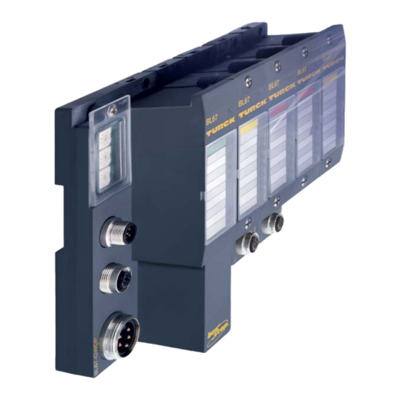
The gateway connects the fieldbus to the I/O modules. It is responsible for handling the entire process data and generates diagnostic information for the higher-level master and the software tool I/O- ASSIS-TANT (PACTware + BL67-DTM). Figure 2-2: BL67 gateway for PROFIBUS- D300529 0115 - BL67 I/O modules... -
Page 20: Electronics Modules
They are necessary when groups of modules with different potentials are planned within a BL67 station, or if the rated supply voltage of 24 V DC for the BL67 modules cannot be guaranteed. The adjoining power supply module and modules to the left are potentially isolated. -
Page 21: Base Modules
2.2.3 End plate An end plate on the right-hand side physically completes the BL67 station. It protects the module bus contacts of the last base module in a station and guarantees the protection class IP67 when tightly screwed. - Page 22 BL67-philosophy D300529 0115 - BL67 I/O modules...
-
Page 23: General Technical Data Of Bl67 Modules
General technical Data of BL67 modules General.............................. 2 Module abbreviations........................3 Technical abbreviations........................4 Station dimensions ........................... 5 General technical data ........................7 Approvals............................9 D300529 0115 - BL67 I/O modules... -
Page 24: General
This chapter describes the general information and technical data valid for the whole system. The following chapters (chapter 3 to chapter 9) contain all information about the function and the structure of BL67 I/O-, power supply and base modules as well as all module specific technical data. NOTE The gateway’s technical data, diagnostic data and parameterization options are described in... -
Page 25: Module Abbreviations
2- or 3-wire measurement type RS232 Module with integrated RS232 interface BL67-1RS232 Analog input module for connecting thermocouples BL67-2AI-TC Analog in- or output module for the measurement or the out- BL67-2AO-V put of voltage signals D300529 0115 - BL67 I/O modules... -
Page 26: Technical Abbreviations
General technical Data of BL67 modules Technical abbreviations The following abbreviations are used in the technical data and wiring diagrams: Table 3-2: Abbr. Designation Technical abbre- viations Transmission frequency Output current Maximum output current Amax Input current Short-circuit current Nominal current consumption from power supply... -
Page 27: Station Dimensions
Top view A dimensions in mm [inch] 145.0 [5.71] 135.0 [5.31] 32.0 [1.26] 32.5 [1.28] 64.0 [2.52] 32.0 [1.26] 140.0 [5.51] Figure 3-2: Side view A dimensions in mm [inch] 77.5 [3.05] 13.0 [0.51] D300529 0115 - BL67 I/O modules... - Page 28 General technical Data of BL67 modules Figure 3-3: BL67-module (electronic - and base module) A dimensions in mm [inch] 195.0 [7.68] 185.0 [7.28] 32.0 [1.26] D300529 0115 - BL67 I/O modules...
-
Page 29: General Technical Data
IEC 60529 IP67 Shock resistant according to IEC 61131 -2 Topple and fall/free fall according to IEC 61131 -2 Emitted interference High-frequency, radiated according to EN 55011, Class A Immunity to interference D300529 0115 - BL67 I/O modules... - Page 30 General technical Data of BL67 modules Static electricity according to IEC 61131 -2 Electromagnetic HF fields according to IEC 61131 -2 Fast transients (Burst) according to IEC 61131 -2 Conducted interferences according to IEC 61000-4-6 induced by HF fields 10 V Criteria A A I/O-line-length ≤...
-
Page 31: Approvals
Approvals Approvals Table 3-4: Approvals Approvals D300529 0115 - BL67 I/O modules... - Page 32 General technical Data of BL67 modules 3-10 D300529 0115 - BL67 I/O modules...
-
Page 33: Power Feeding Modules
Overview ............................2 4.1.1 Module overview....................................2 BL67-PF-24VDC, with diagnostics..................... 3 4.2.1 Technical data .......................................4 4.2.2 Diagnostic and status messages..............................4 – LED status displays ..................................4 – Diagnostic data....................................5 4.2.3 Module parameters .....................................5 4.2.4 Base modules/pin assignment ................................5 D300529 0115 - BL67 I/O modules... -
Page 34: Overview
Overview Power Feeding modules supply an galvanically isolated 24 V DC field voltage to the I/O modules. By using Power Feeding modules, it is not necessary to distribute power separately to each BL67 I/O module. Power Feeding modules distribute two separately switchable voltages to the modules, one for the... -
Page 35: Bl67-Pf-24Vdc, With Diagnostics
BL67-PF-24VDC, with diagnostics BL67-PF-24VDC, with diagnostics Figure 4-1: BL67-PF-24VDC Figure 4-2: BL67- Block diagram system bus undervoltage detection communi- module bus cation interface undervoltage detection power short circuit detection sens D300529 0115 - BL67 I/O modules... -
Page 36: Technical Data
Power supply for inputs faulty – Check the wiring to the power supply. – Check the external power supply unit. Short circuit in sensor supply – Check the sensor supply. sens Sensor supply OK D300529 0115 - BL67 I/O modules... -
Page 37: Module Parameters
Current consumption too high (> 4 A). Undervoltage V < 18 VDC Undervoltage V Sensor supply V < 18 V 4.2.3 Module parameters none 4.2.4 Base modules/pin assignment BL67-B-1RSM (7/8’’) /BL67-B-1RSM-4/BL67-B-1RSM-VO Figure 4-3: BL67-B-1RSM/ BL67-B-1RSM-4/ BL67-B-1RSM-VO D300529 0115 - BL67 I/O modules... - Page 38 ) max. 10 A sens Pin assignment BL67-PF-24VDC with BL67-B-1RSM-4 module wiring diagram Figure 4-6: Only V (pin 1 and 5) supply, do not connect pin 2 and 4! Pin assignment BL67-PF-24VDC with BL67-B-1RSM-VO module wiring diagram D300529 0115 - BL67 I/O modules...
- Page 39 BL67-4DI-N ............................33 5.6.1 Technical data ....................................34 5.6.2 Process data mapping..................................35 5.6.3 Diagnostic and status messages..............................35 – LED status displays ..................................35 5.6.4 Module parameters ..................................36 5.6.5 Base modules/pin assignment ..............................36 D300529 0115 - BL67 I/O modules...
- Page 40 Signal assignment ....................................45 BL67-16DI-P ............................ 46 5.8.1 Technical data ....................................47 5.8.2 Process data mapping ..................................47 5.8.3 Diagnostic and status messages ..............................48 – LED status displays..................................48 5.8.4 Module parameters...................................49 5.8.5 Base modules/pin assignment..............................49 5.8.6 Signal assignment .....................................50 D300529 0115 - BL67 I/O modules...
-
Page 41: Overview
Channel statuses are indicated by LEDs. Error signals from the I/O level are indicated by each mod- ule via the "D" LED. modules with channel- or connector-diagnosis: The modules BL67-xDI-PD provide whether a channel- or a connector diagnosis function. Diagnosis information are indicated via the channel LED or via the "D" LED. 5.1.1 Module overview... - Page 42 Digital input modules BL67-4DI-P Figure 5-1: BL67-4DI-P Figure 5-2: BL67- Block diagram system bus sens V sens IN 1 communi- module bus cation bus interface sens V sens sens power IN 4 sens D300529 0115 - BL67 I/O modules...
- Page 43 Power loss of the module < 250 mW Input current I Low level < 0,5 mA High level > 3.7 mA Input delay < 250 μs < 250 μs Isolation voltage (module bus/field) max. 1000 VDC D300529 0115 - BL67 I/O modules...
- Page 44 For DeviceNet, EtherNet/IP and Modbus TCP a detailed mapping table can be created with the TURCK configuration tool I/O-ASSISTANT V3 (PACTware + BL67-DTM). Table 5-3:...
-
Page 45: Base Modules/Pin Assignment
BL67-4DI-P 5.2.5 Base modules/pin assignment BL67-B-4M8 Figure 5-3: BL67-B-4M8 Figure 5-4: Pin assignment BL67-4DI-P with BL67-B-4M8 Figure 5-5: Wiring diagram BL67-4DI-P with BL67-B-4M8 BL67-B-2M12/BL67-B-2M12-P (paired) Figure 5-6: BL67-B-2M12/ BL67-B-2M12-P D300529 0115 - BL67 I/O modules... - Page 46 Figure 5-7: Pin assignment BL67-4DI-P with BL67-B-2M12/ BL67-B-2M12-P Figure 5-8: Wiring diagram BL67-4DI-P with BL67-B-2M12/ BL67-B-2M12-P BL67-B-4M12 Figure 5-9: BL67-B-4M12 Figure 5-10: Pin assignment BL67-4DI-P with BL67-B-4M12 Figure 5-11: Wiring diagram BL67-4DI-P with BL67-B-4M12 D300529 0115 - BL67 I/O modules...
- Page 47 BL67-4DI-P BL67-1M23 (-VI) Figure 5-12: BL67-1M23(-VI) Figure 5-13: Pin assignment BL67-4DI-P with BL67-B-1M23 D300529 0115 - BL67 I/O modules...
-
Page 48: Signal Assignment
Signal assignment C0P4 C0P3 C0P2 C0P1 with BL67-B-1M23 n = process data offset in input data; depending on extension of station and the corresponding fieldbus C = slot no. P = pin no. 5-10 D300529 0115 - BL67 I/O modules... -
Page 49: Bl67-4Di-P
BL67-4DI-PD BL67-4DI-PD Figure 5-14: BL67-4DI-PD Figure 5-15: BL67- Block diagram system bus communi- module bus sens cation bus interface sens power V sens A > I sens V sens D > I 5-11 D300529 0115 - BL67 I/O modules... -
Page 50: Technical Data
< 1,5 W Input current I Low level < 1,5 mA High level > 3.7 mA Input delay < 2,5 ms < 2,5 ms Isolation voltage (module bus/field) max. 2500 VDC max. 1000 VDC 5-12 D300529 0115 - BL67 I/O modules... -
Page 51: Process Data Mapping
For DeviceNet, EtherNet/IP and Modbus TCP a detailed mapping table can be created with the TURCK configuration tool I/O-ASSISTANT V3 (PACTware + BL67-DTM). Table 5-11:... -
Page 52: Diagnostic And Status Messages
Short-circuit or overload at sensor supply A, B, C or D (see Table 5-19) Wire break ch x Groupwise wire break detection: Group A (channel 0 and 2) Group B (channel 1 and 3) 5-14 D300529 0115 - BL67 I/O modules... -
Page 53: Module Parameters
BL67-4DI-PD 5.3.4 Module parameters NOTE Due to a product actualization, the parameter texts of the TURCK-I/O-product have been revised. The actual configuration files (GSD-, GSDML-, EDS-files) with the new parameters can be found under www.turck.com. If you use older configuration files with old parameter texts (issue date before April 2014),... - Page 54 0 =no Input signal not inverted. 1 = yes Input signal inverted, conversion of the effective sig- nal direction for sensors. Activate wire break monitor- 0 =no 1 = yes Groupwise wire break monitoring 5-16 D300529 0115 - BL67 I/O modules...
-
Page 55: Base Modules/Pin Assignment
BL67-4DI-PD 5.3.5 Base modules/pin assignment BL67-B-4M8 Figure 5-16: BL67-B-4M8 Figure 5-17: Pin assignment BL67-4DI-PD with BL67-B-4M8 Figure 5-18: Wiring diagram BL67-4DI-PD with BL67-B-4M8 BL67-B-2M12/BL67-B-2M12-P Figure 5-19: BL67-B-2M12/ BL67-B-2M12-P 5-17 D300529 0115 - BL67 I/O modules... - Page 56 If the wire break detection has been activated, a jumper between pin 1 (24 VDC) and pin 2 (diagnostics Wiring diagram for input) must be implemented on the sensor side for monitoring of wire-breaks. wire break detec- tion only with base module BL67-B-2M12) BL67-B-4M12 Figure 5-23: BL67-B-4M12 5-18 D300529 0115 - BL67 I/O modules...
-
Page 57: Signal Assignment
C = slot no. P = pin no. 5.3.7 sensor supply Table 5-19: sens sensor supply BL67-B-2M12 C0P1 C1P1 BL67-B-2M12-P C0P1 C1P1 BL67-B-4M12 C0P1 C1P1 C2P1 C3P1 BL67-B-4M8 C0P1 C1P1 C2P1 C3P1 5-19 D300529 0115 - BL67 I/O modules... -
Page 58: Bl67-8Di-P
Digital input modules BL67-8DI-P Figure 5-26: BL67-8DI-P Figure 5-27: BL67- Block diagram system bus sens V sens IN 1 communi- module bus cation bus interface sens V sens sens power IN 8 sens 5-20 D300529 0115 - BL67 I/O modules... -
Page 59: Technical Data
For DeviceNet, EtherNet/IP and Modbus TCP a detailed mapping table can be created with the TURCK configuration tool I/O-ASSISTANT V3 (PACTware + BL67-DTM). Table 5-21:... -
Page 60: Module Parameters
This concerns modules located between this module and the gateway. No error messages – 0 to 7 Green Status of channel x = "1" – Status of channel x = "0" 5.4.4 Module parameters none 5-22 D300529 0115 - BL67 I/O modules... -
Page 61: Base Modules/Pin Assignment
BL67-8DI-P 5.4.5 Base modules/pin assignment BL67-B-8M8 Figure 5-28: BL67-B-8M8 Figure 5-29: Pin assignment BL67-8DI-P with BL67-B-8M8 Figure 5-30: Wiring diagram BL67-8DI-P with BL67-B-8M8 5-23 D300529 0115 - BL67 I/O modules... - Page 62 Digital input modules BL67-B-4M12/BL67-B-4M12-P (paired) Figure 5-31: BL67-B-4M12/ BL67-B-4M12-P Figure 5-32: Pin assignment BL67-8DI-P with BL67-B-4M12/ BL67-B-4M12-P Figure 5-33: Wiring diagram BL67-8DI-P with BL67-B-4M12/ BL67-B-4M12-P 5-24 D300529 0115 - BL67 I/O modules...
-
Page 63: Signal Assignment
C0P6 C0P5 C0P4 C0P3 C0P2 C0P1 with BL67-B-1M23 n = process data offset in input data; depending on extension of station and the corresponding fieldbus C = slot no. P = pin no. 5-25 D300529 0115 - BL67 I/O modules... -
Page 64: Bl67-8Di-Pd
Digital input modules BL67-8DI-PD Figure 5-36: BL67-8DI-PD Figure 5-37: BL67- Block diagram system bus communi- module bus sens cation bus interface sens power V sens A > I sens V sens D > I 5-26 D300529 0115 - BL67 I/O modules... -
Page 65: Technical Data
For DeviceNet, EtherNet/IP and Modbus TCP a detailed mapping table can be created with the TURCK configuration tool I/O-ASSISTANT V3 (PACTware + BL67-DTM). Table 5-28:... -
Page 66: Diagnostic And Status Messages
A, B, C or D (see Table 5-35) Wire break Groupwise wire break detection: Group A (channel 0 and 4) Group B (channel 1 and 5) Group C (channel 2 and 6) Group D (channel 3 and 7) 5-28 D300529 0115 - BL67 I/O modules... -
Page 67: Module Parameters
BL67-8DI-PD 5.5.4 Module parameters NOTE Due to a product actualization, the parameter texts of the TURCK-I/O-product have been revised. The actual configuration files (GSD-, GSDML-, EDS-files) with the new parameters can be found under www.turck.com. If you use older configuration files with old parameter texts (issue date before April 2014),... -
Page 68: Base Modules/Pin Assignment
Activate wire break monitor- 0 =no 1 = yes Groupwise wire break monitoring 5.5.5 Base modules/pin assignment BL67-B-8M8 Figure 5-38: BL67-B-8M8 Figure 5-39: Pin assignment BL67-8DI-PD with BL67-B-8M8 Figure 5-40: Wiring diagram BL67-8DI-PD with BL67-B-8M8 5-30 D300529 0115 - BL67 I/O modules... - Page 69 If the wire break detection has been activated, a jumper between pin 1 (24 VDC) and pin 2 (diagnostics Wiring diagram for input) must be implemented on the sensor side for monitoring of wire-breaks. wire break detec- tion only with base module BL67-B-4M12 5-31 D300529 0115 - BL67 I/O modules...
-
Page 70: Signal Assignment
C = slot no. P = pin no. 5.5.7 Sensor supply Table 5-35: sens Sensor supply BL67-B-4M12 C0P1 C1P1 C2P1 C3P1 BL67-B-4M12-P C0P1 C1P1 C2P1 C3P1 BL67-B-8M8 C0P1/ C2P1/ C4P1/ C6P1/ C1P1 C3P1 C5P1 C7P1 5-32 D300529 0115 - BL67 I/O modules... -
Page 71: Bl67-4Di-N
BL67-4DI-N BL67-4DI-N Figure 5-45: BL67-4DI-N Figure 5-46: BL67- Block diagram system bus sens V sens IN 1 communi- module bus cation bus interface sens sens V sens power IN 4 sens 5-33 D300529 0115 - BL67 I/O modules... -
Page 72: Technical Data
< 1,3 W Input current I Low level < 2,5 mA High level > 3 mA Input delay < 250 μs < 250 μs Isolation voltage (module bus/field) max. 2500 VDC max. 1000 VDC 5-34 D300529 0115 - BL67 I/O modules... -
Page 73: Process Data Mapping
For DeviceNet, EtherNet/IP and Modbus TCP a detailed mapping table can be created with the TURCK configuration tool I/O-ASSISTANT V3 (PACTware + BL67-DTM). Table 5-37:... -
Page 74: Module Parameters
Digital input modules 5.6.4 Module parameters none 5.6.5 Base modules/pin assignment BL67-B-4M8 Figure 5-47: BL67-B-4M8 Figure 5-48: Pin assignment BL67-4DI-N with BL67-B-4M8 Figure 5-49: Wiring diagram BL67-4DI-N with BL67-B-4M8 5-36 D300529 0115 - BL67 I/O modules... - Page 75 BL67-4DI-N BL67-B-2M12/BL67-B-2M12-P (paired) Figure 5-50: BL67-B-2M12/ BL67-B-2M12-P Figure 5-51: Pin assignment BL67-4DI-N with BL67-B-2M12/ BL67-B-2M12-P Figure 5-52: Wiring diagram BL67-4DI-N with BL67-B-2M12/ BL67-B-2M12-P 5-37 D300529 0115 - BL67 I/O modules...
- Page 76 Digital input modules BL67-B-4M12 Figure 5-53: BL67-B-4M12 Figure 5-54: Pin assignment BL67-4DI-N with BL67-B-4M12 Figure 5-55: Wiring diagram BL67-4DI-N with BL67-B-4M12 BL67-1M23 Figure 5-56: BL67-B-1M23 5-38 D300529 0115 - BL67 I/O modules...
-
Page 77: Signal Assignment
Bit 0 Signal assignment C0P4 C0P3 C0P2 C0P1 with BL67-B-1M23 n = offset of input data; depending on extension of station and the corresponding fieldbus. C = slot no. P = pin no. 5-39 D300529 0115 - BL67 I/O modules... -
Page 78: Bl67-8Di-N
Digital input modules BL67-8DI-N Figure 5-58: BL67-8DI-N Figure 5-59: BL67- Block diagram system bus sens V sens IN 1 communi- module bus cation bus interface sens V sens sens power IN 8 sens 5-40 D300529 0115 - BL67 I/O modules... -
Page 79: Technical Data
< 1,3 W Input current I Low level < 1,2 mA High level > 1.5 mA Input delay < 250 μs < 250 μs Isolation voltage (module bus/field) max. 2500 VDC max. 1000 VDC 5-41 D300529 0115 - BL67 I/O modules... -
Page 80: Process Data Mapping
For DeviceNet, EtherNet/IP and Modbus TCP a detailed mapping table can be created with the TURCK configuration tool I/O-ASSISTANT V3 (PACTware + BL67-DTM). Table 5-45:... -
Page 81: Module Parameters
BL67-8DI-N 5.7.4 Module parameters none 5.7.5 Base modules/pin assignment BL67-B-8M8 Figure 5-60: BL67-B-8M8 Figure 5-61: Pin assignment BL67-8DI-N with BL67-B-8M8 Figure 5-62: Wiring diagram BL67-8DI-N with BL67-B-8M8 5-43 D300529 0115 - BL67 I/O modules... - Page 82 Digital input modules BL67-B-4M12/BL67-B-4M12-P (paired) Figure 5-63: BL67-B-4M12/ BL67-B-4M12-P Figure 5-64: Pin assignment BL67-8DI-N with BL67-B-4M12/ BL67-B-4M12-P Figure 5-65: Wiring diagram BL67-8DI-N with BL67-B-4M12/ BL67-B-4M12-P 5-44 D300529 0115 - BL67 I/O modules...
-
Page 83: Signal Assignment
C0P8 C0P7 C0P6 C0P5 C0P4 C0P3 C0P2 C0P1 with BL67-1M23(-VI) n = offset of input data; depending on extension of station and the corresponding fieldbus. C = slot no. P = pin no. 5-45 D300529 0115 - BL67 I/O modules... -
Page 84: Bl67-16Di-P
Digital input modules BL67-16DI-P Figure 5-68: BL67-16DI-P Figure 5-69: BL67- Block diagram system bus sens V sens IN 1 communi- module bus cation bus interface sens sens V sens power IN 16 sens 5-46 D300529 0115 - BL67 I/O modules... -
Page 85: Technical Data
For DeviceNet, EtherNet/IP and Modbus TCP a detailed mapping table can be created with the TURCK configuration tool I/O-ASSISTANT V3 (PACTware + BL67-DTM). Table 5-52:... -
Page 86: Diagnostic And Status Messages
No error messages – 0 to 7 Green status of channel 0 to 7 = 1 – orange status of channel 8 to 15 = 1 status of channel x = "0" 5-48 D300529 0115 - BL67 I/O modules... -
Page 87: Module Parameters
5.8.5 Base modules/pin assignment BL67-B-8M8 -4-P Figure 5-70: BL67-B-8M8-4-P Figure 5-71: Pin assignment 1 = V SENS BL67-16DI-P with 2 = Signal A BL67-B-8M8-4-P 3 = GND 4 = Signal B 5-49 D300529 0115 - BL67 I/O modules... -
Page 88: Signal Assignment
C0P18 C0P1 C0P10 C0P11 C0P13 C0P2 C0P9 C0P17 n = process data offset in input data; depending on extension of station and the corresponding fieldbus C = slot no. P = pin no. 5-50 D300529 0115 - BL67 I/O modules... - Page 89 6.2.5 Base modules/pin assignment ..............................12 6.2.6 Measurement value representation............................14 – 16-bit-representation .................................. 14 – 12-bit-representation (left-justified) ............................14 BL67-2AI-V, -10/0 … +10 VDC ......................15 6.3.1 Technical data ....................................16 6.3.2 Process data mapping..................................17 6.3.3 Diagnostic and status messages..............................18 –...
- Page 90 – Basic errors and repeat accuracies ............................69 6.7.2 Process data mapping ..................................70 6.7.3 Diagnostic and status messages ..............................70 – Diagnostic data ....................................70 6.7.4 Module parameters ..................................72 6.7.5 Base modules/pin assignment..............................74 6.7.6 Measurement value representation ............................74 – Temperature measurement...............................74 D300529 0115 - BL67 I/O modules...
-
Page 91: Overview
(Types: B, E, J, K, N, R, S, T) LED displays Error signals from the I/O level are indicated by each module via the "D" LED. The corresponding diag- nostic information is transmitted to the gateway via diagnostic bits. D300529 0115 - BL67 I/O modules... -
Page 92: Analog Data Representation
A detailed description of the measurement value representation for the analog input mod- ules in 16 or 12 bit can be found in the Appendix of this manual, Analog value representation (analog input modules) (page 15-8). D300529 0115 - BL67 I/O modules... - Page 93 The figure shows a 5-digit binary code in the outer circuit. The inner circuit shows the respective dual number, if the binary code is interpreted as binary number (positive numerical values) and as two’s complement. Figure 6-3: Binary code as dual number ans two's comple- ment D300529 0115 - BL67 I/O modules...
-
Page 94: Module Overview
Analog input modules 6.1.2 Module overview Table 6-1: Module No. of channels Module overview BL67-2AI-I BL67-2AI-V BL67-2AI-PT BL67-2AI-TC BL67-4AI-V/I BL67-4AI-TC D300529 0115 - BL67 I/O modules... -
Page 95: Bl67-2Ai-I, 0/4
BL67-2AI-I, 0/4 … 20mA BL67-2AI-I, 0/4 … 20mA Figure 6-4: BL67-2AI-I Figure 6-5: BL67- Block diagram system bus sens signal conditioning communi- module bus multi- cation interface plexer converter sens power sens D300529 0115 - BL67 I/O modules... -
Page 96: Technical Data
– 12 bit left-justified two's complement coded (even negative values possible), binary number without coding (only positive values possible) ≤ 250 mA; short-circuit protected in gateway or (sensor supply from V SENS sens Power Feeding module D300529 0115 - BL67 I/O modules... -
Page 97: Process Data Mapping
For DeviceNet, EtherNet/IP and Modbus TCP a detailed mapping table can be created with the TURCK configuration tool I/O-ASSISTANT V3 (PACTware + BL67-DTM). Table 6-3:... -
Page 98: Diagnostic And Status Messages
Displays a wire break in the signal line for the operating mode 4 to 20 mA. NOTE In the 12-bit-representation (left-justified) the diagnostic data are transmitted with the lower nibble of the process data for the respective channel. 6-10 D300529 0115 - BL67 I/O modules... -
Page 99: Module Parameters
BL67-2AI-I, 0/4 … 20mA 6.2.4 Module parameters NOTE Due to a product actualization, the parameter texts of the TURCK-I/O-product have been revised. The actual configuration files (GSD-, GSDML-, EDS-files) with the new parameters can be found under www.turck.com. If you use older configuration files with old parameter texts (issue date before April 2014),... -
Page 100: Base Modules/Pin Assignment
Analog input modules 6.2.5 Base modules/pin assignment BL67-B-2M12 Figure 6-6: BL67-B-2M12 Figure 6-7: Pin assign- ment BL67-2AI-I 6-12 D300529 0115 - BL67 I/O modules... - Page 101 2-wire sensor with sensor supply via base module: Wiring diagrams BL67-2AI-I 3-wire sensor with sensor supply via base module 4-wire sensor with sensor supply via base module: 4-wire sensor with external sensor supply: 6-13 D300529 0115 - BL67 I/O modules...
-
Page 102: Measurement Value Representation
(decimal: 0 to 4095) NOTE A detailed description of the measurement value representation for the analog input mod- ules in 16 or 12 bit can be found in the Appendix of this manual, page 15-8. 6-14 D300529 0115 - BL67 I/O modules... -
Page 103: Bl67-2Ai-V, -10/0
BL67-2AI-V, -10/0 … +10 VDC BL67-2AI-V, -10/0 … +10 VDC Figure 6-9: BL67-2AI-V Figure 6-10: BL67- Block diagram system bus sens signal conditioning communi- module bus multi- cation interface plexer converter sens power sens 6-15 D300529 0115 - BL67 I/O modules... -
Page 104: Technical Data
(even negative values possi- ble) binary number without coding (only posi- tive values possible) ≤ 250 mA; short-circuit protected in gateway or (sensor supply from V SENS sens Power Feeding module 6-16 D300529 0115 - BL67 I/O modules... -
Page 105: Process Data Mapping
For DeviceNet, EtherNet/IP and Modbus TCP a detailed mapping table can be created with the TURCK configuration tool I/O-ASSISTANT V3 (PACTware + BL67-DTM). Table 6-8:... -
Page 106: Diagnostic And Status Messages
– U (U < -0,1 V) for 0 bis +10 VDC NOTE In the 12-bit-representation (left-justified) the diagnostic data are transmitted with the lower nibble of the process data for the respective channel. 6-18 D300529 0115 - BL67 I/O modules... -
Page 107: Module Parameters
BL67-2AI-V, -10/0 … +10 VDC 6.3.4 Module parameters NOTE Due to a product actualization, the parameter texts of the TURCK-I/O-product have been revised. The actual configuration files (GSD-, GSDML-, EDS-files) with the new parameters can be found under www.turck.com. If you use older configuration files with old parameter texts (issue date before April 2014),... -
Page 108: Base Modules/Pin Assignment
Analog input modules 6.3.5 Base modules/pin assignment BL67-B-2M12 Figure 6-11: BL67-B-2M12 Table 6-12: Pin assignment BL67-2AI-V 6-20 D300529 0115 - BL67 I/O modules... - Page 109 2-wire sensor with sensor supply via base module: Wiring diagrams BL67-2AI-V 3-wire sensor with sensor supply via base module 4-wire sensor with sensor supply via base module: 4-wire sensor with external sensor supply: 6-21 D300529 0115 - BL67 I/O modules...
-
Page 110: Measurement Value Representation
(decimal: -2048 to -1) NOTE A detailed description of the measurement value representation for the analog input mod- ules in 16 or 12 bit can be found in the Appendix of this manual, page 15-8. 6-22 D300529 0115 - BL67 I/O modules... -
Page 111: Bl67-2Ai-Pt, Pt-/Ni-Sensors
BL67-2AI-PT, Pt-/Ni-sensors BL67-2AI-PT, Pt-/Ni-sensors Figure 6-13: BL67-2AI-PT Figure 6-14: BL67- Block diagram system bus signal conditioning communi- module bus multi- é cation interface plexer converter é power sens 6-23 D300529 0115 - BL67 I/O modules... -
Page 112: Technical Data
± 0,2 % from end value Repeat accuracy 0,05 % ≤ 300 ppm/°C from end value Temperature coefficient ≤ 130 ms per channel (cycle time) CYCL Connectable sensors Platinum sensors Pt100, Pt200, Pt500, Pt1000 Nickel sensors Ni100, Ni1000 6-24 D300529 0115 - BL67 I/O modules... -
Page 113: Process Data Mapping
For DeviceNet, EtherNet/IP and Modbus TCP a detailed mapping table can be created with the TURCK configuration tool I/O-ASSISTANT V3 (PACTware + BL67-DTM). Table 6-14:... -
Page 114: Diagnostic Data
NOTE In 3-wire measurement with PT100- sensor and at temperatures of below -177 °C, the module can not distinguish between overcurrent and wire break. In this case, the diagnostic "overcur- rent" is generated. 6-26 D300529 0115 - BL67 I/O modules... -
Page 115: Module Parameters
BL67-2AI-PT, Pt-/Ni-sensors 6.4.5 Module parameters NOTE Due to a product actualization, the parameter texts of the TURCK-I/O-product have been revised. The actual configuration files (GSD-, GSDML-, EDS-files) with the new parameters can be found under www.turck.com. If you use older configuration files with old parameter texts (issue date before April 2014),... - Page 116 1100 = resistance, 0 … 100 Ω 1101 = resistance, 0 … 200 Ω 1110 = resistance, 0 … 400 Ω 1111 = resistance, 0 … 1000 Ω Measurement mode 0 = 2 wire 1 = 3 wire 6-28 D300529 0115 - BL67 I/O modules...
-
Page 117: Base Modules/Pin Assignment
BL67-2AI-PT, Pt-/Ni-sensors 6.4.6 Base modules/pin assignment BL67-B-2M12 Figure 6-15: BL67-B-2M12 Table 6-18: Pin assignment BL67-2AI-PT Table 6-19: 2-wire-connection technology: Wiring diagrams BL67-2AI-PT 3-wire-connection technology: 6-29 D300529 0115 - BL67 I/O modules... -
Page 118: Measurement Value Representation
The value range: 0 to 100 Ω; 0 to 200 Ω; 0 to 400 Ω; 0 to 1000 Ω is displayed as follows: 0000 to 7FFF (decimal: 0 to 32767) 6-30 D300529 0115 - BL67 I/O modules... - Page 119 -200 °C to -0,1 °C is displayed as follows: 830(0) bis FFF(0) (decimal: -2000 to -1) The value range: 0 °C to 150 °C is displayed as follows: 000(0) bis 5DC(0) (decimal: 0 to 1500) 6-31 D300529 0115 - BL67 I/O modules...
- Page 120 (decimal: 0 to 4095). NOTE A detailed description of the measurement value representation for the analog input modules in 16 or 12 bit can be found in the Appendix of this manual, page 15-8. 6-32 D300529 0115 - BL67 I/O modules...
-
Page 121: Bl67-2Ai-Tc, Thermo Couples
BL67-2AI-TC, thermo couples BL67-2AI-TC, thermo couples Figure 6-16: BL67-2AI-TC Figure 6-17: BL67- Block diagram Systembus Signalauf- bereitung Kommuni- Modulbus- Multi- kations- é Interface plexer Wandler é Power- sens Kaltstellenkompensations-Messwiderstand (Pt1000) im Stecker 6-33 D300529 0115 - BL67 I/O modules... -
Page 122: Technical Data
< 4 μV ± 100 mV < 20 μV ± 500 mV < 50 μV ± 1 V Measurement value representation 16 bit signed integer/ 12 bit full range, left-justified at 23 °C Table 6-21: 6-34 D300529 0115 - BL67 I/O modules... - Page 123 Type R 0.05 ± 0,12 Type S 0.05 ± 0,13 Type T – 0.075 Voltage measurement 0.05 – NOTE Wider deviations of the cold junction compensation are to be expected for lower tempera- tures. 6-35 D300529 0115 - BL67 I/O modules...
-
Page 124: Process Data Mapping
For DeviceNet, EtherNet/IP and Modbus TCP a detailed mapping table can be created with the TURCK configuration tool I/O-ASSISTANT V3 (PACTware + BL67-DTM). Process data... -
Page 125: Module Parameters
23 °C is automatically presumed. 6.5.4 Module parameters NOTE Due to a product actualization, the parameter texts of the TURCK-I/O-product have been revised. The actual configuration files (GSD-, GSDML-, EDS-files) with the new parameters can be found under www.turck.com. - Page 126 0101 = Type R, -50 … 1760 °C 0110 = Type S, -50 … 1540 °C 0111 = Type T, -270 … 400 °C 1000 = +/-50 mV 1001 = +/-100 mV 1010 = +/-500 mV 1011 = +/-1000 mV 6-38 D300529 0115 - BL67 I/O modules...
-
Page 127: Base Modules/Pin Assignment
BL67-B-2M12 Table 6-27: Pin assignment S = PT1000 sensor for cold junction compensation BL67-2AI-TC TC = thermo couple Table 6-28: Suitable connector with a Pt1000 for the Wiring diagram cold-junction compensation: BL67-2AI-TC BL67-WAS5-THERMO 6-39 D300529 0115 - BL67 I/O modules... -
Page 128: Measurement Value Representation
The value range: 0 mV to 50 mV; 0 mV to 100 mV; 0 mV to 500 mV; 0 mV to 1000 mV; is displayed as follows: 0000 to 7FFF (decimal: 0 to 32767) 6-40 D300529 0115 - BL67 I/O modules... - Page 129 (decimal: 0 to 2047) NOTE A detailed description of the measurement value representation for the analog input mod- ules in 16 or 12 bit can be found in the Appendix of this manual, page 15-8. 6-41 D300529 0115 - BL67 I/O modules...
-
Page 130: Bl67-4Ai-V/I, Voltage-/Current Measurement
Analog input modules BL67-4AI-V/I, voltage-/current measurement Figure 6-19: BL67-4AI-V/I Figure 6-20: BL67- Block diagram system bus sens signal conditioning communi- module bus multi- cation interface plexer converter sens power sens 6-42 D300529 0115 - BL67 I/O modules... -
Page 131: Technical Data
(module bus/field) min. 500 V (field/functional earth) min. 50 V channel/channel none channel/field supply none channel/system supply 500 V accuracy for the input signal Basic error at 23 °C/73.4 °F ± 0,3 % 6-43 D300529 0115 - BL67 I/O modules... -
Page 132: Process Data Mapping
For DeviceNet, EtherNet/IP and Modbus TCP a detailed mapping table can be created with the TURCK configuration tool I/O-ASSISTANT V3 (PACTware + BL67-DTM). Table 6-30:... -
Page 133: Diagnostic And Status Messages
No error messages or diagnos- – tics 0 to 4 Green Channel x active Green Underflow flashing, 0.5 Hz Green Overflow flashing, 4 Hz Channel x inactive 6-45 D300529 0115 - BL67 I/O modules... - Page 134 After this, a periodical switching to current measurement is done. If the current falls again to the permissible range, the module switches permanently back to current measurement. During this procedure, the transmitted value is always the measurement range end value. Please observe the module’s maximum input voltage! 6-46 D300529 0115 - BL67 I/O modules...
-
Page 135: Module Parameters
BL67-4AI-V/I, voltage-/current measurement 6.6.4 Module parameters NOTE Due to a product actualization, the parameter texts of the TURCK-I/O-product have been revised. The actual configuration files (GSD-, GSDML-, EDS-files) with the new parameters can be found under www.turck.com. If you use older configuration files with old parameter texts (issue date before April 2014),... - Page 136 1 = current Data representation 00 = standard 01 = NE 43 10 = extended range NOTE Concerning the "number representation", please observe the tables for measurement value representation on the following pages. 6-48 D300529 0115 - BL67 I/O modules...
-
Page 137: Measurement Value Representation
… … 0.000305 V 0001 ≤ 0.000000 V 0000 ≥ -0,0500 V at ↑ DIA Measured value 0000 out of range at ↓ DIA < -0,1000 V Measured value 0000 out of range 6-49 D300529 0115 - BL67 I/O modules... - Page 138 ↓ DIA < 3.6000 mA Measured value 0000 out of range ≥ 3,0000 mA at ↑ DIA Wire break 0000 at ↓ DIA < 2.9000 mA Wire break 0000 6-50 D300529 0115 - BL67 I/O modules...
- Page 139 0.00244 V 1 × 16 001× ≤ 0.0000 V 000× ≥ -0,0500 V at ↑ DIA Measured value 000× out of range at ↓ DIA < -0,1000 V Measured value 000× out of range 6-51 D300529 0115 - BL67 I/O modules...
- Page 140 ↓ DIA < 3,6000 mA Measured value out 000× of range ≥ 3,0000 mA at ↑ DIA Wire break 000× at ↓ DIA < 2,9000 mA Wire break 000× 6-52 D300529 0115 - BL67 I/O modules...
- Page 141 ↑ DIA under- Measured value -32080 82B0 steering out of range -11.758897 V -32511 8100 at ↓ DIA -11.759259 V Measured value -32512 80FF out of range underflow ≤ -11.851851 V -32768 8000 6-53 D300529 0115 - BL67 I/O modules...
- Page 142 5.0000 V 13824 3600 … … … 0.000361 V 0001 0.000000 V 0000 < 0,000000 V 0000 ≥ -0,050 V at ↑ DIA 0000 Overflow/underflow underflow at ↓ DIA < -0,100 V 0000 Overflow/underflow 6-54 D300529 0115 - BL67 I/O modules...
- Page 143 ↑ DIA under- Measured value -4672 EDC0 steering out of range 1.185185 -4864 ED00 ≤ 1.184606 mA at ↓ DIA Measured value -4865 ECFF underflow out of range ≤ 0.0000 mA -6912 E500 6-55 D300529 0115 - BL67 I/O modules...
- Page 144 82B0 steering out of range -11.7592 V -2032 × 16 8100 at ↓ DIA -11.7650 V Measured value -2033 × 16 80F0 out of range underflow ≤ -11.8518 V -2048 × 16 8000 6-56 D300529 0115 - BL67 I/O modules...
- Page 145 864 × 16 3600 … … … 0.000578 V 1 × 16 0010 0.00000 V 0000 ≥ -0.050 V at ↑ DIA 0000 Overflow/underflow underflow at ↓ DIA < -0,100 V 0000 Overflow/underflow 6-57 D300529 0115 - BL67 I/O modules...
- Page 146 1.1851 mA -304 × 16 ED00 ≤ 1.1759 mA at ↓ DIA Measured value -305 × 16 ECF0 out of range underflow ≤ 0.000 mA -432 × 16 E500 6-58 D300529 0115 - BL67 I/O modules...
- Page 147 -10250 D7F6 under- out of range steering at ↓ DIA -10.500 V Measured value -10500 D6FC out of range -10.501 V -10501 D6FB -10.999 V underflow -10999 D509 ≤ -11.000 V -11000 D508 6-59 D300529 0115 - BL67 I/O modules...
- Page 148 ↓ DIA Measured value 20500 5014 steering out of range 20.001 mA 20001 4E21 20.000 mA 20000 4E20 … … … 10.000 mA 10000 2712 … … … 0.001 mA 0001 0.0000 mA 0000 6-60 D300529 0115 - BL67 I/O modules...
- Page 149 0E10 out of range 3.599 mA 3599 0E0F ≥ 2,001 mA at ↑ DIA Wire break 2001 07D1 underflow ≤ 2.000 mA at ↓ DIA Wire break 2000 07D0 0.000 mA 0000 0000 6-61 D300529 0115 - BL67 I/O modules...
- Page 150 Measured value -10256 D7F× steering out of range -10.496 V -10496 D70× at ↓ DIA -10.512 V Measured value -10512 D6F× out of range underflow -10.992 V -10992 D51× ≤ -11.008 V -11008 D50× 6-62 D300529 0115 - BL67 I/O modules...
- Page 151 ↓ DIA Measured value 20496 501× steering out of range 20.016 mA 20016 4E3× 20,000 mA 20000 4E2× … … … 10.000 mA 10000 271× … … … 0.016 mA 001× 0.0000 mA 000× 6-63 D300529 0115 - BL67 I/O modules...
- Page 152 0E1× out of range 3.584 mA 3584 0E0× ≥ 2,001 mA at ↑ DIA Wire break 2001 07D× underflow < 2,000 mA at ↓ DIA Wire break 2000 07D× 0.000 mA 0000 000× 6-64 D300529 0115 - BL67 I/O modules...
-
Page 153: Base Modules/Pin Assignment
BL67-4AI-V/I, voltage-/current measurement 6.6.6 Base modules/pin assignment BL67-B-4M12 Figure 6-21: BL67-B-4M12 Table 6-34: Pin assignment BL67-4AI-V/I with BL67-B-4M12 6-65 D300529 0115 - BL67 I/O modules... - Page 154 2-wire sensor with sensor supply via base module: Wiring diagrams BL67-4AI-V/I 3-wire sensor with sensor supply via base module 4-wire sensor with sensor supply via base module: 4-wire sensor with external sensor supply: 6-66 D300529 0115 - BL67 I/O modules...
-
Page 155: Bl67-4Ai-Tc, Thermo Element
Figure 6-24: BL67- Block diagram system bus signal conditioning communi- module bus multi- cation interface Channel 1 plexer converter Channel 4 power sens cold junction compensation r esistance (Pt1000) in male connector 6-67 D300529 0115 - BL67 I/O modules... -
Page 156: Technical Data
12 bit full range, left-justified Basic error (nominal range at 23 °C) see table page 6-69 Limit frequency analog 70 Hz Repeat accuracy 0,5 % from end value ≤ 150 ppm/°C from end value Temperature coefficient 6-68 D300529 0115 - BL67 I/O modules... - Page 157 75 … 1760 °C 0.05 Type T -200 … 400 °C 0.05 Voltage measurement all measurement ranges 0.05 For temperatures outside the defined measurement range, higher deviations for basic error and repeat accuracy are possible. 6-69 D300529 0115 - BL67 I/O modules...
-
Page 158: Process Data Mapping
For DeviceNet, EtherNet/IP and Modbus TCP a detailed mapping table can be created with the TURCK configuration tool I/O-ASSISTANT V3 (PACTware + BL67-DTM). Table 6-37:... - Page 159 – If the sensors are not insulated, use channels of different sensor groups (e.g. channel 1 and chan- nel 3). Hardware failure Shows common errors of the module hardware. The return analog value in case of an error is "0". 6-71 D300529 0115 - BL67 I/O modules...
-
Page 160: Module Parameters
Analog input modules 6.7.4 Module parameters NOTE Due to a product actualization, the parameter texts of the TURCK-I/O-product have been revised. The actual configuration files (GSD-, GSDML-, EDS-files) with the new parameters can be found under www.turck.com. If you use older configuration files with old parameter texts (issue date before April 2014),... - Page 161 1011 = +/-1000 mV 1100 = Type K, -454 … 2498 °F 1101 = Type K, -454 … 2498 °F 1110 = Type C 0 … 2315 °C 1111 = Type G 0 … 2315 °C 6-73 D300529 0115 - BL67 I/O modules...
-
Page 162: Base Modules/Pin Assignment
Example (°C): 10,1 °C → 10 → (0x000A <<4) → 0x00A0 Fahrenheit: The measured temperature is divided by 2 shifted 4 bit to the left. Example (°F): 10,1 °C → 5 → (0x0005 << 4) → 0x0050 6-74 D300529 0115 - BL67 I/O modules... - Page 163 999.939 32766 7FFE 32752 7FF0 49.998 99.997 499.985 999.969 32767 7FFF 32752 7FF0 NOTE In 12 bit representation, the module‘s diagnostic data are mapped into bit 0 - 3 of the input data. 6-75 D300529 0115 - BL67 I/O modules...
- Page 164 Analog input modules 6-76 D300529 0115 - BL67 I/O modules...
-
Page 165: Digital Output Modules
BL67-16DO-0.1A-P .......................... 36 7.6.1 Technical data ....................................37 7.6.2 Process data mapping..................................38 7.6.3 Diagnostic and status messages..............................39 – LED status displays ..................................39 – Diagnostic data....................................39 – Diagnostics via software................................39 D300529 0115 - BL67 I/O modules... - Page 166 BL67-8DO-0.5A-N..........................52 7.8.1 Technical data.....................................53 7.8.2 Process data mapping ..................................54 7.8.3 Diagnostic and status messages ..............................55 – LED status displays..................................55 – Diagnostic data ....................................55 7.8.4 Module parameters...................................55 7.8.5 Base modules/pin assignment..............................56 7.8.6 Signal assignment .....................................58 D300529 0115 - BL67 I/O modules...
-
Page 167: Overview
"D" LED. The corresponding diagnostic information is transmitted to the gateway via diagnostic bits. ATTENTION! High voltage when switching-off inductive loads Destruction of the electronic in the module Provide an external suppressor. D300529 0115 - BL67 I/O modules... - Page 168 BL67-4DO-4A-P BL67-8DO-0.5A-P 0.5 A BL67-16DO-0.1A-P 0.1 A BL67-4DO-2A-N BL67-8DO-0.5A-N 0.5 A Module Isolation Positive switching BL67-4DO-0.5A-P BL67-4DO-2A-P BL67-4DO-4A-P BL67-8DO-0.5A-P BL67-16DO-0.1A-P BL67-4DO-2A-N BL67-8DO-0.5A-N D300529 0115 - BL67 I/O modules...
-
Page 169: Bl67-4Do-0.5A-P
Figure 7-1: BL67-4DO-0.5A Figure 7-2: BL67- Block diagram system bus V sens OUT 1 0.5 A P communi- module bus cation bus interface sens V sens OUT 4 power 0.5 A P sens sens D300529 0115 - BL67 I/O modules... -
Page 170: Technical Data
190 mΩ Resistive, inductive and lamp loads can be connected 48 Ω Load impedance, resistive R Lamp load R Switching frequency resistive load 200 Hz inductive load 2 Hz lamp load 20 Hz Isolation voltage D300529 0115 - BL67 I/O modules... -
Page 171: Process Data Mapping
For DeviceNet, EtherNet/IP and Modbus TCP a detailed mapping table can be created with the TURCK configuration tool I/O-ASSISTANT V3 (PACTware + BL67-DTM). Table 7-3:... -
Page 172: Diagnostic And Status Messages
Diagnostics Table 7-5: Diagnostics Overcurrent Overcurrent or short-circuit at the output. The channel is switched off automatically. For the for switching-off characteristics of the outputs see Technical data Table 7-2. 7.2.4 Module parameters none D300529 0115 - BL67 I/O modules... -
Page 173: Base Modules/Pin Assignment
BL67-4DO-0.5A-P 7.2.5 Base modules/pin assignment BL67-B-4M8 Figure 7-3: BL67-B-4M8 Figure 7-4: Pin assignment BL67-4DO-0.5A-P with BL67-B-4M8 Figure 7-5: Wiring diagram BL67-4DO-0.5A-P with BL67-B-4M8 BL67-B-2M12/BL67-B-2M12-P (paired) Figure 7-6: BL67-B-2M12/ BL67-B-2M12-P D300529 0115 - BL67 I/O modules... - Page 174 Pin assignment BL67-4DO-0.5A-P with BL67-B-2M12/ BL67-B-2M12-P Figure 7-8: Wiring diagram BL67-4DO-0.5A-P with BL67-B-2M12/ BL67-B-2M12-P BL67-B-4M12 Figure 7-9: BL67-B-4M12 Figure 7-10: Pin assignment BL67-4DO-0.5A-P with BL67-B-4M12 Figure 7-11: Wiring diagram BL67-4DO-0.5A-P with BL67-B-4M12 7-10 D300529 0115 - BL67 I/O modules...
- Page 175 BL67-4DO-0.5A-P BL67-B-1M23 Figure 7-12: BL67-B-1M23 Figure 7-13: Pin assignment BL67-4DO-0.5A-P with BL67-B-1M23 7-11 D300529 0115 - BL67 I/O modules...
-
Page 176: Signal Assignment
Signal assign- C0P4 C0P3 C0P2 C0P1 ment with BL67-B-1M23 m = Offset of process output data; depending on extension of station and the corresponding fieldbus. C = slot no. P = pin no. 7-12 D300529 0115 - BL67 I/O modules... -
Page 177: Bl67-4Do-2A-P
Figure 7-14: BL67-4DO-2A-P Figure 7-15: BL67- Block diagram system bus V sens OUT 1 communi- 2 A P module bus cation bus interface sens V sens OUT 4 power 2 A P sens sens 7-13 D300529 0115 - BL67 I/O modules... -
Page 178: Technical Data
Resistive, inductive and lamp loads can be connected 12 Ω Load impedance, resistive R Lamp load R 10 W Switching frequency resistive load 200 Hz inductive load 2 Hz lamp load 20 Hz 7-14 D300529 0115 - BL67 I/O modules... -
Page 179: Process Data Mapping
For DeviceNet, EtherNet/IP and Modbus TCP a detailed mapping table can be created with the TURCK configuration tool I/O-ASSISTANT V3 (PACTware + BL67-DTM). Table 7-12:... -
Page 180: Diagnostic And Status Messages
Diagnostics Diagnostics Overcurrent Overcurrent or short-circuit at the output. The channel is switched off auto- matically. For the for switching-off characteristics of the outputs see Technical data Table 7-2. 7.3.4 Module parameters none 7-16 D300529 0115 - BL67 I/O modules... -
Page 181: Base Modules/Pin Assignment
BL67-4DO-2A-P 7.3.5 Base modules/pin assignment BL67-B-4M8 Figure 7-16: BL67-B-4M8 Figure 7-17: Pin assignment BL67-4DO-2A-P with BL67-B-4M8 Figure 7-18: Wiring diagram BL67-4DO-2A-P with BL67-B-4M8 BL67-B-2M12/BL67-B-2M12-P (paired) Figure 7-19: BL67-B-2M12/ BL67-B-2M12-P 7-17 D300529 0115 - BL67 I/O modules... - Page 182 Pin assignment BL67-4DO-2A-P with BL67-B-2M12/ BL67-B-2M12-P Figure 7-21: Wiring diagram BL67-4DO-2A-P with BL67-B-2M12/ BL67-B-2M12-P BL67-B-4M12 Figure 7-22: BL67-B-4M12 Figure 7-23: Pin assignment BL67-4DO-2A-P with BL67-B-4M12 Figure 7-24: Wiring diagram BL67-4DO-2A-P with BL67-B-4M12 7-18 D300529 0115 - BL67 I/O modules...
- Page 183 BL67-4DO-2A-P BL67-B-1M23 Figure 7-25: BL67-B-1M23 Figure 7-26: Pin assignment BL67-4DO-2A-P with BL67-B-1M23 7-19 D300529 0115 - BL67 I/O modules...
-
Page 184: Signal Assignment
Signal assign- C0P4 C0P3 C0P2 C0P1 ment with BL67-B-1M23 m = Offset of process output data; depending on extension of station and the corresponding fieldbus. C = slot no. P = pin no. 7-20 D300529 0115 - BL67 I/O modules... -
Page 185: Bl67-4Do-4A-P
Figure 7-27: BL67-4DO-4A-P Figure 7-28: BL67- Block diagram system bus V sens OUT 1 communi- 4 A P module bus cation bus interface sens V sens OUT 4 power 4 A P sens sens 7-21 D300529 0115 - BL67 I/O modules... -
Page 186: Technical Data
Resistive, inductive and lamp loads can be connected 6 Ω Load impedance, resistive R Lamp load R 10 W Switching frequency resistive load 200 Hz inductive load 2 Hz lamp load 20 Hz 7-22 D300529 0115 - BL67 I/O modules... -
Page 187: Process Data Mapping
For DeviceNet, EtherNet/IP and Modbus TCP a detailed mapping table can be created with the TURCK configuration tool I/O-ASSISTANT V3 (PACTware + BL67-DTM). Table 7-21:... -
Page 188: Diagnostic And Status Messages
Table 7-23: Diagnostics Diagnostics Overcurrent Overcurrent or short-circuit at the output. The channel is switched off automatically. For the for switching-off characteristics of the outputs see Technical data Table 7-2. 7.4.4 Module parameters none 7-24 D300529 0115 - BL67 I/O modules... -
Page 189: Base Modules/Pin Assignment
BL67-4DO-4A-P 7.4.5 Base modules/pin assignment BL67-B-4M8 Figure 7-29: BL67-B-4M8 Figure 7-30: Pin assignment BL67-4DO-4A-P with BL67-B-4M8 Figure 7-31: Wiring diagram BL67-4DO-4A-P with BL67-B-4M8 7-25 D300529 0115 - BL67 I/O modules... - Page 190 Digital output modules BL67-B-2M12/BL67-B-2M12-P (paired) Figure 7-32: BL67-B-2M12/ BL67-B-2M12-P Figure 7-33: Pin assignment BL67-4DO-4A-P with BL67-B-2M12/ BL67-B-2M12-P Figure 7-34: Wiring diagram BL67-4DO-4A-P with BL67-B-2M12/ BL67-B-2M12-P BL67-B-4M12 Figure 7-35: BL67-B-4M12 7-26 D300529 0115 - BL67 I/O modules...
- Page 191 BL67-4DO-4A-P Figure 7-36: Pin assignment BL67-4DO-4A-P with BL67-B-4M12 Figure 7-37: Wiring diagram BL67-4DO-4A-P with BL67-B-4M12 BL67-B-1M23 Figure 7-38: BL67-B-1M23 Figure 7-39: Pin assignment BL67-4DO-4A-P with BL67-B-1M23 7-27 D300529 0115 - BL67 I/O modules...
-
Page 192: Signal Assignment
Signal assign- C0P4 C0P3 C0P2 C0P1 ment with BL67-B- 1M23 m = Offset of process output data; depending on extension of station and the corresponding fieldbus. C = slot no. P = pin no. 7-28 D300529 0115 - BL67 I/O modules... -
Page 193: Bl67-8Do-0.5A-P
Figure 7-40: BL67-8DO-0.5A-P Figure 7-41: BL67- Block diagram system bus V sens OUT 1 0.5 A P communi- module bus cation bus interface sens V sens OUT 8 power 0.5 A P sens sens 7-29 D300529 0115 - BL67 I/O modules... -
Page 194: Technical Data
190 mΩ Resistive, inductive and lamp loads can be connected 48 Ω Load impedance, resistive R Lamp load R Switching frequency resistive load 200 Hz inductive load 2 Hz lamp load 20 Hz 7-30 D300529 0115 - BL67 I/O modules... -
Page 195: Process Data Mapping
For DeviceNet, EtherNet/IP and Modbus TCP a detailed mapping table can be created with the TURCK configuration tool I/O-ASSISTANT V3 (PACTware + BL67-DTM). Table 7-30:... -
Page 196: Diagnostic And Status Messages
Diagnostics Diagnostics Overcurrent Overcurrent or short-circuit at the output. The channel is switched off auto- matically. For the for switching-off characteristics of the outputs see Technical data Table 7-2. 7.5.4 Module parameters none 7-32 D300529 0115 - BL67 I/O modules... -
Page 197: Base Modules/Pin Assignment
BL67-8DO-0.5A-P 7.5.5 Base modules/pin assignment BL67-B-8M8 Figure 7-42: BL67-B-8M8 Figure 7-43: Pin assignment BL67-8DO-0.5A-P with BL67-B-8M8 Figure 7-44: Wiring diagram BL67-8DO-0.5A-P with BL67-B-8M8 7-33 D300529 0115 - BL67 I/O modules... - Page 198 Digital output modules BL67-B-4M12/BL67-B-4M12-P Figure 7-45: BL67-B-4M12/ BL67-B-4M12-P Figure 7-46: Pin assignment BL67-8DO-0.5A-P with BL67-B-4M12 Figure 7-47: Wiring diagram BL67-8DO-0.5A-P with BL67-B-4M12 BL67-B-1M23 Figure 7-48: BL67-B-1M23 7-34 D300529 0115 - BL67 I/O modules...
-
Page 199: Signal Assignment
C0P6 C0P5 C0P4 C0P3 C0P2 C0P1 ment with BL67-B-1M23 m = Offset of process output data; depending on extension of station and the corresponding fieldbus. C = slot no. P = pin no. 7-35 D300529 0115 - BL67 I/O modules... -
Page 200: Bl67-16Do-0.1A-P
Figure 7-50: BL67-16DO-0.1A-P Figure 7-51: BL67- Block diagram system bus V sens OUT 1 0.1 A P communi- module bus cation bus interface sens V sens OUT 16 power 0.1 A P sens sens 7-36 D300529 0115 - BL67 I/O modules... -
Page 201: Technical Data
Load impedance, resistive R Switching frequency resistive load 200 Hz inductive load 2 Hz Isolation voltage (module bus/field) max. 2500 VDC (field/functional earth) max. 1000 VDC Short-circuit proof yes, according to EN 61 131-2 7-37 D300529 0115 - BL67 I/O modules... -
Page 202: Process Data Mapping
For DeviceNet, EtherNet/IP and Modbus TCP a detailed mapping table can be created with the TURCK configuration tool I/O-ASSISTANT V3 (PACTware + BL67-DTM). Table 7-38:... -
Page 203: Diagnostic And Status Messages
Short circuit and/or wire break (depending on the parameterization, see Table 7-41) – Byte 0, bit 0 to 7 = channel 0 to 7 – Byte 1, bit 0 to 7 = channel 8 to 15 7-39 D300529 0115 - BL67 I/O modules... -
Page 204: Module Parameters
Digital output modules 7.6.4 Module parameters NOTE Due to a product actualization, the parameter texts of the TURCK-I/O-product have been revised. The actual configuration files (GSD-, GSDML-, EDS-files) with the new parameters can be found under www.turck.com. If you use older configuration files with old parameter texts (issue date before April 2014),... - Page 205 1111 = 180 mA Activate wire break monitoring Activate overcurrent monitor- NOTE If, in older modules, thresholds of > 120 mA are set, this setting is ignored and a threshold of 120 mA is used. 7-41 D300529 0115 - BL67 I/O modules...
-
Page 206: Base Modules/Pin Assignment
Pin assignment BL67-16DO-0.1A-P with BL67-B-1M23-19 BL67-B-8M8 -4-P Figure 7-54: BL67-B-8M8-4-P Figure 7-55: Pin assignment 1 = V SENS BL67-16DO-0.1A-P 2 = Signal A with 3 = GND 4 = Signal B BL67-B-8M8-4-P 7-42 D300529 0115 - BL67 I/O modules... - Page 207 + 1 C7P2 C7P4 C6P2 C6P4 C5P2 C5P4 C4P2 C4P4 m = Offset of process output data; depending on extension of station and the corresponding fieldbus. C = slot no. P = pin no. 7-43 D300529 0115 - BL67 I/O modules...
-
Page 208: Bl67-4Do-2A-N
Figure 7-56: BL67-4DO-2A-N Figure 7-57: BL67- Block diagram system bus V sens OUT 1 communi- 2 A N module bus cation bus interface sens V sens OUT 4 power 2 A N sens sens 7-44 D300529 0115 - BL67 I/O modules... -
Page 209: Technical Data
Resistive, inductive and lamp loads can be connected 12 Ω Load impedance, resistive R Lamp load R Switching frequency resistive load 200 Hz inductive load 2 Hz lamp load 20 Hz Isolation voltage (module bus/field) max. 2500 VDC 7-45 D300529 0115 - BL67 I/O modules... -
Page 210: Process Data Mapping
For DeviceNet, EtherNet/IP and Modbus TCP a detailed mapping table can be created with the TURCK configuration tool I/O-ASSISTANT V3 (PACTware + BL67-DTM). Table 7-45:... -
Page 211: Diagnostic And Status Messages
Diagnostics Diagnostics Overcurrent Overcurrent or short-circuit at the output. The channel is switched off auto- matically. For the for switching-off characteristics of the outputs see Technical data Table 7-2. 7.7.4 Module parameters none 7-47 D300529 0115 - BL67 I/O modules... -
Page 212: Base Modules/Pin Assignment
Digital output modules 7.7.5 Base modules/pin assignment BL67-B-4M8 Figure 7-58: BL67-B-4M8 Figure 7-59: Pin assignment BL67-4DO-2A-N with BL67-B-4M8 Figure 7-60: Wiring diagram BL67-4DO-2A-N with BL67-B-4M8 BL67-B-2M12/BL67-B-2M12-P (paired) Figure 7-61: BL67-B-2M12/ BL67-B-2M12-P 7-48 D300529 0115 - BL67 I/O modules... - Page 213 Pin assignment BL67-4DO-2A-N with BL67-B-2M12/ BL67-B-2M12-P Figure 7-63: Wiring diagram BL67-4DO-2A-N with BL67-B-2M12/ BL67-B-2M12-P BL67-B-4M12 Figure 7-64: BL67-B-4M12 Figure 7-65: Pin assignment BL67-4DO-2A-N with BL67-B-4M12 Figure 7-66: Wiring diagram BL67-4DO-2A-N with BL67-B-4M12 7-49 D300529 0115 - BL67 I/O modules...
- Page 214 Digital output modules BL67-B-1M23 Figure 7-67: BL67-B-1M23 Figure 7-68: Pin assignment BL67-4DO-2A-N with BL67-B-1M23 7-50 D300529 0115 - BL67 I/O modules...
-
Page 215: Signal Assignment
Signal assign- C0P4 C0P3 C0P2 C0P1 ment with BL67-B-1M23 m = Offset of process output data; depending on extension of station and the corresponding fieldbus. C = slot no. P = pin no. 7-51 D300529 0115 - BL67 I/O modules... -
Page 216: Bl67-8Do-0.5A-N
Figure 7-69: BL67-8DO-0.5A-N Figure 7-70: BL67- Block diagram system bus V sens OUT 1 0.5 A N communi- module bus cation bus interface sens V sens OUT 8 power 0.5 A N sens sens 7-52 D300529 0115 - BL67 I/O modules... -
Page 217: Technical Data
800 mΩ Resistive, inductive and lamp loads can be connected 48 Ω Load impedance, resistive R Lamp load R Switching frequency resistive load 200 Hz inductive load 2 Hz lamp load 20 Hz 7-53 D300529 0115 - BL67 I/O modules... -
Page 218: Process Data Mapping
For DeviceNet, EtherNet/IP and Modbus TCP a detailed mapping table can be created with the TURCK configuration tool I/O-ASSISTANT V3 (PACTware + BL67-DTM). Table 7-54:... -
Page 219: Diagnostic And Status Messages
Diagnostics Diagnostics Overcurrent Overcurrent or short-circuit at the output. The channel is switched off auto- matically. For the for switching-off characteristics of the outputs see Technical data Table 7-2. 7.8.4 Module parameters none 7-55 D300529 0115 - BL67 I/O modules... -
Page 220: Base Modules/Pin Assignment
Digital output modules 7.8.5 Base modules/pin assignment BL67-B-8M8 Figure 7-71: BL67-B-8M8 Figure 7-72: Pin assignment BL67-8DO-0.5A-N with BL67-B-8M8 Figure 7-73: Wiring diagram BL67-8DO-0.5A-N with BL67-B-8M8 7-56 D300529 0115 - BL67 I/O modules... - Page 221 BL67-8DO-0.5A-N BL67-B-4M12/BL67-B-4M12-P Figure 7-74: BL67-B-4M12/ BL67-B-4M12-P Figure 7-75: Pin assignment BL67-8DO-0.5A-N with BL67-B-4M12 Figure 7-76: Wiring diagram BL67-8DO-0.5A-N with BL67-B-4M12 7-57 D300529 0115 - BL67 I/O modules...
- Page 222 C0P6 C0P5 C0P4 C0P3 C0P2 C0P1 ment with BL67-B-1M23 m = Offset of process output data; depending on extension of station and the corresponding fieldbus. C = slot no. P = pin no. 7-58 D300529 0115 - BL67 I/O modules...
- Page 223 – Standard value representation ..............................8 – Extended range - value representation ...........................9 – Value representation process automation (NE 43) ......................11 8.2.6 Base modules/pin assignment ..............................12 BL67-2AO-V, -10/0 … +10VDC ......................13 8.3.1 Technical data ....................................14 8.3.2 Process data mapping..................................15 8.3.3...
-
Page 224: Analog Output Modules
16 or 12 bit can be found in the Appendix of this manual, page 15-8. 8.1.2 Module overview Table 8-1: Module No. of channels Short-circuit proof Module overview BL67-2AO-I BL67-2AO-V BL67-4AO-V D300529 0115 - BL67 I/O modules... -
Page 225: Bl67-2Ao-I, 0/4
BL67-2AO-I, 0/4 … 20mA BL67-2AO-I, 0/4 … 20mA Figure 8-1: BL67-2AO-I Figure 8-2: BL67- Block diagram system bus sens signal conditioning communi- module bus multi- cation interface plexer converter sens power sens D300529 0115 - BL67 I/O modules... -
Page 226: Technical Data
≤ 250 mA per channel; short-circuit protection in (actuator supply V SENS Power Feeding module or gateway NOTE Negative values are automatically displayed as 0 mA or 4 mA, depending on the configured measurement range. D300529 0115 - BL67 I/O modules... -
Page 227: Process Data Mapping
For DeviceNet, EtherNet/IP and Modbus TCP a detailed mapping table can be created with the TURCK configuration tool I/O-ASSISTANT V3 (PACTware + BL67-DTM). Table 8-3:... -
Page 228: Module Parameters
Analog output modules 8.2.4 Module parameters NOTE Due to a product actualization, the parameter texts of the TURCK-I/O-product have been revised. The actual configuration files (GSD-, GSDML-, EDS-files) with the new parameters can be found under www.turck.com. If you use older configuration files with old parameter texts (issue date before April 2014),... - Page 229 Substitute value = "0" The substitute value will be transmitted if the respective parameters of the gateway have been set to "output substitute value" if the communica- tion between module and gateway is disturbed. D300529 0115 - BL67 I/O modules...
-
Page 230: Measurement Value Representation
Flex 19.995117 mA 19.99609 mA … … … … 2048 × 16 800× 10.0024 mA 12.0019 mA … … … … 1 × 16 001× 0.004883 mA 4.00391 mA 000× 0.000000 mA 4.000000 mA D300529 0115 - BL67 I/O modules... - Page 231 0.0000 mA -6912 E500 0.0000 mA -27648 9400 0.0000 mA -27649 93FF 0.0000 mA -27664 93F0 0.0000 mA -32512 8100 0.0000 mA -32513 80FF 0.0000 mA -32752 80F0 0.0000 mA -32768 8000 0.0000 mA D300529 0115 - BL67 I/O modules...
- Page 232 0.0000 mA -32768 8000 0.0000 mA 12-bit-representation (left-justified) The representation of the 12 bit values corresponds to that of the 16 bit values. Only bits 0 to 3 are set to "0". 8-10 D300529 0115 - BL67 I/O modules...
- Page 233 0F9F 3.999 mA 3800 0ED8 3.800 mA out of range 3600 0E10 3.600 mA 3599 0E0F 3.599 mA 2000 07D0 2.000 mA < 1999 07CF 1.999 mA 0001 0.001 mA 0000 0.000 mA 8-11 D300529 0115 - BL67 I/O modules...
-
Page 234: Base Modules/Pin Assignment
The representation of the 12 bit values corresponds to that of the 16 bit values. Only bits 0 to 3 are set to "0". 8.2.6 Base modules/pin assignment BL67-B-2M12 Figure 8-3: BL67-B-2M12 Figure 8-4: Pin assignment BL67-2AO-I with BL67-B-2M12 8-12 D300529 0115 - BL67 I/O modules... -
Page 235: Bl67-2Ao-V, -10/0
BL67-2AO-V, -10/0 … +10VDC BL67-2AO-V, -10/0 … +10VDC Figure 8-5: BL67-2AO-V Figure 8-6: BL67- Block diagram system bus sens signal conditioning communi- module bus multi- cation interface plexer converter sens power sens 8-13 D300529 0115 - BL67 I/O modules... -
Page 236: Technical Data
500 V Measurement value representation 16 bit signed integer/ 12 bit full range, left-justified ≤ 250 mA per channel; short-circuit protection in (actuator supply V SENS Power Feeding module or gateway 8-14 D300529 0115 - BL67 I/O modules... -
Page 237: Process Data Mapping
For DeviceNet, EtherNet/IP and Modbus TCP a detailed mapping table can be created with the TURCK configuration tool I/O-ASSISTANT V3 (PACTware + BL67-DTM). Table 8-7:... -
Page 238: Module Parameters
Analog output modules 8.3.4 Module parameters NOTE Due to a product actualization, the parameter texts of the TURCK-I/O-product have been revised. The actual configuration files (GSD-, GSDML-, EDS-files) with the new parameters can be found under www.turck.com. If you use older configuration files with old parameter texts (issue date before April 2014),... - Page 239 Substitute value = "0" The substitute value will be transmitted if the respective parameters of the gateway have been set to "output substitute value" or if the commu- nication between module and gateway is dis- turbed. 8-17 D300529 0115 - BL67 I/O modules...
-
Page 240: Base Modules/Pin Assignment
0 V to 10 V is displayed as follows: 0000 to 7FFF (decimal: 0 to 32767) The value range: -10 V to -3,052 10 is displayed as follows: 8000 to FFFF (decimal:-32768 to -1) 8-18 D300529 0115 - BL67 I/O modules... - Page 241 (decimal: -2048 to -1) NOTE A detailed description of the measurement value representation for the analog input mod- ules in 16 or 12 bit can be found in the Appendix of this manual, page 15-22. 8-19 D300529 0115 - BL67 I/O modules...
-
Page 242: Bl67-4Ao-V, -10/0
Analog output modules BL67-4AO-V, -10/0 … +10 VDC Figure 8-9: BL67-4AO-V Figure 8-10: BL67- Block diagram system bus sens signal conditioning communi- module bus multi- cation interface plexer converter sens power sens 8-20 D300529 0115 - BL67 I/O modules... -
Page 243: Technical Data
90 dB Differential mode error min. 70 dB Crosstalk (channel to channel) min. - 50 dB Isolation voltages (module bus/field) min. 500 VDC (field/PE) min. 500 VDC Resolution of the A/D converter 16 bit 8-21 D300529 0115 - BL67 I/O modules... -
Page 244: Process Data Mapping
For DeviceNet, EtherNet/IP and Modbus TCP a detailed mapping table can be created with the TURCK configuration tool I/O-ASSISTANT V3 (PACTware + BL67-DTM). Table 8-11:... -
Page 245: Diagnostic And Status Messages
(limit values see page 8-31ff.) Hardware failure Shows common errors of the module hardware (e.g. CRC-error, calibration error, …). The return analog value in case of an error is "0". Module exchange necessary! 8-23 D300529 0115 - BL67 I/O modules... -
Page 246: Module Parameters
Analog output modules 8.4.4 Module parameters NOTE Due to a product actualization, the parameter texts of the TURCK-I/O-product have been revised. The actual configuration files (GSD-, GSDML-, EDS-files) with the new parameters can be found under www.turck.com. If you use older configuration files with old parameter texts (issue date before April 2014),... - Page 247 Bit 2 Bit 2 Bit 3 Bit 3 Bit 3 Bit 4 Bit 4 Bit 4 Bit 5 Bit 5 Bit 5 Bit 6 Bit 6 Bit 6 Bit 7 Bit 7 Bit 7 8-25 D300529 0115 - BL67 I/O modules...
- Page 248 Substitute value = "0" The substitute value will be transmitted if the respective parame- ters of the gateway have been set to "output substitute value" or if the communication between module and gateway is disturbed. 8-26 D300529 0115 - BL67 I/O modules...
-
Page 249: Measurement Value Representation
… … … Output value out of -50.00000 % -16384 C000 0.000000 V range … … … at FFFF to 8000 -99.99695 % -32767 8001 0.000000 V -100.00 % -32768 8000 0.000000 V 8-27 D300529 0115 - BL67 I/O modules... - Page 250 4094 × 16 FFEx 9.9976 V … … … 50.012% 2048 × 16 800× nominal range 5.0021 V … … … 0.0244 % 1 × 16 001× 0.002442 V 0.00000 % 000× 0.000000 V 8-28 D300529 0115 - BL67 I/O modules...
- Page 251 -117.593 % -32512 8100 -11.7593 V -117.596 % -32513 80FF 11.7596 V Output value out of -118.461 % -32752 80F0 -11.846 V range ON at 08FF to 8000 -118.519 % -32768 8000 -11.852 V 8-29 D300529 0115 - BL67 I/O modules...
- Page 252 -118.519 % -32768 8000 0.00 V 12-bit-representation (left-justified) The representation of the 12 bit values corresponds to that of the 16 bit values. Only bits 0 to 3 are set to "0". 8-30 D300529 0115 - BL67 I/O modules...
- Page 253 0001 0.001 V 0.000 % 0000 12-bit-representation (left-justified) The representation of the 12 bit values corresponds to that of the 16 bit values. Only bits 0 to 3 are set to "0". 8-31 D300529 0115 - BL67 I/O modules...
-
Page 254: Base Modules/Pin Assignment
Analog output modules 8.4.6 Base modules/pin assignment BL67-B-4M12 Figure 8-11: BL67-B-4M12 Table 8-1: Pin assignment BL67-4AO-V with BL67-B-4M12 BL67-B-2M12-8/ BL67-B-2M12-8-P Figure 8-12: BL67-B-2M12/ BL67-B-2M12-8-P 8-32 D300529 0115 - BL67 I/O modules... - Page 255 BL67-4AO-V, -10/0 … +10 VDC Table 8-2: slot 0: Pin assignment BL67-4AO-V with BL67-B-2M12-8 slot 1: Table 8-3: slot 0: Pin assignment BL67-4AO-V with BL67-B-2M12-8-P slot 1: 8-33 D300529 0115 - BL67 I/O modules...
- Page 256 Analog output modules 8-34 D300529 0115 - BL67 I/O modules...
-
Page 257: Digital Combi Modules
Diagnostic and status messages..............................34 – LED status displays ..................................34 – Diagnostic data....................................34 9.4.4 Module parameters ..................................35 9.4.5 Base modules/pin assignment ..............................37 9.4.6 Signal assignment .................................... 40 9.4.7 Sensor supply ..................................... 40 D300529 0115 - BL67 I/O modules... -
Page 258: Overview
High voltage when switching-off inductive loads Destruction of the electronic in the module Provide an external suppressor. 9.1.1 Module overview Table 9-1: Module No. of channels Positive switching Module overview BL67-4DI4DO-PD BL67-8XSG-PD BL67-8XSG-P D300529 0115 - BL67 I/O modules... -
Page 259: Bl67-4Di4Do-Pd
BL67-4DI4DO-PD BL67-4DI4DO-PD The module provides one in- and one output at each M12-connector. Figure 9-1: BL67-4DI/4DO-PD D300529 0115 - BL67 I/O modules... - Page 260 Figure 9-2: BL67- Block diagram system bus communi- module bus cation bus interface power OUT 1 0.5 A P sens OUT 4 0.5 A P V sens A > I V sens D > I D300529 0115 - BL67 I/O modules...
-
Page 261: Technical Data
10 s/max. 60 s Delay at signal change and resistive load – from low to high level 3 ms – from high to low level 3 ms 48 Ω to 1 kΩ Load impedance range D300529 0115 - BL67 I/O modules... - Page 262 The parallel switching of outputs is possible with the synchronous switching of the channels. In this case, the maximum output current can be increased up to 2 A, depending on the num- ber of the parallel switched outputs. D300529 0115 - BL67 I/O modules...
-
Page 263: Process Data Mapping
For DeviceNet, EtherNet/IP and Modbus TCP a detailed mapping table can be created with the TURCK configuration tool I/O-ASSISTANT V3 (PACTware + BL67-DTM). Table 9-3:... -
Page 264: Diagnostic And Status Messages
Sensor supply LED 4 to 7: Eliminate the cause for the short- Short-circuit at circuit or the overload. output x Status of the in- or output at channel x = 0 D300529 0115 - BL67 I/O modules... - Page 265 A, B, C or D (see Table 9-30:) Output signal overcurrent Chx Short-circuit or overload at The channel is switched off automatically. For the for switching-off characteristics of the outputs see Technical data Table 9-2:. D300529 0115 - BL67 I/O modules...
-
Page 266: Module Parameters
Digital combi modules 9.2.4 Module parameters NOTE Due to a product actualization, the parameter texts of the TURCK-I/O-product have been revised. The actual configuration files (GSD-, GSDML-, EDS-files) with the new parameters can be found under www.turck.com. If you use older configuration files with old parameter texts (issue date before April 2014),... - Page 267 1 = yes Input signal inverted. conversion of the effective signal direction for sen- sors Manual output reset after 0 =no overcurrent 1 = yes The output is manually switched-off and on again. 9-11 D300529 0115 - BL67 I/O modules...
-
Page 268: Base Modules/Pin Assignment
Digital combi modules 9.2.5 Base modules/pin assignment BL67-B-8M8 Figure 9-3: BL67-B-8M8 Figure 9-4: Pin assignment BL67-4DI4DO-PD with BL67-B-8M8 Figure 9-5: Wiring diagram BL67-4DI4DO-PD with BL67-B-8M8 9-12 D300529 0115 - BL67 I/O modules... - Page 269 BL67-B-4M12-P Figure 9-7: Pin assignment BL67-4DI4DO-PD with BL67-B-4M12/ BL67-B-4M12-P Figure 9-8: Wiring diagram BL67-4DI4DO-PD with BL67-B-4M12 Figure 9-9: Inputs (connector 0 and 1) Outputs (connector 2 and 3) Wiring diagram BL67-4DI4DO-PD with BL67-B-4M12-P 9-13 D300529 0115 - BL67 I/O modules...
- Page 270 Digital combi modules BL67-B-1M23-VI Figure 9-10: BL67-B-1M23-VI Figure 9-11: Pin assignment BL67-4DI4DO-PD with BL67-B-1M23-VI 9-14 D300529 0115 - BL67 I/O modules...
-
Page 271: Signal Assignment
P = pin no. Sensor supply Table 9-11: sens Sensor supply BL67-B-8M8 C0P1/ C2P1/ C4P1/ C6P1/ C1P1 C3P1 C5P1 C7P1 BL67-B-4M12 C0P1 C1P1 C2P1 C3P1 BL67-B-4M12-P C0P1 C1P1 C2P1 C3P1 BL67-B-1M23-VI C0P9 C0P10 C0P11 9-15 D300529 0115 - BL67 I/O modules... -
Page 272: Bl67-8Xsg-Pd
The module provides 8 channels which can be configured according to application-specific needs. A maximum of 8 2-/3-wire-pnp-sensors or 8 DC-actuators can be connected to the module. WARNING! Faulty safety-related switching-off Active outputs Switch-off V and V all-pole in galvanically isolated groups Figure 9-12: BL67-8XSG-PD 9-16 D300529 0115 - BL67 I/O modules... - Page 273 BL67- Block diagram system bus communi- module bus OUT 1 cation bus interface 0.5 A P power OUT 8 sens 0.5 A P V sens A > I V sens D > I 9-17 D300529 0115 - BL67 I/O modules...
-
Page 274: Technical Data
10 s/max. 60 s Delay at signal change and resistive load – from low to high level 3 ms – from high to low level 3 ms 48 Ω to 1 kΩ – Load impedance range 9-18 D300529 0115 - BL67 I/O modules... - Page 275 The parallel switching of outputs is possible with the synchronous switching of the channels. In this case, the maximum output current can be increased up to 2 A, depending on the num- ber of the parallel switched outputs. 9-19 D300529 0115 - BL67 I/O modules...
-
Page 276: Process Data Mapping
For DeviceNet, EtherNet/IP and Modbus TCP a detailed mapping table can be created with the TURCK configuration tool I/O-ASSISTANT V3 (PACTware + BL67-DTM). Table 9-13:... -
Page 277: Diagnostic And Status Messages
Sensor supply LED 0 to 7: Eliminate the cause for the short- Short-circuit at circuit or the overload. output x Status of the in- or output at channel x = 0 9-21 D300529 0115 - BL67 I/O modules... - Page 278 A, B, C or D (see Table 9-11:) Output signal overcurrent Short-circuit or overload at output x The channel is switched off automatically. For the for switching-off characteristics of the outputs see Technical data Table 9-2:. 9-22 D300529 0115 - BL67 I/O modules...
-
Page 279: Module Parameters
BL67-8XSG-PD 9.3.4 Module parameters NOTE Due to a product actualization, the parameter texts of the TURCK-I/O-product have been revised. The actual configuration files (GSD-, GSDML-, EDS-files) with the new parameters can be found under www.turck.com. If you use older configuration files with old parameter texts (issue date before April 2014),... - Page 280 Manual output reset after 0 =no overcurrent 1 = yes The output is manually switched-off and on again. Activate output 0 =no 1 = yes 9-24 D300529 0115 - BL67 I/O modules...
-
Page 281: Base Modules/Pin Assignment
BL67-8XSG-PD 9.3.5 Base modules/pin assignment BL67-B-8M8 Figure 9-14: BL67-B-8M8 Figure 9-15: Pin assignment BL67-8XSG-PD with BL67-B-8M8 Figure 9-16: Inputs: Outputs: Wiring diagram BL67-8XSG-PD with BL67-B-8M8 9-25 D300529 0115 - BL67 I/O modules... - Page 282 Digital combi modules BL67-B-4M12/BL67-B-4M12-P (paired) Figure 9-17: BL67-B-4M12/ BL67-B-4M12-P Figure 9-18: Pin assignment BL67-8XSG-PD with BL67-B- 4M12/BL67-B- 4M12-P Figure 9-19: Wiring diagrams BL67-8XSG-PD with BL67-B-4M12/ BL67-B-4M12-P 2 inputs: 2 outputs: 9-26 D300529 0115 - BL67 I/O modules...
- Page 283 Channel related diagnostics is not possible with this base module. The sensor supply is current lim- ited to 4A via gateway or power feeding module. Figure 9-20: BL67-B-1M23-VI Figure 9-21: Pin assignment BL67-8XSG-PD with BL67-B-1M23-VI 9-27 D300529 0115 - BL67 I/O modules...
- Page 284 Channel related diagnostics is restricted with this base module. The sensor supply is electronically current limited to 3 × 100 mA (pin 9, 10, 11). Figure 9-22: BL67-B-1M23 Figure 9-23: Pin assignment BL67-8XSG-PD with BL67-B-1M23 9-28 D300529 0115 - BL67 I/O modules...
-
Page 285: Signal Assignment
P = pin no. 9.3.7 Sensor supply Table 9-21: sens Sensor supply BL67-B-8M8 C0P1/ C2P1/ C4P1/ C6P1/ C1P1 C3P1 C5P1 C7P1 BL67-B-4M12 C0P1 C1P1 C2P1 C3P1 BL67-B-4M12-P C0P1 C1P1 C2P1 C3P1 BL67-B-1M23(-VI) C0P9 C0P10 C0P11 9-29 D300529 0115 - BL67 I/O modules... -
Page 286: Bl67-8Xsg-P
Figure 9-24: BL67-8XSG-P Figure 9-25: BL67- Block diagram system bus communi- module bus OUT 1 cation bus sens interface V sens 0.5 A P power OUT 8 sens sens V sens 0.5 A P 9-30 D300529 0115 - BL67 I/O modules... -
Page 287: Technical Data
10 s/max. 60 s Delay at signal change and resistive load – from low to high level 3 ms – from high to low level 3 ms 48 Ω to 1 kΩ – Load impedance range 9-31 D300529 0115 - BL67 I/O modules... - Page 288 The parallel switching of outputs is possible with the synchronous switching of the channels. In this case, the maximum output current can be increased up to 2 A, depending on the num- ber of the parallel switched outputs. 9-32 D300529 0115 - BL67 I/O modules...
-
Page 289: Process Data Mapping
For DeviceNet, EtherNet/IP and Modbus TCP a detailed mapping table can be created with the TURCK configuration tool I/O-ASSISTANT V3 (PACTware + BL67-DTM). Table 9-23:... -
Page 290: Diagnostic And Status Messages
Eliminate the cause for the short- Short-circuit at output x circuit or the overload. Status of the in- or output at channel x = 0 Diagnostic data This module provides no diagnostic data. 9-34 D300529 0115 - BL67 I/O modules... -
Page 291: Module Parameters
BL67-8XSG-P 9.4.4 Module parameters NOTE Due to a product actualization, the parameter texts of the TURCK-I/O-product have been revised. The actual configuration files (GSD-, GSDML-, EDS-files) with the new parameters can be found under www.turck.com. If you use older configuration files with old parameter texts (issue date before April 2014),... - Page 292 Manual output reset after 0 =no overcurrent 1 = yes The output is manually switched-off and on again. Activate output 0 =no 1 = yes 9-36 D300529 0115 - BL67 I/O modules...
-
Page 293: Base Modules/Pin Assignment
BL67-8XSG-P 9.4.5 Base modules/pin assignment BL67-B-8M8 Figure 9-26: BL67-B-8M8 Figure 9-27: Pin assignment BL67-8XSG-P with BL67-B-8M8 Figure 9-28: Inputs: Outputs: Wiring diagram BL67-8XSG-P with BL67-B-8M8 9-37 D300529 0115 - BL67 I/O modules... - Page 294 Digital combi modules BL67-B-4M12/BL67-B-4M12-P (paired) Figure 9-29: BL67-B-4M12/ BL67-B-4M12-P Figure 9-30: Pin assignment BL67-8XSG-P with BL67-B-4M12/ BL67-B-4M12-P Figure 9-31: Wiring diagram BL67-8XSG-P with BL67-B-4M12/ BL67-B-4M12-P 2 inputs: 2 outputs: 9-38 D300529 0115 - BL67 I/O modules...
- Page 295 BL67-8XSG-P BL67-B-1M23 The sensor supply is electronically current limited to 3 × 100 mA (pin 9, 10, 11). Figure 9-32: BL67-B-1M23 Figure 9-33: Pin assignment BL67-8XSG-P with BL67-B-1M23 9-39 D300529 0115 - BL67 I/O modules...
-
Page 296: Signal Assignment
P = pin no. 9.4.7 Sensor supply Table 9-30: sens Sensor supply BL67-B-8M8 C0P1/ C2P1/ C4P1/ C6P1/ C1P1 C3P1 C5P1 C7P1 BL67-B-4M12 C0P1 C1P1 C2P1 C3P1 BL67-B-4M12-P C0P1 C1P1 C2P1 C3P1 BL67-B-1M23 C0P9 C0P10 C0P11 9-40 D300529 0115 - BL67 I/O modules... -
Page 297: Analog Combi Modules
Process data mapping..................................39 10.2.3 Diagnostic and status messages..............................40 – LED status displays ..................................40 – Diagnostic data....................................40 10.2.4 Module parameters ..................................42 10.2.5 Measurement value representation............................44 10.2.6 Base modules/pin assignment ..............................45 D300529 0115 - BL67 I/O modules 10-1... -
Page 298: Bl67-4Ai4Ao-Vi, Voltage/Current
Analog combi modules 10.1 BL67-4AI4AO-VI, voltage/current Figure 10-1: BL67-4AI4AO-V/I Figure 10-2: Block diagram BL67- M12 (Beispiel) Systembus sens Signal conditioning Kommuni- Modulbus- kations- Interface Multi- plexer Converter sens Power- sens 10-2 D300529 0115 - BL67 I/O modules... -
Page 299: Technical Data
Measurement time/conversion time 4,5 ms Output signal in voltage measurement Output delay (all channels parallel) < 3 ms Output voltage U -10/0 to 10 VDC Burden resistance – Resistive load R > 1 kΩ 10-3 D300529 0115 - BL67 I/O modules... - Page 300 Differential mode error min. 70 dB Crosstalk suppression min. - 50 dB Isolation voltages (module bus/field) min. 500 VDC (field/PE) min. 500 VDC Resolution of the A/D converter 16 bit Measuring principle Delta-Sigma 10-4 D300529 0115 - BL67 I/O modules...
-
Page 301: Process Data Mapping
For DeviceNet, EtherNet/IP and Modbus TCP a detailed mapping table can be created with the TURCK configuration tool I/O-ASSISTANT V3 (PACTware + BL67-DTM). Table 10-2:... -
Page 302: Diagnostic And Status Messages
(limit values see page 10-27) Hardware failure Shows common errors of the module hardware (e.g. CRC-error, calibration error, …). The return analog value in case of an error is "0". Module exchange necessary! 10-6 D300529 0115 - BL67 I/O modules... -
Page 303: Module Parameters
10.1.4 Module parameters NOTE Due to a product actualization, the parameter texts of the TURCK-I/O-product have been revised. The actual configuration files (GSD-, GSDML-, EDS-files) with the new parameters can be found under www.turck.com. - Page 304 Bit 3 Bit 3 Bit 4 Bit 4 Bit 4 Data format Bit 5 Bit 5 Bit 5 Deactivate diagnostics Bit 6 Bit 6 Bit 6 reserved Bit 7 Bit 7 Bit 7 10-8 D300529 0115 - BL67 I/O modules...
- Page 305 Bit 2 Bit 2 Bit 3 Bit 3 Bit 3 Bit 4 Bit 4 Bit 4 Bit 5 Bit 5 Bit 5 Bit 6 Bit 6 Bit 6 Bit 7 Bit 7 Bit 7 10-9 D300529 0115 - BL67 I/O modules...
- Page 306 2. In case of a module bus error: The substitute value defined here will be sent if the parameter "Behavior module bus error Ax" is set to "output substitute value". 10-10 D300529 0115 - BL67 I/O modules...
-
Page 307: Measurement Value Representation Of The Inputs
… … 0.000305 V 0001 ≤ 0.000000 V 0000 ≥ -0,0500 V at ↑ DIA 0000 Measured value out of range at ↓ DIA < -0,1000 V 0000 Measured value out of range 10-11 D300529 0115 - BL67 I/O modules... - Page 308 Measured value out of range at ↓ DIA < 3.6000 mA 0000 Measured value out of range ≥ 3,0000 mA at ↑ DIA 0000 Wire break at ↓ DIA < 2.9000 mA 0000 Wire break 10-12 D300529 0115 - BL67 I/O modules...
- Page 309 0.00244 V 1 × 16 001× ≤ 0.0000 V 000× ≥ -0,0500 V at ↑ DIA 000× Measured value out of range at ↓ DIA < -0,1000 V 000× Measured value out of range 10-13 D300529 0115 - BL67 I/O modules...
- Page 310 Measured value out of range at ↓ DIA < 3,6000 mA 000× Measured value out of range ≥ 3,0000 mA at ↑ DIA 000× Wire break at ↓ DIA < 2,9000 mA 000× Wire break 10-14 D300529 0115 - BL67 I/O modules...
- Page 311 ↑ DIA under- -32080 82B0 Measured value out drive of range -11.758897 V -32511 8100 at ↓ DIA -11.759259 V -32512 80FF Measured value out of range underflow ≤ -11.851851 V -32768 8000 10-15 D300529 0115 - BL67 I/O modules...
- Page 312 … … 10.0000 mA 13824 3600 … … … 0.0007234 mA 0001 0.000000 mA 0000 ≥ -0.1 mA at ↑ DIA 000× Overflow/underflow under- at ↓ DIA flow < -0,2 mA 000× Overflow/underflow 10-16 D300529 0115 - BL67 I/O modules...
- Page 313 ↑ DIA under- -4222 EEBA Measured value out drive of range 1.185185 -4864 ED00 ≤ 1.184606 mA at ↓ DIA -4865 ECFF Measured value out underflow of range ≤ 0.0000 mA -6912 E500 10-17 D300529 0115 - BL67 I/O modules...
- Page 314 Measured value out drive of range -11.7592 V -2032 × 16 8100 at ↓ DIA -11.7650 V -2033 × 16 80F0 Measured value out underflow of range ≤ -11.8518 V -2048 × 16 8000 10-18 D300529 0115 - BL67 I/O modules...
- Page 315 864 × 16 3600 … … … 0.01157 mA 1 × 16 0010 ≤ 0.0000 mA 0000 ≥ -0,1 mA at ↑ DIA 0000 Overflow/underflow underflow < -0,2 mA at ↓ DIA … 0000 Overflow/underflow 10-19 D300529 0115 - BL67 I/O modules...
- Page 316 Measured value out drive of range 1.1851 mA -304 × 16 ED00 ≤ 1.1759 mA at ↓ DIA -305 × 16 ECF0 Measured value out underflow of range ≤ 0.000 mA -432 × 16 E500 10-20 D300529 0115 - BL67 I/O modules...
- Page 317 ↓ DIA -10.500 V -10500 D6FC Measured value out -10.501 V of range -10501 D6FB at ↑ DIA -10.999 V -10999 D509 Overflow/underflow underflow ≤ -11.000 V at ↓ DIA -11000 D508 Overflow/underflow 10-21 D300529 0115 - BL67 I/O modules...
- Page 318 … … … 10.000 mA 10000 2712 … … … 0.001 mA 0001 0.0000 mA 0000 ≥ -0.1 mA at ↑ DIA 0000 Overflow/underflow at ↓ DIA underflow < -0,2 mA 0000 Overflow/underflow 10-22 D300529 0115 - BL67 I/O modules...
- Page 319 Measured value out 3.599 mA of range 3599 0E0F ≥ 2,001 mA at ↑ DIA 2001 07D1 Wire break underflow ≤ 2.000 mA at ↓ DIA 2000 07D0 Wire break 0.000 mA 0000 0000 10-23 D300529 0115 - BL67 I/O modules...
- Page 320 -10.496 V -10496 D70× at ↓ DIA -10.512 V -10512 D6F× Measured value out of range at ↑ DIA -10.992 V -10992 D51× Overflow/underflow underflow ≤ -11.008 V at ↓ DIA -11008 D50× Overflow/underflow 10-24 D300529 0115 - BL67 I/O modules...
- Page 321 … … … 10.000 mA 10000 271× … … … 0.016 mA 001× 0.0000 mA 000× ≥ -0.1 mA at ↑ DIA 000× Overflow/underflow underflow at ↓ DIA < -0,2 mA 000× Overflow/underflow 10-25 D300529 0115 - BL67 I/O modules...
- Page 322 Measured value out of range 3.584 mA 3584 0E0× ≥ 2,001 mA at ↑ DIA 2001 07D× Wire break underflow < 2.000 mA at ↓ DIA 2000 07D× Wire break 0.000 mA 0000 000× 10-26 D300529 0115 - BL67 I/O modules...
-
Page 323: Measurement Value Representation Of The Outputs
… … -50.00000 % -16384 C000 0.000000 V Output value out of range ON at FFFF to 8000 … … … -99.99695 % -32767 8001 0.000000 V -100.00 % -32768 8000 0.000000 V 10-27 D300529 0115 - BL67 I/O modules... - Page 324 4094 × 16 FFEx 9.9976 V … … … 50.012% 2048 × 16 800× nominal range 5.0021 V … … … 0.0244 % 1 × 16 001× 0.002442 V 0.00000 % 000× 0.000000 V 10-28 D300529 0115 - BL67 I/O modules...
- Page 325 -117.593 % -32512 8100 -11.7593 V -117.596 % -32513 80FF 11.7596 V Output value out of range -118.461 % -32752 80F0 -11.846 V ON at 08FF to 8000 -118.519 % -32768 8000 -11.852 V 10-29 D300529 0115 - BL67 I/O modules...
- Page 326 -118.519 % -32768 8000 0.00 V 12-bit-representation (left-justified) The representation of the 12 bit values corresponds to that of the 16 bit values. Only bits 0 to 3 are set to "0". 10-30 D300529 0115 - BL67 I/O modules...
- Page 327 0001 0.001 V 0.000 % 0000 12-bit-representation (left-justified) The representation of the 12 bit values corresponds to that of the 16 bit values. Only bits 0 to 3 are set to "0". 10-31 D300529 0115 - BL67 I/O modules...
-
Page 328: Base Modules/Pin Assignment
Analog combi modules 10.1.7 Base modules/pin assignment BL67-B-4M12 Figure 10-3: BL67-B-4M12 Table 10-1: Pin assignment BL67-4AI4AO-V/I with BL67-B-4M12 10-32 D300529 0115 - BL67 I/O modules... - Page 329 BL67- 4AI4AO-VI with 3-wire connection technology of the analog input 3-wire connection technology of the analog input with separate voltage supply 3-wire connection technology of the analog input (4-wire sensor with external bridge) 10-33 D300529 0115 - BL67 I/O modules...
- Page 330 Analog combi modules BL67-2M12-8/BL67-2M12-8-P Figure 10-5: BL67-B-2M12/ BL67-B-2M12-8-P Table 10-2: slot 0 Pin assignment BL67-4AI4AO-V/I with BL67-B-2M12-8 slot 1 Table 10-3: slot 0 Pin assignment BL67-4AI4AO-V/I with BL67-B-2M12-8-P slot 1 10-34 D300529 0115 - BL67 I/O modules...
- Page 331 BL67-4AI4AO-VI, voltage/current BL67-B-8M8 Figure 10-6: BL67-B-8M8 Table 10-4: slot 0 - 3 slot 4 - 7 Pin assignment BL67-4AI4AO-V/I with BL67-B-8M8 10-35 D300529 0115 - BL67 I/O modules...
-
Page 332: Bl67-2Ai2Ao-Vi, Voltage/Current
10.2 BL67-2AI2AO-VI, voltage/current Figure 10-7: BL67-2AI2AO-V/I Figure 10-8: Bl67- Block diagram M12 (example) system bus sens signal AO0+ conditioning communi- module bus cation interface multi- AI0+ plexer converter sens AO1+ power AI1+ sens 10-36 D300529 0115 - BL67 I/O modules... -
Page 333: Technical Data
Output voltage U -10/0 to 10 VDC Burden resistance – Resistive load R > 1 kΩ < 1 μF – Capacitive load R ≤ 40 mA Short-circuit current I Transmission frequency f < 100 Hz 10-37 D300529 0115 - BL67 I/O modules... - Page 334 90 dB Differential mode error min. 70 dB Crosstalk suppression min. - 50 dB Isolation voltages (module bus/field) min. 500 VDC (field/PE) min. 500 VDC Resolution of the A/D converter 16 bit 10-38 D300529 0115 - BL67 I/O modules...
-
Page 335: Process Data Mapping
For DeviceNet, EtherNet/IP and Modbus TCP a detailed mapping table can be created with the TURCK configuration tool I/O-ASSISTANT V3 (PACTware + BL67-DTM). Table 10-6:... -
Page 336: Diagnostic And Status Messages
Wire break Measured value/ failure underflow output value out of range NOTE In the 12-bit-representation (left-justified) the diagnostic data are transmitted with the lower nibble of the process data for the respective channel. 10-40 D300529 0115 - BL67 I/O modules... - Page 337 10-27) (NE 43 only) Hardware failure Shows common errors of the module hardware (e.g. CRC-error, calibration error, …). The return analog value in case of an error is "0". Module exchange necessary! 10-41 D300529 0115 - BL67 I/O modules...
-
Page 338: Module Parameters
Analog combi modules 10.2.4 Module parameters NOTE Due to a product actualization, the parameter texts of the TURCK-I/O-product have been revised. The actual configuration files (GSD-, GSDML-, EDS-files) with the new parameters can be found under www.turck.com. If you use older configuration files with old parameter texts (issue date before April 2014),... - Page 339 Bit 13 Bit 5 Bit 6 Bit 14 Bit 6 Bit 7 Bit 15 Bit 7 NOTE Concerning the "number representation", please observe the tables for measurement value representation on the following pages. 10-43 D300529 0115 - BL67 I/O modules...
-
Page 340: Measurement Value Representation
"Behavior module bus error Ax" is set to "output substitute value". 10.2.5 Measurement value representation the measurement value representation corresponds to that of the module BL67-4AI4AO-VI. Measurement value representation of the inputs, page 10-11... -
Page 341: Base Modules/Pin Assignment
10.2.6 Base modules/pin assignment BL67-B-2M12 -8/BL67-B-2M12-8-P Figure 10-9: BL67-B-2M12/ BL67-B-2M12-8-P Table 10-1: slot 0: Pin assignment BL67-2AI2AO-V/I with BL67-B-2M12-8 slot 1: Table 10-2: slot 0: Pin assignment BL67-2AI2AO-V/I with BL67-B-2M12-8-P slot 1: 10-45 D300529 0115 - BL67 I/O modules... - Page 342 Analog combi modules 10-46 D300529 0115 - BL67 I/O modules...
-
Page 343: Relay Modules
BL67-8DO-R-NO ..........................3 11.2.1 Technical data .......................................4 11.2.2 Diagnostic and status messages..............................5 – LED status displays ..................................5 – Diagnostic data....................................5 11.2.3 Module parameters .....................................5 11.2.4 Base modules/pin assignment ................................5 11.2.5 Derating........................................6 11.2.6 Signal assignment....................................6 D300529 0115 - BL67 I/O modules 11-1... -
Page 344: General
11.1 General BL67 relay modules (R) receive output values from the gateway via the internal module bus. The mod- ules convert these values and transmit the corresponding circuit state for each channel to the field level via the base modules. -
Page 345: Bl67-8Do-R-No
Figure 11-3: BL67- Block diagram system bus OUT 1 COM 1/2 OUT 2 0.1 A communi- module bus cation bus interface sens OUT 6 COM 6/7 power OUT 7 0.1 A sens sens 11-3 D300529 0115 - BL67 I/O modules... -
Page 346: Technical Data
50 mA Load type ohmic, TTL logic Switching frequency, resistive < 200 Hz Simultaneity factor 100 % Isolation voltages Module bus/field 1500 VDC Relay/relay (contact group/contact group) 300 VDC Contact/contact (open contact) 50 VDC 11-4 D300529 0115 - BL67 I/O modules... -
Page 347: Diagnostic And Status Messages
0 to 7 Green Status of channel x = "1" Status of channel x = "0" Diagnostic data none 11.2.3 Module parameters none 11.2.4 Base modules/pin assignment BL67-B-4M12-P Figure 11-4: BL67-B-4M12 11-5 D300529 0115 - BL67 I/O modules... -
Page 348: Derating
C3P4 C2P2 C2P4 C1P2 C1P4 C0P2 C0P4 with BL67-B-4M12-P m = Offset of process output data; depending on extension of station and the corresponding fieldbus. C = slot no. P = pin no. 11-6 D300529 0115 - BL67 I/O modules... -
Page 349: Technology Modules
Technical data ....................................44 12.3.11 Diagnostic and status messages..............................47 – LED status messages..................................47 – Diagnostics ...................................... 47 12.3.12 Module parameters ..................................48 12.3.13 Base modules/pin assignment ..............................50 12.4 BL67-1CVI............................52 D300529 0115 - BL67 I/O modules 12-1... - Page 350 Schematic diagram of the write sequence..........................91 12.5.14 Register bank of the module .................................92 – Register description and register access..........................92 – Special function register/resetting the register bank ......................94 12.6 BL ident® - BL67-2RFID-S/BL67-2RFID-A..................95 12-2 D300529 0115 - BL67 I/O modules...
-
Page 351: Bl67-1Rs232
BL67-1RS232 12.1 BL67-1RS232 The module BL67-1RS232 transmits serial data through the BL67 system via a RS232 interface and enables the connection of different devices (printer/scanner/bar code reader), which as well provide a serial RS232 interface. 12.1.1 Data transfer method The module enables flexible serial data transfer. An operational data transfer method can be set by the module’s parameters. - Page 352 Diagnostic information (correspond to the diagnostic information HndShErr; HwFailure; in the diagnosis telegram, see Diagnostic data, page 12-12). PrmErr These diagnostics are always displayed and independent to the setting of the parameter "Diagnostics". 12-4 D300529 0115 - BL67 I/O modules...
- Page 353 BL67-1RS232 Schematic diagram of the receive sequence Figure 12-1: Schematic dia- gram of the receive sequence 12-5 D300529 0115 - BL67 I/O modules...
- Page 354 RX_CNT_ACK has to be set analog to RX_CNT (in the status byte). RX_CNT_ACK is an acknowledge for the successful transmission of the data segment with RX_CNT. New data can now be received. 12-6 D300529 0115 - BL67 I/O modules...
- Page 355 TXBUF FLUSH = 1 will clear the transmit buffer. TXBufDis Setting this bit deactivates the sending of the TX buffer. The bit can be used as control bit for actively triggering the sending of the TX data buffer. 12-7 D300529 0115 - BL67 I/O modules...
- Page 356 Technology modules Schematic diagram of the transmit sequence Figure 12-2: Schematic dia- gram of the trans- mit sequence 12-8 D300529 0115 - BL67 I/O modules...
-
Page 357: Technical Data
BL67-1RS232 12.1.4 Technical data Figure 12-3: RS232 module Figure 12-4: BL67- Block diagram M12-8 system bus module bus communi- interface cation bus GND (iso) power sens 12-9 D300529 0115 - BL67 I/O modules... - Page 358 Data flow control software handshake (Xon/Xoff) hardware handshake (RTS/CTS) Diagnostic data can be written into the process image (depending on the parameterization) Isolation voltage (module bus/RS232) max. 1000 VDC (field voltage/RS232) max. 1000 VDC field 12-10 D300529 0115 - BL67 I/O modules...
-
Page 359: Diagnostic And Status Messages
The RS232 module enabled the data transfer from the communica- tion partner. Green The communication partner stopped the data transfer from the RS232 module. The communication partner enabled the data transfer from the RS232 module. 12-11 D300529 0115 - BL67 I/O modules... - Page 360 The internal receive-buffer may overflow (buffer-overflow = 1). Hardware error HW Faliure: The module has to be replaced (e.g. error in EEPROM or UART) Parameterization error Prm Err: The parameter settings can not be supported. 12-12 D300529 0115 - BL67 I/O modules...
-
Page 361: Module Parameters
Bit 10 Bit 2 Bit 3 Bit 11 Bit 3 Bit 4 Bit 12 Bit 4 Bit 5 Bit 13 Bit 5 Bit 6 Bit 14 Bit 6 Bit 7 Bit 15 Bit 7 12-13 D300529 0115 - BL67 I/O modules... - Page 362 Data flow control 00 = none Data flow control is switched off. 01 = XON/XOFF Software handshake Software handshake (XON/XOFF) is switched on. 10 = RTS/CTS Hardware handshake Hardware handshake (RTS/CTS) is switched on. 12-14 D300529 0115 - BL67 I/O modules...
- Page 363 XOFF character 0 - 255 (19 XOFF character This character is used to stop the transmission of data from the data terminal device if the software hand- shake is active. 12-15 D300529 0115 - BL67 I/O modules...
-
Page 364: Base Modules/Pin Assignment
Technology modules 12.1.7 Base modules/pin assignment BL67-B-1M12 /BL67-B-1M12-8 Figure 12-5: BL67-B-1M12-8/ BL67-B-1M12 Figure 12-6: Pin assignment BL67-1RS232 with BL67-B-1M12 Figure 12-7: Pin assignment BL67-1RS232 with BL67-B-1M12-8 BL67-B-1M23/BL67-B-1M23-VI Figure 12-8: BL67-B-1M23/ BL67-1M23-VI 12-16 D300529 0115 - BL67 I/O modules... - Page 365 BL67-1RS232 Figure 12-9: Pin assignment BL67-1RS232 with BL67-B-1M23 Figure 12-10: Pin assignment BL67-1RS232 with BL67-1M23-VI 12-17 D300529 0115 - BL67 I/O modules...
-
Page 366: Bl67-1Rs485/422
12.2 BL67-1RS485/422 The module BL67-1RS485/422 allows the transfer of serial data streams via the RS485/422 interface and therefore enables various devices to be connected, such as printers, scanners or bar code readers that use the RS485/422 interface for communication. The interface transfers the data received from the device to the PLC or transfers data to be sent from the PLC to the device. - Page 367 BufOvfl; FrameErr; 0 - 255 Diagnostic information (correspond to the diagnostic information HndShErr; HwFailure; in the diagnosis telegram). PrmErr These diagnostics are always displayed and independent to the setting of the parameter "Deactivate diagnostics". 12-19 D300529 0115 - BL67 I/O modules...
- Page 368 Technology modules Schematic diagram of the receive sequence Figure 12-11: Schematic dia- gram of the receive sequence 12-20 D300529 0115 - BL67 I/O modules...
- Page 369 If this bit is 0, all changes in TX_BYTE_CNT, TX_CNT and RX_CNT_ACK are ignored. The value 1.0 or the transition from 0 to 1 disables the clearing of the receive and transmit buffer by the RXBUF FLUSH/TXBUF FLUSH. 12-21 D300529 0115 - BL67 I/O modules...
- Page 370 The bit can be used as control bit for actively triggering the sending of the TX data buffer. Schematic diagram of the transmit sequence Figure 12-12: Schematic dia- gram of the trans- mit sequence 12-22 D300529 0115 - BL67 I/O modules...
-
Page 371: Technical Data
12.2.4 Technical data Figure 12-13: Electronic module BL67-1RS485/422 Figure 12-14: BL67- Block diagram M12-8 system bus BL67-1RS485/422 Rx + μP Tx + communi- module bus cation Rx - interface Tx - Shield power sens 12-23 D300529 0115 - BL67 I/O modules... - Page 372 Common mode (U -7 to 12 V RS485/422 cable length max. 30 m 120 Ω Cable impedance 120 Ω (external) Bus terminating resistors Isolation voltage (module bus/field voltage/RS485) max. 1000 VDC (field voltage/RS485) field 12-24 D300529 0115 - BL67 I/O modules...
-
Page 373: Diagnostic And Status Messages
The internal receive-buffer may overflow (buffer-overflow = 1). Hardware error HW Faliure: The module has to be replaced (e.g. error in EEPROM or UART) Parameterization error Prm Err: The parameter settings can not be supported. 12-25 D300529 0115 - BL67 I/O modules... -
Page 374: Module Parameters
Bit 10 Bit 2 Bit 3 Bit 11 Bit 3 Bit 4 Bit 12 Bit 4 Bit 5 Bit 13 Bit 5 Bit 6 Bit 14 Bit 6 Bit 7 Bit 15 Bit 7 12-26 D300529 0115 - BL67 I/O modules... - Page 375 1 = 8 The number of data bits is 8. Data flow control 00 = none The data flow control is switched off. 01 = XON/XOFF Software handshake (XON/ XOFF) is switched on. 12-27 D300529 0115 - BL67 I/O modules...
- Page 376 XOFF character 0 - 255 XOFF character (RS422) (19 A) This character is used to stop the transmission of data from the data terminal device if the software hand- shake is active. 12-28 D300529 0115 - BL67 I/O modules...
-
Page 377: Base Modules/Pin Assignment
BL67-1RS485/422 12.2.7 Base modules/pin assignment BL67-B-1M12 /BL67-B-1M12-8 Figure 12-15: BL67-B-1M12-8/ BL67-B-1M12 Figure 12-16: pin assignment BL67-1RS485/422 with BL67-B-1M12 Figure 12-17: pin assignment BL67-1RS485/422 with BL67-B-1M12-8 BL67-B-1M23 /BL67-B-1M23-VI Figure 12-18: BL67-B-1M23/ BL67-B-1M23-VI 12-29 D300529 0115 - BL67 I/O modules... - Page 378 Technology modules Figure 12-19: pin assignment BL67-1RS485/422 with BL67-B-1M23 Figure 12-20: pin assignment BL67-1RS485/422 with BL67-B-1M23-VI 12-30 D300529 0115 - BL67 I/O modules...
-
Page 379: Bl67-1Ssi
The field input data is transferred from the connected field device to BL67-1SSI-module. The process input data is the data that is transferred by the BL67-1SSI-module via a gateway to the PLC. The transmission is realized in a 8-byte format which is structured as follows: ... - Page 380 1 byte contains the results of comparison operations with the SSI encoder value. 1 byte contains messages concerning the communication status between the BL67-1SSI module and the SSI encoder, as well as other results of comparison operations. The following table describes the structure of the 8 x 8 bits of the process input data. STS (or ERR) con- tains non-retentive status information, i.e.
- Page 381 STS_CMP2 A comparison of the register contents has produced the following result: (REG_SSI_POS) ≠ (REG_CMP2) A comparison of the register contents has produced the following result: (REG_ SSI_POS) = (REG_CMP2) 12-33 D300529 0115 - BL67 I/O modules...
- Page 382 A modification of the register contents by a process output was initiated, i.e. REG_WR = 1 → chapter "Process output (PZDA)". A write job would not be accepted with the next telegram of process output data. 12-34 D300529 0115 - BL67 I/O modules...
- Page 383 (REG_RD_ABORT = 0), the user data is located in REG_RD_DATA of the process input data (bytes 0 to 3). REG_RD_DATA 0 bis Content of the register to be read if REG_RD_ABORT=0. If REG_RD_ABORT =1, then REG_RD_DATA=0. 12-35 D300529 0115 - BL67 I/O modules...
- Page 384 Process output data (PZDA) Field output data is output from an BL67-1SSI-module to a field device. The process output data is the data that is transferred by the PLC via a gateway to the BL67-1SSI-mod- ule. The transmission is realized in a 8-byte format which is structured as follows: ...
- Page 385 (REG_RD_ABORT = 0), the user data can be found in REG_RD_DATA in the status interface (bytes 4-7). REG_WR_DATA 0 bis Value which has to be written to the register with the address REG_WR_ADR. 12-37 D300529 0115 - BL67 I/O modules...
-
Page 386: Internal Registers - Read And Write Operations
5 to 13 reserved REG_WR_ADR Pointer register OUT REG_RD_ADR Pointer register IN REG_DIAG1 Diagnostics 17 to 19 reserved REG_PARA1 parameter data 0×1901 0000 21 to 31 reserved REG_GRAY_POS Actual Gray-coded SSI encoder value. 12-38 D300529 0115 - BL67 I/O modules... - Page 387 Storage in Process Param. Diagn. the interfaces output module input REG_SSI_POS REG_MAGIC_NO REG_HW_VER REG_SW_VER REG_SF volatile REG_WR_ADR REG_RD_ADR REG_DIAG1 REG_PARA1 volatile REG_GRAY_POS REG_SSI_FRAME REG_CMP1 volatile REG_CMP2 volatile REG_LOWER_LIMIT volatile REG_UPPER_LIMIT volatile REG_OFFSET volatile 12-39 D300529 0115 - BL67 I/O modules...
- Page 388 Technology modules REG_SSI_MASK volatile NOTE The non volatile registers can be written maximum 100.000 times. 12-40 D300529 0115 - BL67 I/O modules...
-
Page 389: Comparison Value 1, Comparison Value 2
Reset of FLAG_CMPx with FLAG_CMPx = Z0 CLR_CMPx = 1 (REG_SSI_POS) = (REG_CMPx) REL_CMPx = 1 STS_CMPx = 1 Rest of FLAG_CMPx not pos- FLAG_CMPx = 1 sible, as long as equality exists. 12-41 D300529 0115 - BL67 I/O modules... -
Page 390: Lower Limit, Upper Limit
1, comparison value 2 then refer to the newly calculated value (REG_SSI_POS). The calculation is thus: (REG_SSI_POS) = SSI encoder - (REG_OFFSET)´ This function can be deactivated by writing the REG_OFFSET with zero. 12-42 D300529 0115 - BL67 I/O modules... -
Page 391: Status Messages Of The Ssi Encoder
The following applies to bit 0 (SSI group diagnostics) of the diagnostics interface and SSI_DIAG of the process input data: (SSI_STS0 & EN_D0_DS) || (SSI_STS1 & EN_D1_DS) || (SSI_STS2 & EN_D2_DS) || (SSI_STS3 & EN_D3_DS) 12-43 D300529 0115 - BL67 I/O modules... -
Page 392: Resetting The Register Bank
NOTE Overwritten values are lost.all default values of the retentive registers (incl. parameter regis- ters) are reset. 12.3.10 Technical data Figure 12-21: Electronic module BL67-1SSI 12-44 D300529 0115 - BL67 I/O modules... - Page 393 The module is provided with two RS422 interfaces that form one SSI interface. One RS422 interface works as the clock generator for reading the data, which is then received on the other RS422 interface. 12-45 D300529 0115 - BL67 I/O modules...
- Page 394 Nominal current consumption from 5 VDC (mod- < 50 mA ule bus) I Power loss of the module < 1 W Isolation voltage (module bus/field) max. 1000 VDC (field/functional earth) max. 1000 VDC (field voltage/IO-connectors) field 12-46 D300529 0115 - BL67 I/O modules...
-
Page 395: Diagnostic And Status Messages
The module has to be replaced (e.g. error in EEPROM or UART) overflow SSI encoder value above upper limit. Overflow occurred. undervoltage SSI encoder value below lower limit. Underflow occurred. Configuration error The parameter settings can not be supported. 12-47 D300529 0115 - BL67 I/O modules... -
Page 396: Module Parameters
Parameter name Value Module parame- ters A Default setting Sensor idle data ZERO test of data cable. test After the last valid bit, a ZERO test of the data cable is not carried out. 12-48 D300529 0115 - BL67 I/O modules... - Page 397 INVALID_BITS. Default: 25 = 19 Data format binary coded SSI encoder sends data in binary code GRAY coded SSI encoder sends data in GRAY code 12-49 D300529 0115 - BL67 I/O modules...
-
Page 398: Base Modules/Pin Assignment
Technology modules 12.3.13 Base modules/pin assignment BL67-B-1M12-8 Figure 12-23: BL67-B-1M12-8 Figure 12-24: Pin assignment BL67-1SSI with BL67-B-1M12-8 BL67-B-1M23 BL67-B-1M23-VI Figure 12-25: BL67-B-1M23/ BL67-B-1M23-VI Figure 12-26: Pin assignment BL67-1SSI with BL67-B-1M23 12-50 D300529 0115 - BL67 I/O modules... - Page 399 BL67-1SSI Figure 12-27: Pin assignment BL67-1SSI with BL67-B-1M23-VI 12-51 D300529 0115 - BL67 I/O modules...
-
Page 400: Bl67-1Cvi
Technology modules 12.4 BL67-1CVI The module BL67-1CVI is an interface to the CAN bus. It serves to connect simple digital CANopen device (e.g. valve terminals of different manufacturers) to a BL67-System. Figure 12-28: z.B. PROFIBUS-DP Example for connecting valve BL67-1CVI... -
Page 401: Technical Data
BL67-1CVI 12.4.1 Technical data Figure 12-29: Electronic module BL67-1CVI Figure 12-30: BL67- Block diagram system bus BL67-1CVI SHLD sens CAN- module bus communi- driver interface cation bus CAN_H CAN_L power sens 12-53 D300529 0115 - BL67 I/O modules... - Page 402 100 % Switch-off characteristic K > 3 A < 4 ms ≤ 3 A 2 A < I < 10 s ≤ 2 A 1.2 A < I min. 10 s/max. 60 s 12-54 D300529 0115 - BL67 I/O modules...
-
Page 403: Process Data
This applies to both, in- and output data. NOTE The input data of not connected or disturbed CANopen-nodes are assumed as "0". 12-55 D300529 0115 - BL67 I/O modules... -
Page 404: Diagnostic And Status Messages
Eliminate the cause for the short- valve power supply circuit or the overload. NOTE The green LEDs "VE" and "VC" do not show the existence of the voltages. They only display that there is no over current switch-off. 12-56 D300529 0115 - BL67 I/O modules... - Page 405 CVI module start. module Node address not within per- This error is only deleted after a module-restart. missible range (1-8) Overcurrent VC (valve power supply) Overcurrent VE (valve electronic power supply) 12-57 D300529 0115 - BL67 I/O modules...
-
Page 406: Module Parameters
Bit 11 Bit 3 CAN node 6 Bit 4 Bit 12 Bit 4 Bit 5 Bit 13 Bit 5 Output data size Bit 6 Bit 14 Bit 6 Bit 7 Bit 15 Bit 7 12-58 D300529 0115 - BL67 I/O modules... - Page 407 Bit 10 Bit 2 Bit 3 Bit 11 Bit 3 Bit 4 Bit 12 Bit 4 Bit 5 Bit 13 Bit 5 Bit 6 Bit 14 Bit 6 Bit 7 Bit 15 Bit 7 12-59 D300529 0115 - BL67 I/O modules...
- Page 408 011 = 250k 100 = 125k 101 = 50k 110 = 20k 111 = 10k Activate terminating resistor Activation of the terminating resistor. 0 = no terminating resistor 1 = terminating resistor active 12-60 D300529 0115 - BL67 I/O modules...
-
Page 409: Base Modules/Pin Assignment
BL67-1CVI 12.4.5 Base modules/pin assignment BL67-B-1M12 Figure 12-31: BL67-B-1M12 Figure 12-32: Pin assignment BL67-1CVI with BL67-B-1M12 12-61 D300529 0115 - BL67 I/O modules... -
Page 410: Important Notes For Using The Cvi Module
If the CVI module is the first or the last node in the network, the terminating resistor has to be acti- vated via a module parameter. 2 The BL67-system as well as the CANopen nodes have to be supplied meeting the demands for volt- age supply. -
Page 411: Bl67-1Cnt/Enc
BL67-1CNT/ENC 12.5 BL67-1CNT/ENC The BL67-1CNT/ENC allows the connection of encoders as well as signal- and direction inputs, whereas the output of the direction is optional. The module provides a 24 VDC power supply of connected encoders. The counter can be used as input module for RS422-outputs as well as digital input with a parameter-... -
Page 412: Getting Started
– The counter value can be read out from bytes 4 to 7 "REG_RD_DATA" of the Process input/status interface (see page 12-81). NOTE For further information about the functions of BL67-1CNT/ENC (parameterization, process image, internal registers etc.), please read the following pages. 12-64 D300529 0115 - BL67 I/O modules... -
Page 413: Count Mode
On pulse generators with a direction signal, it must be ensured that there is a gap of at least 2 μs/200 μs between the direction signal (B) and the counter signal (A), depending on the input filter configured. Figure 12-33: Time between direction signal and counter sig- 12-65 D300529 0115 - BL67 I/O modules... -
Page 414: Measurement Mode
Here, enter the register no. of the value to be monitored (see Register bank of the module, page 12-92). The displayed value cannot be updated until the integration time has elapsed. Figure 12-34: Frequency mea- surement with release function 12-66 D300529 0115 - BL67 I/O modules... - Page 415 The multiplier and the divisor are module registers, which have to be written according to the for- mula mentioned above. Multiplier: REG_SCALE_MUL; reg.-no. 52 (page 12-92) Divisor: REG_SCALE_DIV; reg.-no. 56 (page 12-92) Register REG_MEASURED_VALUE contains the revolutions speed. 12-67 D300529 0115 - BL67 I/O modules...
-
Page 416: Functions And Explanations
Module parameters, page 12-85). A release via the hardware-gate is thus only possible if, at the same time, the control bit "Gate" in the control interface is set to 1 (software-gate, see above). 12-68 D300529 0115 - BL67 I/O modules... - Page 417 In single synchronization, the period duration measurement starts automatically after the synchro- nization. NOTE In periodical synchronization, a period duration measurement is not possible. In this case fre- quency measurement has to be used! 12-69 D300529 0115 - BL67 I/O modules...
- Page 418 2 load value 3 lower count limit 4 no synchronization without release 5 release set 6 single synchronization 7 no 2. synchronization 8 stop synchronization 9 start synchronization 10 single synchronization after new release 12-70 D300529 0115 - BL67 I/O modules...
- Page 419 2 load value 3 lower count limit 4 no synchronization without release 5 release set 6 1. synchronization 7 2. synchronization 8 stop synchronization 9 start synchronization 10 1. synchronization after new release 12-71 D300529 0115 - BL67 I/O modules...
- Page 420 12-79. Encoder power supply (see parameter Function DO3) Signal-evaluation options for encoders The setting of the evaluation options is done in the BL67 counter module. The following settings are possible: single double fourfold 12-72...
- Page 421 The count direction or respectively the direction signal is parameterized in byte 1, bit 0 of the process input data (see Process input/status interface). NOTE The signals at A and B can be inverted. 12-73 D300529 0115 - BL67 I/O modules...
- Page 422 The counter module can be assigned with a load value in preparation. This value can either be set via the connected controller (see Register bank of the module, register no. 40 "REG_LOAD_VALUE") or via the software I/O-ASSISTANT V3 (PACTware + BL67-DTM). The preconditions for loading the load value are the following: a completed synchronization with Z ...
-
Page 423: Resetting Of Status Bits
The reset of a "ERR_PARA"-diagnostic message is done immediately after the deletion of the error, a "DIA_DOx"-diagnostic message is reset with delay, depending on the severity of the overload. 12-75 D300529 0115 - BL67 I/O modules... -
Page 424: Technical Features
Technology modules 12.5.7 Technical features Figure 12-40: BL67-1CNT/ENC Block diagram Figure 12-41: Block diagram 12-76 D300529 0115 - BL67 I/O modules... - Page 425 ≥ 7 V Switching threshold ON ≤ 5 V Switching threshold OFF Digital output DO0, DO1, DO2, DO3 Switch-on resistance R < 110 mΩ Output current – High level (nominal value) 0.5 A 12-77 D300529 0115 - BL67 I/O modules...
- Page 426 Count limits upper count limit 0×8000 0000 to 0×7FFF FFFF Can be freely chosen, whereas the upper count lower count limit limit must always be higher than the lower count limit. 12-78 D300529 0115 - BL67 I/O modules...
-
Page 427: Process Data Of The Module
Count direction down SYNC_AKN Encoder not synchronized. Encoder not synchronized with zero-position. ERR_PARA The last change in parameters is valid. Faulty/inconsistent parameter data. STS_UFLW No underflow Counter value below lower limit of counter range. 12-79 D300529 0115 - BL67 I/O modules... - Page 428 Content of the register selected by REG_RD_ADR. If RD_ABORT = 0, if not REG_RD_DATA = 0. AUX_RD_DATA 0 to Content of the register which has been defined via parameter byte 14 (see Module parameters). 12-80 D300529 0115 - BL67 I/O modules...
- Page 429 REG_WR_ADR with REG_WR_DATA. REG_RD_ADR 0 to 127 Address of the register which has to be read. If RD_ABORT = 0, the user data can be found in REG_RD_DATA in the status inter- face (bytes 4-7). 12-81 D300529 0115 - BL67 I/O modules...
-
Page 430: Diagnostic And Status Messages
Input B inactive DIO0/DIO1 Green Channel active Overload at output x channel inactive DO2/DO3 Green Output active Overload at output x Output inactive DI2/DI3 Green Input active Input inactive 12-82 D300529 0115 - BL67 I/O modules... - Page 431 Counter value above upper limit of counter range. STS_UFLW No underflow Counter value below lower limit of counter range. DIA_DOx Output OK Short circuit or overload at output x ERR_PARA The last change in parameters is valid. Faulty/inconsistent parameter data. 12-83 D300529 0115 - BL67 I/O modules...
- Page 432 Technology modules Base modules BL67-B-1M12-8 Figure 12-42: BL67-B-1M12-8 Figure 12-43: Pin assignment BL67-1CNT/ENC with BL67-B-1M12-8 BL67-B-1M23 Figure 12-44: BL67-B-1M23 Figure 12-45: Pin assignment BL67-1CNT/ENC with BL67-B-1M23 12-84 D300529 0115 - BL67 I/O modules...
-
Page 433: Module Parameters
Bit 3 Measurement mode Bit 4 Bit 12 Bit 4 Counter mode Bit 5 Bit 13 Bit 5 Invert gate Bit 6 Bit 14 Bit 6 reserved Bit 7 Bit 15 Bit 7 reserved 12-85 D300529 0115 - BL67 I/O modules... - Page 434 A Default Invert input A 0 =no Signal A not inverted setting 1 = yes Signal A inverted Invert input B 0 =no Signal B not inverted 1 = yes Signal B inverted 12-86 D300529 0115 - BL67 I/O modules...
- Page 435 A, B, Z and GND. The inputs /A, /B and /Z are internally connected to GND. 1 = RS422-input RS422-input: signal evaluation between A, B, Z and /A, /B, /Z 12-87 D300529 0115 - BL67 I/O modules...
- Page 436 Measurement mode 0 = frequency measurement Setting the measurement mode 1 = period duration measure- ment Gate 0 =no Gate not inverted 1 = yes Gate inverted 12-88 D300529 0115 - BL67 I/O modules...
-
Page 437: Internal Registers - Read And Write Operations
The address specified at REG_RD_ADR of the process output data is used for read access. The read reg- ister content is entered in REG_RD_DATA (bytes 4-7) if the address at REG_RD_ADR was accepted in the process input data and if REG_RD_ABORT = 0 confirms that the register was read error-free. 12-89 D300529 0115 - BL67 I/O modules... -
Page 438: Schematic Diagram Of The Read Sequence
Schematic dia- gram of the read sequence REG_RD_ADR := 0 REG_RD_ADR := Registeradr. REG_RD_ABORT = 0 NEIN: Error JA: Ergebnis OK REG_RD_ADR = REG_ACT_RD_ADR NEIN: Error JA: gelesene Adresse gültig Wert := REG_RD_DATA (Byte4..7) 12-90 D300529 0115 - BL67 I/O modules... -
Page 439: Schematic Diagram Of The Write Sequence
System bereit REG_WR_ADR := Registeradr. REG_WR_DATA := Wert REG_WR := 1 (schreiben) REG_WR_AKN = 1 NEIN: Error JA: Wert wurde geschrieben REG_WR_ACEPT = 1 NEIN: Error JA: beschriebene Adresse gültig REG_WR := 0 (Grundstellung) 12-91 D300529 0115 - BL67 I/O modules... -
Page 440: Register Bank Of The Module
Measured value of the frequency, VALUE period duration or rotation speed measurement. … reserved REG_SCALE_MUL Multiplier for the frequency- or period duration measurement … reserved REG_SCALE_DIV Divisor for the frequency- or period duration measurement 12-92 D300529 0115 - BL67 I/O modules... - Page 441 Diagnos- output in module input tic mes- sage REG_CNT_POS REG_MAGIC_NO REG_HW_VER REG_SW_VER REG_SF REG_IF_VER REG_DIAG1 REG_PARA1 volatile REG_PARA4 volatile REG_COUNTER_VALUE REG_LOWER_LIMIT volatile REG_UPPER_LIMIT volatile REG_LOAD_VALUE volatile REG_MEASURED_VALUE REG_SCALE_MUL volatile REG_SCALE_DIV volatile REG_MEASURE_TIME volatile 12-93 D300529 0115 - BL67 I/O modules...
- Page 442 LD48 = 0x4C443230 ld48 = 0×6C643438 the default values are written back to all non volatile registers except for the parameter registers (Reg. 20 to 23). NOTE Values that have been overwritten are lost. 12-94 D300529 0115 - BL67 I/O modules...
-
Page 443: Bl Ident® - Bl67-2Rfid-S/Bl67-2Rfid-A
BL ident® - BL67-2RFID-S/BL67-2RFID-A The description of these modules can be found in separate manuals. The complete BL ident®-documentation is part of the BL ident®-CD: Ident no. Type Document no. 1545052 BLIDENT-CD D101659 12-95 D300529 0115 - BL67 I/O modules... - Page 444 Technology modules 12-96 D300529 0115 - BL67 I/O modules...
-
Page 445: Mounting And Wiring
Mounting the electronics modules ...............................4 13.2.4 Prevention of false mounting ................................4 13.2.5 End plate........................................5 13.2.6 Mounting of BL67 directly on the mounting plate ........................6 13.2.7 FE connection......................................6 – Mounting the BL67-stations on a mounting rail ........................6 13.2.8 Mounting end brackets..................................6 13.3... -
Page 446: Mechanical Mounting
Power Feeding modules can be mounted between the rest of the modules as required. An end plate is mounted at the end of each BL67 station to protect the module bus contacts and to guarantee the protection class IP67. -
Page 447: Building Up A Bl67 Station
Building up a BL67 station 13.2 Building up a BL67 station NOTE The BL67-station should be assembled completely before mounting it on a mounting plate or a mounting rail. 13.2.1 Mounting the gateway The gateway is the first electronics component on a BL67 station. -
Page 448: Mounting The Electronics Modules
NOTE When plugging electronics modules for the first time, an initial resistance must be overcome. This is because the lower part of the coding element has to be pressed into the base module. 13-4 D300529 0115 - BL67 I/O modules... -
Page 449: End Plate
Wrong mounting of the end plate Protection class IP67 not guaranteed Mount the end plate correctly ATTENTION! Damaged sealing Protection class IP67 not guaranteed Check the sealing at the and plate for correct fit and damage. 13-5 D300529 0115 - BL67 I/O modules... -
Page 450: Mounting Of Bl67 Directly On The Mounting Plate
Mounting the BL67-stations on a mounting rail The mounting rails used for BL67 should be mounted onto a galvanized mounting plate with a mini- mum thickness of 2 mm/0.08 inch. This allows a reference potential for protective earth (PE) and func- tional earth (FE) to be created. -
Page 451: Dismounting A Bl67 Station
The complete station should be dismounted from the mounting plate or the mounting rail before disassembling it. 13.3.1 Dismounting from the mounting rail The BL67 stations are dismounted from the mounting plate by loosening all screws at the station. 13.3.2 Dismounting from the mounting rail Please observe the following basic rules when dismounting: Dismounting of a single component ... - Page 452 Insert a screwdriver into the opening provided in the locking mechanism at the top of the base module to be changed and of all base modules on its right. Pull the base modules away from the mounting rail. 13-8 D300529 0115 - BL67 I/O modules...
-
Page 453: Plugging And Pulling Electronics Modules
Pull the gateway away from the mounting rail. 13.3.3 Plugging and pulling electronics modules BL67 enables the pulling and plugging of electronics modules without having to disconnect the field wiring. The BL67 station remains in operation if an electronics module is pulled. - Page 454 Mounting and wiring 13-10 D300529 0115 - BL67 I/O modules...
-
Page 455: Module Labeling
14 Module labeling 14.1 General.............................. 2 14.1.1 Colors........................................2 – Color identification of BL67 modules ............................2 14.2 Designations/ ident-no........................3 14.3 Channel numbering .......................... 4 14.4 Labeling of the rotary coding switches ..................... 4 14.5 Labels ..............................5 D300529 0115 - BL67 I/O modules... -
Page 456: General
14.1 General All electrical and electronics components for BL67 stations are supplied with labels to guarantee clear identification. In addition, Turck offers marking and labeling materials which enable individual and application specific labeling of each component. Fundamentally, the differences are as follows. -
Page 457: Designations/Ident-No
(pin assignment of the base modules, etc.) can be found on a label attached to the side of the respective module. Figure 14-1: Module label Figure 14-2: labeling A type designa- tion B diagnosis LED C label for application spe- cific use D channel-LEDs 14-3 D300529 0115 - BL67 I/O modules... -
Page 458: Channel Numbering
Labeling of the rotary coding switches The labeling of the rotary coding switches for setting the field bus addresses can be found on the gate- way side next to the protection cover. Figure 14-4: Gateway labeling 14-4 D300529 0115 - BL67 I/O modules... -
Page 459: Labels
Labels 14.5 Labels Each electronics module is supplied with a label to enable application-specific identification. Labels are available as accessories. 14-5 D300529 0115 - BL67 I/O modules... - Page 460 Module labeling 14-6 D300529 0115 - BL67 I/O modules...
-
Page 461: Appendix
– Current values from 0 to 20 mA............................... 10 – Current values from 4 to 20 mA............................... 10 – Temperature- and resistance values (BL67-2AI-PT)......................10 – Example of the conversion of negative numerical value ....................10 – Temperature- and voltage values (BL67-2AI-TC)....................... 13 –... -
Page 462: Nominal Current Consumption And Power Loss Of The Modules
≤ 35 mA BL67-2AI-TC ≤ 35 mA BL67-4AI-V/I ≤ 50 mA BL67-4AI-TC Digital output modules ≤ 30 mA BL67-4DO-0.5A-P ≤ 30 mA BL67-4DO-2A-P ≤ 30 mA BL67-4DO-4A-P ≤ 30 mA BL67-8DO-0.5A-P ≤ 30 mA BL67-16DO-0.1A-P 15-2 D300529 0115 - BL67 I/O modules... - Page 463 Analog combi modules ≤ 50 mA BL67-4AI4AO-V/I ≤ 50 mA BL67-2AI2AO-V/I Technology modules ≤ 140 mA BL67-1RS232 ≤ 60 mA BL67-1RS485/422 ≤ 50 mA BL67-1SSI ≤ 30 mA BL67-1CVI BL67-1CNT/ENC < 50 mA 15-3 D300529 0115 - BL67 I/O modules...
-
Page 464: Nominal Current From Supply Terminal (Field) I
≤ 30 mA BL67-4AI-TC Digital output modules BL67-4DO-0.5A-P < 100 mA BL67-4DO-2A-P < 100 mA BL67-4DO-4A-P < 100 mA BL67-8DO-0.5A-P < 100 mA BL67-16DO-0.1A-P < 100 mA BL67-4DO-2A-N < 100 mA BL67-8DO-0.5A-N < 100 mA 15-4 D300529 0115 - BL67 I/O modules... - Page 465 Analog combi modules ≤ 50 mA BL67-4AI4AO-V/I ≤ 50 mA BL67-2AI2AO-V/I Technology modules ≤ 50 mA BL67-1RS232 ≤ 25 mA BL67-1RS485/422 ≤ 25 mA BL67-1SSI BL67-1CVI < 100 mA BL67-1CNT/ENC < 100 mA 15-5 D300529 0115 - BL67 I/O modules...
-
Page 466: Maximum Power Loss Of The Modules
< 1.5 W BL67-8DO-0.5A-P < 1.5 W BL67-16DO-0.1A-P < 1.5 W BL67-4DO-2A-N < 1.5 W BL67-8DO-0.5A-N < 1.5 W Analog output modules BL67-2AO-I < 1 W BL67-2AO-V < 1 W BL67-4AO-V < 1 W 15-6 D300529 0115 - BL67 I/O modules... - Page 467 Analog combi modules BL67-4AI4AO-V/I < 1 W BL67-2AI2AO-V/I < 1 W Technology modules BL67-1RS232 < 1 W BL67-1RS485/422 < 1 W BL67-1SSI < 1 W BL67-1CVI < 1.5 W BL67-1CNT/ENC < 1.5 W 15-7 D300529 0115 - BL67 I/O modules...
-
Page 468: Analog Value Representation (Analog Input Modules)
The 12 bit value is left-justified and occupies bit 15 to 4 of the process data: Figure 15-2: 12 bit representa- tion The diagnostic data is integrated in the process input data and occupies 4 bit (right-justified). 15-8 D300529 0115 - BL67 I/O modules... - Page 469 The figure shows a 5-digit binary code in the outer circuit. The inner circuit shows the respective dual number, if the binary code is interpreted as binary number (positive numerical values) and as two’s complement. Figure 15-3: Binary code as dual number ans two's comple- ment 15-9 D300529 0115 - BL67 I/O modules...
-
Page 470: Equations For 16 Bit Representation
This is also relevant for binary numbers in which the most significant bit (bit 16) is "1". The con- version into a decimal number is shown in the following: Example of the conversion of negative numerical value The following parameterization is used in the example: "Pt100, -200 … 150 °C" 15-10 D300529 0115 - BL67 I/O modules... - Page 471 "Ni1000, -60 … 250 °C" use the equation: temperature value = 0,1°C × decimal value The value range: -200 °C to -0,1°C is displayed as follows: F830 to FFFF (decimal: -2000 to -1) 15-11 D300529 0115 - BL67 I/O modules...
- Page 472 The following equations are valid: "Resistance, 0 … 100 Ohm": Ω Resistance value = 0,00305 × decimal value "Resistance, 0 … 200 Ohm": Ω Resistance value = 0,00613 × decimal value 15-12 D300529 0115 - BL67 I/O modules...
- Page 473 -270 °C to -0,1°C is displayed as follows: F574 to FFFF (decimal: -2700 to -1) The value range: 0 °C to 1820 °C is displayed as follows: 0000 to 4718 (decimal: 0 to 18200) 15-13 D300529 0115 - BL67 I/O modules...
- Page 474 = 0,003052 mV x decimal value For the parameterization "±500mV": voltage value = 0,015259 mV x decimal value For the parameterization "±1000mV": voltage value = 0,030519 mV x decimal value 15-14 D300529 0115 - BL67 I/O modules...
- Page 475 FFFF (decimal:-32768 to -1) The value range: 0 V to 10 V is displayed as follows: 0000 to 7FFF (decimal: 0 to 32767) voltage value = 3,05185 mV × 10 × decimal value 15-15 D300529 0115 - BL67 I/O modules...
-
Page 476: Equations For 12 Bit Representation
The hexadecimal/binary value can easily be changed into a decimal value. The current value can now be calculated by means of the following equation: current value = 3,91 mA × 10 × decimal value 15-16 D300529 0115 - BL67 I/O modules... - Page 477 "Ni100, -60 … 150 °C" "Pt200, -200 … 150 °C" "Pt500, -200 … 150 °C" "Pt1000, -200 … 150 °C" "Ni1000, -60 … 150 °C" temperature value = 0,1 °C × decimal value 15-17 D300529 0115 - BL67 I/O modules...
- Page 478 Values in this range can easily be converted into decimal values. This is also relevant for binary numbers in which the most significant bit (bit 16) is "0". 15-18 D300529 0115 - BL67 I/O modules...
- Page 479 = 0,488530 mV x decimal value The value range: -50 mV to -0,024mV; -100 mV to -0,049mV; -500 mV to -0,244mV; -1000 mV to -0,489mV; is displayed as follows: to FFF (decimal: -2048 to -1) The value range: 15-19 D300529 0115 - BL67 I/O modules...
- Page 480 15-10. The voltage value can now be calculated by means of the following equation: For positive voltage values 0 VDC to 10 VDC use: voltage value = 0,004885 x decimal value 15-20 D300529 0115 - BL67 I/O modules...
- Page 481 For negative voltage values -10 VDC to 10 VDC use: voltage value = 0,004883 x decimal value The value range: -10 V to -0.0049 V is displayed as follows: to FFF (decimal: -2048 to -1) 15-21 D300529 0115 - BL67 I/O modules...
-
Page 482: Analog Value Representation (Analog Output Modules)
The decimal value can easily be converted into a hexadecimal value, because all numbers belong to the positive range of the two’s complement (→ page 15-9). Voltage values from -10 to 10 V DC 15-22 D300529 0115 - BL67 I/O modules... - Page 483 1 Convert the amount of the negative decimal value to a binary number: = 19660,8 ⇔ 100.1100.1100.1100 19600 – 2 Fill the 16 bit of the binary number with "0": 100.1100.1100.1100 ⇔ 0100.1100.1100.1100 3 Invert the 16-digit binary number: 0100.1100.1100.1100 → 1011.0011.0011.0011 15-23 D300529 0115 - BL67 I/O modules...
-
Page 484: Equations For 12 Bit Representation
→ XXX0 The 12-digit binary number has to be filled with 4 digits of "0" or has to move 4 digits to the left: XXXX.XXXX.XXXX → XXXX.XXXX.XXXX.0000 15-24 D300529 0115 - BL67 I/O modules... - Page 485 For positive voltage values 0 VDC to 10 VDC use: decimal value = 204,7 × voltage value -- - The value range: 0 V to 10 V is displayed as follows: to 7FF (decimal: 0 to 2047) 15-25 D300529 0115 - BL67 I/O modules...
- Page 486 0100.1100.1100 → 1011.0011.0011 4 Add "1" to this inverted number: 1011.0011.0011 0000.0000.0001 1011.0011.0100 5 The number is now coded as a two’s complement and can be converted into a hexadecimal num- ber. 1011.0011.0100 → B34 15-26 D300529 0115 - BL67 I/O modules...
- Page 487 6 As the number is represented as 16 bit left-justified, the hexadecimal value has to be completed with a "0" and the binary value with 4 "0". B34 → B340 (1011.0011.0100 → 1011.0011.0100.0000) 7 The result is: -1228,8 → B340 15-27 D300529 0115 - BL67 I/O modules...
-
Page 488: Ident Codes Of The Bl67-Modules
Digital output modules BL67-4DO-0.5A-P 0.413003.××× BL67-4DO-2A-P 0.433003.××× BL67-4DO-4A-P 0.453003.××× BL67-8DO-0.5A-P 0.614004.××× BL67-16DO-0.1A-P 0.805505.××× BL67-4DO-2A-N 0.443003.××× BL67-8DO-0.5A-N 0.624004.××× Analog output modules BL67-2AO-I 0.220807.××× BL67-2AO-V 0.210807.××× BL67-4AO-V 0×427A09×× Relay modules BL67-8DO-R-NO 0.62004.××× Digital combi modules 15-28 D300529 0115 - BL67 I/O modules... - Page 489 Is only transmit- ted if the field BL67-2AI2AO-V/I 0.217977.××× voltage is miss- ing during mod- Technology modules ule power-up BL67-1RS232 0.014799.××× BL67-1RS485/422 0.024799.××× BL67-1SSI 0.044799.××× BL67-1CVI 0×018B99×× (0×242224××) BL67-1CTN/ENC 0×019BA9×× Power distribution modules BL67-PF-24VDC 0.063000.××× 15-29 D300529 0115 - BL67 I/O modules...
-
Page 490: Cross Reference List Parameters
1111 = 180 mA Input on diagnostic 0 = output substitute value 0 = substitute value 1 = keep last value 1 = current value Activate input filter 0 = no 1 = yes 15-30 D300529 0115 - BL67 I/O modules... - Page 491 1100 = current 0 … 20 mA ext. range 1101 = current 4 … 20 mA ext. range Diagnosis Deactivate diagnostics 0 = activate 0 = no 1 = deactivate 1 = yes 15-31 D300529 0115 - BL67 I/O modules...
- Page 492 1011 = ±1000 mV 1100 = Type K -454 … 2498 °F 1101 = Type J, -346 … 2192 °F 1110 = Type C 0 … 2320 °C 1111 = Type G 0 … 2320 °C 15-32 D300529 0115 - BL67 I/O modules...
- Page 493 0110 = 9600 bps 0111 = 14400 bps 1000 = 19200 bps 1001 = 28800 bps 1010 = 38400 bps 1011 = 57600 bps 1100 = 115200 bps Data bits 0 = 7 1 = 8 15-33 D300529 0115 - BL67 I/O modules...
- Page 494 XOFF character 0 – 255 XON character 0 – 255 Technology modules – BL67-1SSI Data frame bits 00000 to 100000 Invalid bits (LSB) 0000 to 1111 Invalid bits (MSB) 0000 to 1111 Data rate 15-34 D300529 0115 - BL67 I/O modules...
- Page 495 01 = encoder power supply Encoder signal 0 = Push-pull input 1 = RS422-input Measurement mode 0 = frequency measurement 1 = period duration measurement PullUp Z 0 = off 1 = on REG_AUX_ADR 0 to 127 15-35 D300529 0115 - BL67 I/O modules...
- Page 496 100 = DI3 is HW gate 101 = Z is gate 110 = only SW gate Counter mode 0 = encoder 1 = pulse and direction Count direction 0 = up 1 = down 15-36 D300529 0115 - BL67 I/O modules...
- Page 497 1 = yes 1 = yes Guarding time [n*0.1s] 0 to 255 Life Time Factor 0 to 255 Node Activate node 0 = deactivate 0 = no 1 = activate 1 = yes 15-37 D300529 0115 - BL67 I/O modules...
- Page 498 Appendix 15-38 D300529 0115 - BL67 I/O modules...
-
Page 499: Glossary
Bus cycle time Time required for a master to serve all slaves or stations in a bus system, i. e. reading inputs and writing outputs. 16-1 D300529 0115 - BL67 I/O modules... - Page 500 Systematic arrangement of the I/O modules of a station. Control interface The control interface is the interface from the BL67's internal module bus to the counter module. The commands and signals directed to the counter module are converted by the BL67 gateway from the respective type of communication applicable to the fieldbus in to the module-specific bits and bytes.
- Page 501 Input/output. Impedance Total effective resistance that a component or circuit has for an alternating current at a specific frequency. 16-3 D300529 0115 - BL67 I/O modules...
- Page 502 Mode of operation in which a station acting as a master controls the communication between other stations in a bus system. Module bus The module bus is the internal bus in a BL67 station. The BL67 modules communicate with the gateway via the module bus which is independent of the fieldbus. Most Significant Bit Multi-master mode Operating mode in which all stations in a system communicate with equal rights via the bus.
- Page 503 Type of information transmission, by which data is transmitted bit by bit via a cable. Setting parameters Setting parameters of individual stations on the bus and their modules in the configuration software of the master. 16-5 D300529 0115 - BL67 I/O modules...
- Page 504 Geometrical structure of a network or the circuitry arrangement. UART Universal Asynchronous Receiver/Transmitter. UART is a logic circuit which is used to convert an asynchronous serial data sequence to a parallel bit sequence or vice versa. Unidirectional Working in one direction. 16-6 D300529 0115 - BL67 I/O modules...
-
Page 505: Index
CNT/ENC –register access ............12-92 coding element false mounting ............13-4 .............. 13-4 count mode FE connection ............... 13-6 –limit values feed in ............... 12-85 –24 V DC ................. 4-2 field supply ..............4-2 D300529 0115 - BL67 I/O modules... - Page 506 .............. 13-3 ............14-3 –electrionic modules ........... 13-4 –end bracket ..............13-6 –gateway use, prescribed ..............13-3 ..............1-4 –mounting plate ............13-6 –mounting rail ............. 13-6 mounting rail ..............13-2 17-2 D300529 0115 - BL67 I/O modules...
- Page 507 Hans Turck GmbH & Co. KG 45472 Mülheim an der Ruhr Germany Witzlebenstraße 7 Tel. +49 (0) 208 4952-0 Fax +49 (0) 208 4952-264 E-Mail more@turck.com Internet www.turck.com...
Need help?
Do you have a question about the BL67 and is the answer not in the manual?
Questions and answers