Table of Contents
Advertisement
Quick Links
Advertisement
Table of Contents

Subscribe to Our Youtube Channel
Related Manuals for SimCom SIM548C HD V1.01


Summary of Contents for SimCom SIM548C HD V1.01
- Page 1 Hardware Design SIM548C_HD_V1.01...
- Page 2 Document Control ID: General Notes SIMCom offers this information as a service to its customers, to support application and engineering efforts that use the products designed by SIMCom. The information provided is based upon requirements specifically provided to SIMCom by the customers. SIMCom has not undertaken any independent search for additional relevant information, including any information that may be in the customer’s possession.
-
Page 3: Table Of Contents
SIM548C Hardware Design Contents Contents ............................3 Version History..........................9 Scope of the document........................9 1 Introduction..........................10 1.1 Related documents ......................10 1.2 Terms and abbreviations ....................11 2 Overview............................14 2.1 Key features ........................15 2.2 Functional diagram......................17 2.3 Evaluation board ........................18 3 GSM application interface ......................19 3.1 Pin description........................19 3.2 Operating modes ........................21 3.3 Power supply........................23... - Page 4 SIM548C Hardware Design 3.11 SIM interface........................53 3.11.1 SIM card application ....................53 3.11.2 Design considerations for SIM card holder ............55 3.12 LCD interface........................57 3.13 ADC ..........................58 3.14 General purpose input & output(GPIO) ................58 3.15 Behaviors of the RI line (serial port1 interface only)............58 3.16 Network status indication....................60 3.17 Buzzer ..........................60 4 GPS application interface......................62...
- Page 5 SIM548C Hardware Design 7.3.1 Mechanical dimensions of the ASTRON 1590060-09T-R........87 7.3.2 Adapter cabling ......................88 APPENDIX A: PIN assignment of board-to-board connector............89 APPENDIX B: Reference Circuit with external MCU (GPS standalone application) ....91 APPENDIX C: Reference Diagram with external MCU (AGPS application)........92 SIM548C_HD_V1.01 09.05.2008...
- Page 6 SIM548C Hardware Design Table Index TABLE 1: RELATED DOCUMENTS....................10 TABLE 2: TERMS AND ABBREVIATIONS ..................11 TABLE 3: KEY FEATURES........................15 TABLE 4: CODING SCHEMES AND MAXIMUM NET DATA RATES OVER AIR INTERFACE..17 TABLE 5: BOARD-TO-BOARD CONNECTOR PIN DESCRIPTION ..........19 TABLE 6: OVERVIEW OF OPERATING MODES................22 TABLE 7: AT COMMANDS USED IN ALARM MODE ..............29 TABLE 8: RECOMMENDED BATTERY PROTECT CIRCUIT PARAMETER.........34 TABLE 9: SPEC OF RECOMMENDED BATTERY PACK..............34...
- Page 7 SIM548C Hardware Design Figure Index FIGURE 1: FUNCTIONAL DIAGRAM ....................18 FIGURE 2: REFERENCE CIRCUIT OF THE VBAT INPUT ..............23 FIGURE 3: REFERENCE CIRCUIT OF THE SOURCE POWER SUPPLY INPUT......24 FIGURE 4: VBAT VOLTAGE DROP DURING TRANSMIT BURST ..........24 FIGURE 5: TURN ON GSM PART USING DRIVING CIRCUIT ............26 FIGURE 6: TURN ON GSM PART USING BUTTON.................26 FIGURE 7: TIMING OF TURN ON GSM PART..................27 FIGURE 8: TIMING OF TURN OFF GSM PART ................30...
- Page 8 SIM548C Hardware Design FIGURE 43: MOUNT THE MODULE(UNIT: MM) ...............86 FIGURE 44: MECHANICAL DIMENSIONS OF MODULE PCB DECAL(UNIT: MM)....86 FIGURE 45: ASTRON1590060-09T-R BOARD TO BOARD CONNECTOR........87 FIGURE 46: ASTRON BOARD TO BOARD CONNECTOR PHYSICAL PHOTO ......87 FIGURE 47: MM9329-2700B........................88 FIGURE 48: RF CONNECTOR MXTK....................88 FIGURE 49: PHYSICAL SIM548C.......................90 FIGURE 50: REFERENCE CIRCUIT WITH EXTERNAL MCU (STANDALONE APPLICATION FOR EXAMPLE)...........................91...
-
Page 9: Version History
SIM548C Hardware Design Version History Date Version Description of change Author 2008-05-09 1.01 Origin Tanshi Scope of the document This document is intended for the following versions of the SIMCom GSM/GPRS&GPS modules •SIM548C: GSM/GPRS 850/900/1800 /1900MHz Version SIM548C_HD_V1.01 09.05.2008... -
Page 10: Introduction
SIM548C Hardware Design 1 Introduction This document describes the hardware interface of the SIMCom SIM548C module that connects to the specific application and the air interface. As SIM548C can be integrated with a wide range of applications, all functional components of SIM548C are described in great detail. -
Page 11: Terms And Abbreviations
SIM548C Hardware Design Specification of the Subscriber Identity Module – Mobile Equipment (SIM – ME) interface GSM 03.38: Digital cellular telecommunications system (Phase 2+); [10] Alphabets and language-specific information GSM 11.10 Digital cellular telecommunications system (Phase 2) ; [11] Mobile Station (MS) conformance specification ; Part 1: Conformance specification AN SerialPport AN SerialPport... - Page 12 SIM548C Hardware Design Federal Communications Commission (U.S.) FDMA Frequency Division Multiple Access Full Rate GMSK Gaussian Minimum Shift Keying GPRS General Packet Radio Service Global Standard for Mobile Communications Half Rate Input/Output Integrated Circuit IMEI International Mobile Equipment Identity kbps Kilo bits per second Light Emitting Diode Li-Ion...
- Page 13 SIM548C Hardware Design Vnorm Normal Voltage Value Vmin Minimum Voltage Value VIHmax Maximum Input High Level Voltage Value VIHmin Minimum Input High Level Voltage Value VILmax Maximum Input Low Level Voltage Value VILmin Minimum Input Low Level Voltage Value VImax Absolute Maximum Input Voltage Value VImin Absolute Minimum Input Voltage Value...
-
Page 14: Overview
SIM548C Hardware Design 2 Overview Designed for global market, SIM548C is a GSM/GPRS and GPS module. SIM548C with a Quad-band GSM/GPRS engine works on frequencies EGSM 900 MHz/DCS 1800 MHz and GSM850 MHz/PCS 1900 MHz. SIM548C also supports GPS technology for satellite navigation. SIM548C provides GPRS multi-slot class10 / class 8 (option) capabilities and supports the GPRS coding schemes CS-1, CS-2, CS-3 and CS-4. -
Page 15: Key Features
SIM548C Hardware Design The SIM548C is fully RoHS compliant to EU regulation. 2.1 Key features Table 3: Key features Feature Implementation Power supply GSM part: Supply voltage 3.4V – 4.5V GPS part: Separate power supply source: 3.3V ± 5% Power saving GSM part: Typical power consumption in SLEEP mode to 3.5mA ( BS-PA-MFRMS=5 ) GPS part: Power Down mode / Push-to-Fix mode... - Page 16 SIM548C Hardware Design Support Packet Switched Broadcast Control Channel (PBCCH) CSD transmission rates: 2.4, 4.8, 9.6, 14.4 kbps, CSD: non-transparent Unstructured Supplementary Services Data (USSD) support MT, MO, CB, Text and PDU mode SMS storage: SIM card Group 3 Class 1 SIM interface Support SIM card: 1.8V ,3V External antenna...
-
Page 17: Functional Diagram
SIM548C Hardware Design Timer function Programmable via AT command Physical characteristics Size: 50±0.15 x 33±0.15 x10.3±0.3mm (including application connector) 50±0.15 x 33±0.15 x 8.8±0.3mm (excluding application connector) Weight: 16.5g Firmware upgrade Firmware upgrade by serial port (1) The module does work, but deviations from the GSM specification may occur, For example, both the frequency error and the phase error will be large. -
Page 18: Evaluation Board
Figure 1: Functional diagram 2.3 Evaluation board In order to help you on the application of SIM548C, SIMCom can supply an Evaluation Board (EVB) that interfaces the SIM548C directly with appropriate power supply, SIM card holder, RS232 serial port, handset port, earphone port, antenna and all GPIOs of the SIM548C. -
Page 19: Gsm Application Interface
SIM548C Hardware Design 3 GSM application interface All hardware interfaces except RF interface that connects SIM548C to the customers’ cellular application platform is through a 60-pin 1.27mm pitch board-to-board connector. Sub-interfaces included in this board-to-board connector are described in detail in following chapters: Power supply and charging control GSM serial interface Two analog audio interfaces... - Page 20 SIM548C Hardware Design Digital ground Power on or power off PIN NAME DESCRIPTION DC CHARACTERISTICS Voltage input PWRKEY. VILmax=0.2*VBAT PWRKEY PWRKEY should be pull low VIHmin=0.6*VBAT power on or power off the system. VImax=VBAT The user should keep pressing the key for a moment when power on or power off the system.
-
Page 21: Operating Modes
SIM548C Hardware Design Serial port PIN NAME DESCRIPTION DC CHARACTERISTICS Data terminal ready VILmin=0V VILmax=0.9V Receive data VIHmin=2.0V Transmit data VIHmax= 3.2V Request to send VOLmin=GND Clear to send VOLmax=0.2V Ring indicator VOHmin=2.7V Data carrier detection VOHmax=2.9V Debug port DBG_TXD Serial interface for debugging only DBG_RXD SIM interface... -
Page 22: Table 6: Overview Of Operating Modes
SIM548C Hardware Design Table 6: Overview of operating modes Mode Function Normal operation GSM/GPRS Module will automatically go into SLEEP mode if DTR is set SLEEP to high level and there is no on air hardware interrupt (such as GPIO interrupt or data on serial port). In this case, the current consumption of module will reduce to the minimal level. -
Page 23: Power Supply
SIM548C Hardware Design only parts of AT commands can be available. GHOST Mode GHOST mode means off and charging mode. In this mode, the module can not (Charge-only be registered to GSM network and only limited AT commands can be mode) accessible, the following way will launch GHOST mode: From POWER DOWN mode: Connect charger to the module’s VCHG pin,... -
Page 24: Figure 3: Reference Circuit Of The Source Power Supply Input
SIM548C Hardware Design The circuit design of the power supply depends strongly on the power source where this power is drained. The following figure is the reference design of +5V input source power supply. The designed output for the power supply is 4V, thus a linear regulator can be used. If there’s a big difference between the input source and the desired output (VBAT), a switching converter power supply will be preferable because of its better efficiency especially with the 2A peak current in burst mode of the module. -
Page 25: Power Supply Pins On The Board-To-Board Connector
SIM548C Hardware Design 3.3.1 Power supply pins on the board-to-board connector Four VBAT pins of the board-to-board connector are dedicated to connect the supply voltage. The VCHG pin serves as control signal for charging a Li-Ion battery. VRTC pin can be used to back up the RTC. -
Page 26: Figure 5: Turn On Gsm Part Using Driving Circuit
SIM548C Hardware Design Note: Only enter AT command through serial port after the module is power on and Unsolicited Result Code “RDY” is received from serial port. However if autobauding is set, the serial port will receive nothing. The AT command can be set after 2-3s from the GSM part is power on.You can use AT+IPR=x;&W to set a fixed baud rate and save the configuration to non-volatile flash memory. -
Page 27: Figure 7: Timing Of Turn On Gsm Part
SIM548C Hardware Design About 1.4s STATUS (OUTPUT) Figure 7: Timing of turn on GSM part When power on procedure complete, the GSM part of SIM548C will send out following result code to indicate the module is ready to operate,and STATUS pin will drive to 2.8V and keep this level when in work mode. - Page 28 SIM548C Hardware Design GHOST MODE +CFUN: 0 In GHOST mode, by driving the PWRKEY to a low level voltage for some time (Please refer to the power on scenarios in 3.4.1.1), the GSM part of SIM548C will power up and go into charge mode (charging in normal mode), all operation and AT commands can be available.
-
Page 29: Turn Off The Gsm Part
SIM548C Hardware Design for details of the instructions refer to document [1]: Table 7: AT commands used in Alarm mode AT command AT+CALARM Set alarm time AT+CCLK Set data and time of RTC AT+CPOWD Power down AT+CFUN Start or close the protocol stack 3.4.2 Turn off the GSM part Following procedure can be used to turn off the GSM part of SIM548C: Normal power down procedure: Turn off the GSM part of SIM548C using the PWRKEY pin... -
Page 30: Figure 8: Timing Of Turn Off Gsm Part
SIM548C Hardware Design Figure 8: Timing of turn off GSM part 3.4.2.2 Turn off the GSM part using AT command You can use an AT command “AT+CPOWD=1” to turn off the module. This command lets the module to log off from the network and allows the GSM part to enter into a secure state and save data before completely disconnecting the power supply. - Page 31 SIM548C Hardware Design be automatic shutdown soon. If the voltage ≤ 3.4V, the following URC will be presented: UNDER-VOLTAGE POWER DOWN If the voltage ≥ 4.6V, the following URC will be presented: OVER-VOLTAGE POWER DOWN After this moment, no further more AT commands can be executed. The module logs off from network and enters POWER DOWN mode, and only the RTC is still active.
-
Page 32: Restart The Gsm Part Using The Pwrkey Pin
SIM548C Hardware Design For details please refer to document [1] 3.4.3 Restart the GSM part using the PWRKEY pin You can restart the module by driving the PWRKEY to a low level voltage for some time, the same as turning on the module using the PWRKEY pin. Before restarting the module, you need delay at least 500ms from detecting the STATUS low level on. -
Page 33: Battery Pack Characteristics
SIM548C Hardware Design Figure 10: Battery charger and pack The TEMP_BAT function should be supported by the software in the module. It’s a customization function. The R is a NTC thermistor. We recommend to use NCP15XH103F03RC from TEMP MURATA. The impedance of the NTC thermistor is 10Kohm in 25℃. Please refer to the above figure for the reference circuit. -
Page 34: Recommended Battery Pack
SIM548C Hardware Design It is recommended that the battery internal resistance should not exceed 70mΩ and the internal resistance include battery and protection circuit of battery pack should not exceed 130mΩ. The battery pack must be protected from reverse pole connection. The Li-Lon/Polymer battery charge protect parameter is required as following table Table 8: recommended battery protect circuit parameter Item... -
Page 35: Implemented Charging Technique
SIM548C Hardware Design Product name & type SCUD Li-Ion, 3.7V, 800mAh To obtain more information, SCUD (FU JIAN) Electronic CO..LTD Please contact : Normal voltage 3.7V Capacity Minimum 800mAh Charge Voltage 4.200~4.23V Max Charge Current 1.2C Max Discharge Current Charge Method CC / CV (Constant Current / Constant Voltage) Internal resistance ≤130mΩ... -
Page 36: Operating Modes During Charging
SIM548C Hardware Design DDLO charge and UVLO charge: DDLO (deep discharge lock out) is the state of battery when its voltage under 2.4V. And UVLO (under voltage lock out) means the battery voltage less than 3.2V and more than 2.4V. The battery is not suitable for fast charge when its condition is DDLO or UVLO. -
Page 37: Table 10: Operating Modes
SIM548C Hardware Design Table 10: operating modes How to activate mode Features Connect charger to module’s VCHG pin GSM remains operational and and connect battery to VBAT pin of registered GSM network while module while the GSM part of the module charging is in progress;... -
Page 38: Charger Requirements
SIM548C Hardware Design AT command Function AT+CALARM Set alarm time AT+CCLK Set data and time of RTC AT+CPOWD Power down AT+CBC Indicated charge state and voltage AT+CFUN Start or close the protocol Set AT command“ AT+CFUN =1”,module can be transferred from GHOST mode to Charging in normal mode, In GHOST mode , the default value is 3.5.5 Charger requirements... -
Page 39: Sleep Mode (Slow Clock Mode)
SIM548C Hardware Design 4: disable phone both transmit and receive RF circuits; If the GSM part of the module has been set to minimum functionality by “AT+CFUN=0”, then the RF function and SIM card function will be closed. In this case, the serial port is still accessible, but all AT commands need RF function or SIM card function will not be accessible. -
Page 40: Summary Of State Transitions (Except Sleep Mode)
SIM548C Hardware Design about 40ms. Receiving a voice or data call from network to wake up the GSM part of the module Receiveing a SMS from network to wake up the GSM part of the module RTC alarm expired to wake up the GSM part of the module Note: DTR pin should be held low level during communicating between the module and DTE. -
Page 41: Rtc Backup
SIM548C Hardware Design Charging AT+CPOWD Disconnect Switch off module No direct → “Ghost the charger by AT+CPOWD transition normal mode”, then or using disconnect PWRKEY charger Alarm No transition Use AT+CFUN mode PWRKEY pin AT+CFUN let module enter or wait Normal mode, module then connect the... -
Page 42: Figure 12: Rtc Supply From Rechargeable Battery
SIM548C Hardware Design Figure 12: RTC supply from rechargeable battery Figure 13: RTC supply from capacitor Li-battery backup Rechargeable Lithium coin cells such as the TC614 from Maxell, or the TS621 from Seiko, are also small in size, but have higher capacity than the double layer capacitors resulting in longer backup times. -
Page 43: Figure 14: Panasonic Eecemoe204A Charge Characteristic
SIM548C Hardware Design Figure 14: Panasonic EECEMOE204A Charge Characteristic Figure 15: Maxell TC614 Charge Characteristic SIM548C_HD_V1.01 09.05.2008... -
Page 44: Gsm Serial Interface
SIM548C Hardware Design Figure 16: Seiko TS621 Charge Characteristic Note: Gold-capacitance backup Some suitable coin cells are the electric double layer capacitors available from Seiko (XC621), or from Panasonic (EECEM0E204A). They have a small physical size (6.8mm diameter) and a nominal capacity of 0.2F to 0.3F, giving hours of backup time. -
Page 45: Table 14: Logic Levels Of Serial Ports Pins
SIM548C Hardware Design The GSM part of the module provides two unbalanced asynchronous serial ports. One is the serial port and another is the debug port. The GSM part is designed as a DCE (Data Communication Equipment), following the traditional DCE-DTE (Data Terminal Equipment) connection.The module and the client (DTE) are connected through the following signal (as following figure shows). -
Page 46: Function Of Serial Port & Debug Port Supporting
SIM548C Hardware Design Figure 17: Connection of the serial interfaces Note: The RTS PIN must be connected to the GND in the customer circuit when only the TXD and RXD are used in the Serial Port communication. 3.9.1 Function of serial port & debug port supporting Serial port Seven lines on serial port. -
Page 47: Software Upgrade And Software Debug
SIM548C Hardware Design paid to the following requirements: Synchronization between DTE and DCE. When DCE powers on with the autobauding enabled, it is recommended to wait 2 to 3 seconds before sending the first AT character. After receiving the “OK” response, DTE and DCE are correctly synchronized. -
Page 48: Figure 18: Connection Of Software Upgrade
SIM548C Hardware Design Figure 18: Connection of software upgrade Figure 19: Connection of software debug The serial port and the debug port don’t support the RS232 level and it only supports the CMOS level. Please refer to the table of Logic levels of serial ports pins for details about the voltage level. You should add the level converter IC between the DCE and DTE. -
Page 49: Audio Interfaces
SIM548C Hardware Design Figure 20: RS232 level converter circuit : Note For detail information about serial port application, please refer to document [12] 3.10 Audio interfaces Table 15: Pin definition of the Audio interface Name Function MIC1P Microphone1 input + (AIN1/AOUT1) MIC1N Microphone1 input - SPK1P... -
Page 50: Speaker Interface Configuration
SIM548C Hardware Design for microphone. One of the two channels is typically used with a microphone built into a handset. The other channel is typically used with an external microphone or external line input. The module analogy input configuration is determined by control register settings and established using analogy multiplexers. -
Page 51: Microphone Interfaces Configuration
SIM548C Hardware Design Figure 22: Speaker interface with amplifier configuration 3.10.2 Microphone interfaces configuration Figure 23: Microphone interface configuration SIM548C_HD_V1.01 09.05.2008... -
Page 52: Earphone Interface Configuration
SIM548C Hardware Design 3.10.3 Earphone interface configuration Figure 24: Earphone interface configuration 3.10.4 Referenced electronic characteristic Table 16: MIC Input Characteristics Parameter Unit Working Voltage Working Current External k Ohms Microphone Load Resistance Table 17: SPK Output Characteristics Parameter Unit SIM548C_HD_V1.01 09.05.2008... -
Page 53: Sim Interface
SIM548C Hardware Design load Normal Single Resistance Output(SPK1) Ended Ref level 0.5477 -12.04 Differential load Resistance Ref level 1.0954 -6.02 Auxiliary Single load Output(SPK2) Ended Resistance Ref level 0.5477 -12.04 Differential load Resistance Ref level 1.0954 -6.02 3.11 SIM interface 3.11.1 SIM card application You can use AT Command to get information in SIM card. -
Page 54: Table 18: Pin Definition Of Sim Interface (Board-To-Board Connector)
SIM548C Hardware Design Table 18: Pin definition of SIM interface (board-to-board connector) Signal Description SIM_VDD SIM Card Power supply, it can identify automatically the SIM Card power mode,one is 3.0V±10%, another is 1.8V±10%. Current is about 10mA. SIM_RST SIM Card Reset SIM_DATA SIM Card data I/O SIM_CLK... -
Page 55: Design Considerations For Sim Card Holder
SIM548C Hardware Design the GND. The reference circuit about 6 pins SIM card illustrate as following figure. Figure 26: SIM interface reference circuit with 6-pin SIM card 3.11.2 Design considerations for SIM card holder For 6-pin SIM card holder, we recommend to use Amphenol C707-10M006 512 2 .You can visit http://www.amphenol.com for more information about the holder. -
Page 56: Table 19: Pin Definition (Amphenol Sim Card Holder)
SIM548C Hardware Design Table 19: Pin definition (Amphenol SIM card holder) Signal Description SIM_VDD SIM Card Power supply, it can identify automatically the SIM Card power mode,one is 3.0V±10%, another is 1.8V±10%. Current is about 10mA. SIM_RST SIM Card Reset. SIM_CLK SIM Card Clock. -
Page 57: Lcd Interface
Display clock for LCD DISP_CS Display enable DISP_D/C Display data or command select DISP_RST LCD reset Note: This function is not supported in the default firmware.There must be some special firmware if you want. Please contact SIMCom for more details. SIM548C_HD_V1.01 09.05.2008... -
Page 58: Adc
General Purpose Input/Output Port Note: This function is not supported in the default firmware. There must be special firmware if you require. Please contact SIMCom for more details . 3.15 Behaviors of the RI line (serial port1 interface only) Table 24: Behaviours of the RI line... -
Page 59: Figure 29: The Gsm Part Services As Receiver
SIM548C Hardware Design Voice calling Change LOW,then: (1)Change to HIGH when establish calling. (2)Use AT command ATH the RI pin changes to HIGH.. (3)Sender hang up, change to HIGH (4)Change to HIGH when SMS received. Data calling Change LOW,then: (1)Change to HIGH when establish calling. (2)Use AT command ATH the RI changes to HIGH. -
Page 60: Network Status Indication
SIM548C Hardware Design 3.16 Network status indication The NETLIGHT on the board-to-board connector can be used to drive a network status indication LED lamp. The working state of this pin is listed in table; Table 25: Working state of the NETLIGHT State The GSM part of SIM548C function The GSM part of the module is not running... -
Page 61: Table 26: Buzzer Output Characteristics
SIM548C Hardware Design shown as following figure: Figure 32: Reference circuit of Buzzer Table 26 : Buzzer Output Characteristics Parameter Unit Working Voltage Working Current Load Resistance k Ohms SIM548C_HD_V1.01 09.05.2008... -
Page 62: Gps Application Interface
SIM548C Hardware Design 4 GPS application interface A GPS receiver with high performance has been integrated to offer GPS full function, it continuously tracks all satellites in view and provides accurate satellite position data. Otherwise, the GPS part can run separately even while the GSM part of SIM548C has been deregistered form the GSM network. -
Page 63: Technical Data
SIM548C Hardware Design GPS CORE The on-board processor is running an algorithm that calculates the position, velocity and time. This calculation is called navigation solution. Once the navigation solution is calculated, it can be transformed into the desired coordinate system, e.g. Latitude/Altitude. DATA OUT The data of the navigation solution are available at the serial RS-232 interface. -
Page 64: Pin Description
SIM548C Hardware Design Acquisition rate Standalone Hotstart: < 1 seconds, open sky Warmstart: < 38 seconds, open sky Coldstart: < 42 seconds, open sky AGPS GSM: <1s, open sky GSM: <24s, indoor Note: 1) The receiver sensitivity above-mentioned is mostly related to antenna reference point, such as the antenna type, the antenna amplifier, the customer application or the placement and the applied reference setup and so on. - Page 65 SIM548C Hardware Design GPS_VANT The external DC power supply for an Imax=25mA active GPS antenna. It’s input voltage Vmax=5V depends on the type of chosen active Vmin=2.85V antenna, for the 5V type, it has to be connected to 5V external power supply;...
-
Page 66: Turn On The Gps Part
SIM548C Hardware Design GPS_WAKEUP It only be used to wakeup the system from PTF mode. If not used, the user must connect this pin to the ground through a 0R resistor. Table 28: Consolidated PIN Characteristics Default Direction GPS_TXA GPS_RXA GPS_TXB GPS_RXB... -
Page 67: The Theory Of The Gps Rtc Circuit
SIM548C Hardware Design Figure 34: Turn on the GPS module 4.5 The theory of the GPS RTC circuit The RTC is very important for the GPS module, because the data kept in the SRAM is depended on the VRTC. Please keep the VRTC on if you want to use the function of hotstart, warmstart, or Push-To-Fix mode. -
Page 68: The Theory Of The Reset Circuit
SIM548C Hardware Design Figure 35: Theory of the GPS RTC circuit 4.6 The theory of the RESET Circuit There is a RESET IC in the module’s GPS part. If the input of the reset IC is lower than 2.3V, the “reset”... -
Page 69: Gps Operation Modes
SIM548C Hardware Design 4.7 GPS operation modes Table 29: GPS operation modes Mode Function Normal The receiver is continuously running in Normal mode, as long as the operating operation voltage Vcc is supplied. Position fixes are generated at the maximum update rate. -
Page 70: Start-Up Procedure
2. The serial ports also can be configured to adapt to customer specific applications, such as for DGPS, and so on. More detail please contact with SIMCom ltd. 3. We can also help the user to change the protocol and baud rate of the two serial ports by different firmware. -
Page 71: Hotstart
SIM548C Hardware Design 4.9.3 Hotstart Hotstart is performed whenever the receiver still has access to valid ephemeris data and exact time. This procedure starts if the receiver has been shut off for less than 2 hours and the GPS RTC has been running during that time. -
Page 72: Antenna Interface
SIM548C Hardware Design 5 Antenna interface 5.1 GSM Antenna The RF interface has an impedance of 50Ω. To suit the physical design of individual applications the module offers alternatives: Recommended approach: antenna connector on the component side of the PCB Antenna pad and grounding plane placed on the bottom side. -
Page 73: Figure 37: Rf Connector And Rf Pad
SIM548C Hardware Design Figure 37: RF connector and RF pad The GSM part of SIM548C material properties: PCB Material: FR4 Antenna pad: Gold plated pad SIM548C_HD_V1.01 09.05.2008... -
Page 74: Module Rf Output Power
SIM548C Hardware Design 5.1.3 Module RF output power Table 30: The GSM part conducted RF output power Frequency GSM850 33dBm ±2db 5dBm±5db EGSM900 33dBm ±2db 5dBm±5db DCS1800 30dBm ±2db 0dBm±5db PCS1900 30dBm ±2db 0dBm±5db 5.1.4 Module RF receive sensitivity Table 31: Conducted RF receive sensitivity of the GSM part Frequency Receive sensitivity GSM850... -
Page 75: Gps Antenna Choice Consideration
SIM548C Hardware Design customer to install the GPS antenna. The first method, and which is our recommended method, is installing GPS antenna via a proper Microwave Coaxial Cable and connect to the antenna connector of the module provided. About the connector’s type and the matched Microwave Coaxial Cable, please refer to the section 5.1.1. The second method of installing the GPS antenna is soldering the GPS antenna on the GPS antenna pad of the module provided. - Page 76 SIM548C Hardware Design antenna with a reasonably uniform hemispherical gain pattern of >-4dBi. Use of an antenna with lower gain than this will give less than desirable results. Please note that a RHCP antenna with a gain of -3dBic, equates to a linear polarized antenna of -0dBi. Proper ground plane sizing is a critical consideration for small GPS antennas.
-
Page 77: Electrical, Reliability And Radio Characteristics
SIM548C Hardware Design Here are two GPS antenna manufacturers be recommended, you can visit their websites for details, http://www.inpaq.com.tw and http://www.passivecomponent.com. But the GPS antenna choice should base on the designing product and other conditions. For detailed Antenna designing consideration, please refer to related antenna vendor’s design recommendation. -
Page 78: Power Supply Rating
SIM548C Hardware Design Table 35: Operating temperature Parameter Unit Ambient temperature ℃ Restricted operation* -40 to -30 80 to 85 ℃ Storage temperature ℃ * The module does work, but deviations from the GSM specification may occur, For example, the frequency error or the phase error will be large. -
Page 79: Current Consumption
SIM548C Hardware Design TALK mode EGSM 900 DCS 1800/ PCS 1900 DATA mode, GPRS(3 Rx,2Tx) EGSM 900 DCS 1800/ PCS 1900 DATA mode, GPRS(4 Rx,1Tx) EGSM 900 DCS 1800/ PCS 1900 Peak supply Power control level current (during transmission slot every 4.6ms) Table 37: Power supply rating (GPS part) Parameter Description... -
Page 80: The Current Consumption Of The Gps Part
SIM548C Hardware Design DCS 1800/ PCS 1900 @power level #0 <300mA,Typical 200mA @power level #10,Typical 87mA @power level #15,Typical 80mA GPRS Data DATA mode, GPRS ( 1 Rx,1 Tx )CLASS 8 EGSM 900/ EGSM 850 @power level #5 <350mA,Typical 260mA @power level #10,Typical 125mA @power level #19,Typical 84mA DCS 1800/ PCS 1900... -
Page 81: Figure 39: Power Down Mode
SIM548C Hardware Design 6.4.2.1 Power down Mode The circuit of this mode is shown in the figure: Figure 39: Power Down mode When the user wants to save more current consumption of the GPS part, he can pull down the POWER_CTRL of the MCU to stop the LDO outputting. -
Page 82: Figure 40: Push-To-Fix Mode
SIM548C Hardware Design Figure 40: Push-To-Fix mode The user can also save power by sending the “Push-To-Fix” command to the GPS part of the module. The Push-to-Fix mode puts the receiver into a background duty cycle mode that provides a periodic refresh of position, GPS time, ephemeris, and RTC calibration every 10 seconds to 2 hours. -
Page 83: Electrostatic Discharge
SIM548C Hardware Design Power consumption in the PTF mode Again, a typical setting of 1800 seconds PTF interval is considered. Assuming it takes 8 seconds to compute a good position since the start of a cycle, the average current and power consumption of each typical cycle is: Iavg = (65 mA * 8160 ms + 1 mA * 1791840 ms) / 1800 seconds = 1.290 mA Pavg = 3.3 V * 1.290 mA = 4.257 mW Figure 41: Power consumption in the PTF mode... - Page 84 SIM548C Hardware Design ℃ Table 39: The ESD endure statue measured table (Temperature: 25 , Humidity: 45% ) Part Contact discharge Air discharge VBAT,GND ±6KV ±10KV DTR, RXD, TXD, RTS, ±4KV ±10KV DISP_DATA, DISP_CLK Antenna port ±4KV ±8KV Other port ±4KV ±8KV SIM548C_HD_V1.01...
-
Page 85: Mechanics
SIM548C Hardware Design 7 Mechanics This chapter describes the mechanical dimensions of SIM548C. 7.1 Mechanical dimensions Following shows the Mechanical dimensions of SIM548C. Figure 42: Mechanical dimensions of module(Unit: mm) SIM548C_HD_V1.01 09.05.2008... -
Page 86: Mounting The Module Onto The Application Platform
SIM548C Hardware Design Figure 43: Mount the module(Unit: mm) Figure 44: Mechanical dimensions of module PCB decal(Unit: mm) 7.2 Mounting the module onto the application platform Use the connector ASTRON1491060-09T-R and four pads to fix the SIM548C onto customer platform. 7.3 Board-to-board connector We recommend ASTRON Company’s1491060-09T-R and 1590060-09T-R as the board-to-board connector. -
Page 87: Mechanical Dimensions Of The Astron 1590060-09T-R
SIM548C Hardware Design 7.3.1 Mechanical dimensions of the ASTRON 1590060-09T-R Figure 45: ASTRON1590060-09T-R Board to Board connector Figure 46: ASTRON Board to Board connector physical photo : Note The connector ASTRON ASTRON1491060-09T-R is used in pin side (548C module) and 1590060-09T-R is used in socket side (user side). SIM548C_HD_V1.01 09.05.2008... -
Page 88: Adapter Cabling
SIM548C Hardware Design 7.3.2 Adapter cabling Figure 47: MM9329-2700B Figure 48: RF connector MXTK For more information about the connector, please visit http://www.murata.com/ SIM548C_HD_V1.01 09.05.2008... -
Page 89: Appendix A: Pin Assignment Of Board-To-Board Connector
SIM548C Hardware Design APPENDIX A: PIN assignment of board-to-board connector Table 40: Pin assignment PIN NO. PIN NAME PIN NO. PIN NAME VBAT VBAT VBAT VBAT ADC0 VCHG VRTC VCHG PWRKEY TEMP_BAT SIM_PRESENCE NETLIGHT SIM_VDD BUZZER SIM_RST STATUS SIM_DATA GPIO1 SIM_CLK DISP_CS DISP_CLK... -
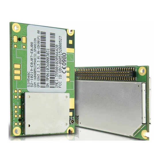
Page 90: Figure 49: Physical Sim548C
SIM548C Hardware Design The following figure is a top-view of SIM548C module. With the indication of Pin 1, 2, 59 and 60. Figure 49: physical SIM548C SIM548C_HD_V1.01 09.05.2008... -
Page 91: Appendix B: Reference Circuit With External Mcu (Gps Standalone Application)
SIM548C Hardware Design APPENDIX B: Reference Circuit with external MCU (GPS standalone application) Figure 50: Reference Circuit with external MCU (standalone application for example) SIM548C_HD_V1.01 09.05.2008... -
Page 92: Appendix C: Reference Diagram With External Mcu (Agps Application)
SIM548C Hardware Design APPENDIX C: Reference Diagram with external MCU (AGPS application) The next Figure shows the connection for AGPS application ,DISP_DATA pin is used for TX and DISP_D/C for RX. For details please refer to AGPS application note document. Figure 51 : AGPS connection ... - Page 93 Contact us: Shanghai SIMCom Wireless Solutions Ltd. Add: SIM Technology Building, No. 700, Yishan Road, Shanghai,P. R. China 200233 Tel: +86 21 5427 8900 Fax: +86 21 5427 6035 URL: www.sim.com/wm/...
Need help?
Do you have a question about the SIM548C HD V1.01 and is the answer not in the manual?
Questions and answers