Table of Contents
Advertisement
Quick Links
Download this manual
See also:
User Manual
C o m p a c t B o a r d
P C M - Q M 7 7
PCM-QM77
®
Intel
3rd Generation
TM
®
Core
i7/ i5/ i3/ Celeron
Processor
®
Intel
QM77/HM76 Chipset
10/100/1000Base-TX LANs
4 USB 3.0, 4 USB2.0, 10 COM
16-bit Digital I/O
2 SATA 6.0Gb/s (Optional RAID)
™
1 CFast
, 1 Mini Card, LPC
PCM-QM77 Manual 2
nd
Ed.
December 22, 2014
Advertisement
Table of Contents

Related Manuals for Aaeon PCM-QM77


Summary of Contents for Aaeon PCM-QM77
- Page 1 Celeron Processor ® Intel QM77/HM76 Chipset 10/100/1000Base-TX LANs 4 USB 3.0, 4 USB2.0, 10 COM 16-bit Digital I/O 2 SATA 6.0Gb/s (Optional RAID) ™ 1 CFast , 1 Mini Card, LPC PCM-QM77 Manual 2 December 22, 2014...
- Page 2 AAEON assumes no liabilities resulting from errors or omissions in this document, or from the use of the information contained herein. AAEON reserves the right to make changes in the product design without notice to its users.
- Page 3 C o m p a c t B o a r d P C M - Q M 7 7 Acknowledgments All other products’ name or trademarks are properties of their respective owners. AMI is a trademark of American Megatrends Inc. ...
- Page 4 17592QM772 Cooler DVD-ROM for Manual (in PDF Format) and Drivers PCM-QM77 1702150155 SATA cable 1709070500 SATA Power cable 9657666600 Jumper Cap If any of these items should be missing or damaged, please...
-
Page 5: Table Of Contents
C o m p a c t B o a r d P C M - Q M 7 7 Contents Chapter 1 General Information 1.1 Introduction..............1-2 1.2 Features ..............1-3 1.3 Specifications ............1-4 Chapter 2 Quick Installation Guide 2.1 Safety Precautions .......... - Page 6 C o m p a c t B o a r d P C M - Q M 7 7 2.15 AT/ATX Power Supply Mode Selection (JP8)..2-15 2.16 Front Panel Connector (JP9) ........ 2-16 2.17 Clear ME Jumper (JP10)........2-16 2.18 Clear CMOS Jumper (JP10) .........
- Page 7 C o m p a c t B o a r d P C M - Q M 7 7 2.40 LVDS Port 1 (CN21)..........2-39 2.41 LPC Port (CN22) ........... 2-41 2.42 COM Port 6 (CN23)..........2-42 2.36 COM Port 5 (CN24)..........2-44 2.37 PCI Slot (CN25).............
- Page 8 C o m p a c t B o a r d P C M - Q M 7 7 2.58 Touch Screen Connector (CN48)......2-59 2.59 CPU FAN Connector (CN49) ........ 2-61 2.60 UIM Card Connector (CN50)......... 2-61 2.61 Mini-Card Slot (CN51) ........... 2-62 2.62 CFast Slot (CN52) ..........
- Page 9 C o m p a c t B o a r d P C M - Q M 7 7 D.2 Setting AHCI ............D-8 Appendix E Electrical Specifications for I/O Ports E.1 Electrical Specifications for I/O Ports.....E-2 Appendix F Digital I/O F.1 Digital I/O ...............F-2 viii...
-
Page 10: Chapter 1 General Information
C o m p a c t B o a r d P C M - Q M 7 7 Chapter General Information 1- 1 Chapter 1 General Information... -
Page 11: Introduction
QM77/HM76 to offer high definition display function. In addition, it supports up to two 24-bit Dual-Channel LVDS, and one DVI. With all of its integrated features, the PCM-QM77 strikes a balance of performance and price. This versatile product targets Industrial Automation, Entertainment, Networking, KIOSK/POS, Transportation, Banking, Healthcare and Digital Signage applications that require high performance and high reliability. -
Page 12: Features
C o m p a c t B o a r d P C M - Q M 7 7 1.2 Features ® ® ® Intel 3rd Generation Intel Core™ i7/i5/i3/Celeron processor ® Intel QM77/HM76 204-pin DDR3 SODIMM x 2, DDR3/L 1333/1600, up to 16GB ... -
Page 13: Specifications
C o m p a c t B o a r d P C M - Q M 7 7 1.3 Specifications System From Factor 5.25” Compact Board (203 mm x 146 mm) ® ® ™ Processor Intel 3rd Generation Intel Core ®... - Page 14 C o m p a c t B o a r d P C M - Q M 7 7 Operating 32°F~140°F (0°C~60°C) Temperature Storage Temperature -40°F~176°F (-40°C~80°C) Operating Humidity 0% ~ 90% relative humidity, non-condensing Display: Supports CRT/LCD, DVI/LCD simultaneous / dual view displays ®...
- Page 15 C o m p a c t B o a r d P C M - Q M 7 7 Digital I/O 16-bit Programmable Audio Line-in, Line-out, Mic-in Chapter 1 General Information...
-
Page 16: Chapter 2 Quick Installation Guide
C o m p a c t B o a r d P C M - Q M 7 7 Chapter Quick Installation Guide Chapter 2 Quick Installation Guide... -
Page 17: Safety Precautions
C o m p a c t B o a r d P C M - Q M 7 7 2.1 Safety Precautions Always completely disconnect the power cord from your board whenever you are working on it. Do not make connections while the power is on, because a sudden rush of power can damage sensitive electronic components. -
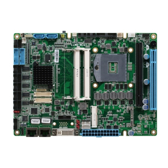
Page 18: Location Of Connectors And Jumpers
C o m p a c t B o a r d P C M - Q M 7 7 2.2 Location of Connectors and Jumpers Component Side Chapter 2 Quick Installation Guide... - Page 19 C o m p a c t B o a r d P C M - Q M 7 7 Solder Side Chapter 2 Quick Installation Guide...
-
Page 20: Mechanical Drawing
C o m p a c t B o a r d P C M - Q M 7 7 2.3 Mechanical Drawing Component Side Chapter 2 Quick Installation Guide... - Page 21 C o m p a c t B o a r d P C M - Q M 7 7 Solder Side Chapter 2 Quick Installation Guide...
-
Page 22: List Of Jumpers
C o m p a c t B o a r d P C M - Q M 7 7 2.4 List of Jumpers The board has a number of jumpers that allow you to configure your system to suit your application. The table below shows the function of each of the board's jumpers: Label Function... -
Page 23: List Of Connectors
C o m p a c t B o a r d P C M - Q M 7 7 2.5 List of Connectors The board has a number of connectors that allow you to configure your system to suit your application. The table below shows the function of each board's connectors: Label Function... - Page 24 C o m p a c t B o a r d P C M - Q M 7 7 CN20 COM Port 3 CN21 LVDS Port 1 CN22 LPC Port CN23 COM Port 6 CN24 COM Port 5 CN25 PCI Slot CN26 COM Port 8...
- Page 25 C o m p a c t B o a r d P C M - Q M 7 7 CN46 Digital IO Port 1 Connector CN47 Digital IO Port 2 Connector CN48 Touch Screen Connector (Optional) CN49 CPU Fan Connector CN50 UIM Card Connector CN51...
-
Page 26: Setting Jumpers
C o m p a c t B o a r d P C M - Q M 7 7 2.6 Setting Jumpers You configure your card to match the needs of your application by setting jumpers. A jumper is the simplest kind of electric switch. It consists of two metal pins and a small metal clip (often protected by a plastic cover) that slides over the pins to connect them. -
Page 27: Lvds Port 2 Operating Vdd Selection (Jp1)
C o m p a c t B o a r d P C M - Q M 7 7 2.7 LVDS Port 2 Operating VDD Selection (JP1) +3.3V (Default) Function +3.3V (Default) 2.8 LVDS Port 2 Backlight Inverter VCC Selection (JP1) +12V +5V (Default) Function... -
Page 28: Selection (Jp3)
C o m p a c t B o a r d P C M - Q M 7 7 Function VR Mode PWM Mode (Default) 2.10 LVDS Port 2 Backlight Lightness Control Mode Selection (JP3) 1 2 3 1 2 3 VR Mode PWM Mode (Default) Function... -
Page 29: Lvds Port 1 Backlight Inverter Vcc Selection (Jp4)
C o m p a c t B o a r d P C M - Q M 7 7 2.12 LVDS Port 1 Backlight Inverter VCC Selection (JP4) +12V +5V (Default) Function +12V +5V (Default) 2.13 COM6 Pin9 Function Selection (JP5) Ring(Default) +12V Function... -
Page 30: Com2 Pin9 Function Selection (Jp6)
C o m p a c t B o a r d P C M - Q M 7 7 2.14 COM2 Pin9 Function Selection (JP6) Ring(Default) +12V Function +12V Ring (Default) 2.15 AT/ATX Power Supply Mode Selection (JP8) 1 2 3 1 2 3 ATX Mode (Default) AT Mode... -
Page 31: Front Panel Connector (Jp9)
C o m p a c t B o a r d P C M - Q M 7 7 2.16 Front Panel Connector (JP9) Signal PWR_BTN- PWR_BTN+ HDD_LED- HDD_LED+ SPEAKER- SPEAKER+ PWR_LED- PWR_LED+ H/W RESET- H/W RESET+ 2.17 Clear ME Jumper (JP10) Normal (Default) Clear ME JP10... -
Page 32: Clear Cmos Jumper (Jp10)
C o m p a c t B o a r d P C M - Q M 7 7 Normal (Default) Clear ME Note: Clear ME need to use two jumper and be set after clear COMS. 2.18 Clear CMOS Jumper (JP10) Normal (Default) Clear CMOS JP10... - Page 33 C o m p a c t B o a r d P C M - Q M 7 7 Pin Name Signal Type Signal Level TMDS_DAT2+ DIFF TMDS_DAT2- DIFF DVI_DDC_CLK DVI_DDC_DATA VSYNC TMDS_DAT1- DIFF TMDS_DAT1+ DIFF TMDS_DAT3- DIFF TMDS_DAT3+ DIFF HPLG_DETECT TMDS_DAT0-...
-
Page 34: Stereo Audio Output Connector (Cn2)
C o m p a c t B o a r d P C M - Q M 7 7 TMDS_CLK+ DIFF TMDS_CLK- DIFF GREEN BLUE HSYNC GND_ANALOG 2.21 Stereo Audio Output Connector (CN2) PIN4 PIN3 PIN2 PIN1 Pin Name Signal Type Signal Level SPK_OUT_R+... -
Page 35: Ethernet#2 Connector (Cn3) (Optional)
C o m p a c t B o a r d P C M - Q M 7 7 2.22 Ethernet#2 Connector (CN3) (Optional) MDI0+ MDI0- MDI1+ MDI1- MDI2+ MDI2- MDI3+ MDI3- Pin Name Signal Type Signal Level DIFF MDI0+ DIFF MDI0-... -
Page 36: Ethernet#2 Connector (Cn5)
C o m p a c t B o a r d P C M - Q M 7 7 Pin Name Signal Type Signal Level DIFF MDI0+ DIFF MDI0- DIFF MDI1+ DIFF MDI1- DIFF MDI2+ DIFF MDI2- DIFF MDI3+ DIFF MDI3- 2.24 RJ-45 Ethernet#2 Connector (CN5) -
Page 37: Ethernet#1 Connector (Cn6)
C o m p a c t B o a r d P C M - Q M 7 7 DIFF MDI2+ DIFF MDI2- DIFF MDI1- DIFF MDI3+ DIFF MDI3- 2.25 RJ-45 Ethernet#1 Connector (CN6) Pin Name Signal Type Signal Level DIFF MDI0+ DIFF... -
Page 38: Atx Power Connector (Cn7)
C o m p a c t B o a r d P C M - Q M 7 7 2.26 ATX Power Connector (CN7) PIN1 PIN12 PIN13 PIN24 Pin Name Signal Type Signal Level +3.3V +3.3V +3.3V +3.3V PWR_OK +5VSB +12V +12V... -
Page 39: Lvds Port 2 Inverter / Backlight Connector (Cn8)2-24
C o m p a c t B o a r d P C M - Q M 7 7 PS_ON# 2.27 LVDS Port 2 Inverter / Backlight Connector (CN8) BLK_PWR BKL_CONTROL BKL_ENABLE Pin Name Signal Type Signal Level BKL_PWR +5V / +12V BKL_CONTROL BKL_ENABLE... -
Page 40: Lvds Port 1 Inverter / Backlight Connector (Cn9)2-25
C o m p a c t B o a r d P C M - Q M 7 7 2.28 LVDS Port 1 Inverter / Backlight Connector (CN9) BLK_PWR BKL_CONTROL BKL_ENABLE Pin Name Signal Type Signal Level BKL_PWR +5V / +12V BKL_CONTROL BKL_ENABLE Note: LVDS1 BKL_PWR can be set to +5V or +12V by JP4. -
Page 41: D-Sub Crt Connector (Cn11) (Optional)
C o m p a c t B o a r d P C M - Q M 7 7 MIC_L GND_AUDIO CD_GND LINE_L_IN CD_L LINE_R_IN CD_GND GND_AUDIO CD_R LEFT_OUT RIGHT_OUT GND_AUDIO GND_AUDIO 2.30 D-SUB CRT Connector (CN11) (Optional) Pin Name Signal Type Signal Level GREEN... -
Page 42: Crt Connector (Cn12)
C o m p a c t B o a r d P C M - Q M 7 7 RED_GND_RTN GREEN_GND_RTN BLUE_GND_RTN DDC_DATA HSYNC VSYNC DDC_CLK 2.31 CRT Connector (CN12) GREEN BLUE DDC_DATA HSYNC VSYNC CRT_PLUG# DDC_CLK Pin Name Signal Type Signal Level 2-27... -
Page 43: Msata Slot (Cn13)
C o m p a c t B o a r d P C M - Q M 7 7 GREEN BLUE DDC_DATA HSYNC VSYNC DDC_CLK 2.32 mSATA Slot (CN13) Pin Name Signal Type Signal Level +3.3V +3.3V 2-28 Chapter 2 Quick Installation Guide... - Page 44 C o m p a c t B o a r d P C M - Q M 7 7 +1.5V +1.5V SATA_TX+ DIFF +3.3V +3.3V 2-29 Chapter 2 Quick Installation Guide...
- Page 45 C o m p a c t B o a r d P C M - Q M 7 7 SATA_TX- DIFF +1.5V +1.5V SMB_CLK +3.3V SATA_RX- DIFF SMB_DATA +3.3V SATA_RX+ DIFF +3.3V +3.3V +3.3V +3.3V 2-30 Chapter 2 Quick Installation Guide...
-
Page 46: Ethernet#1 Led Indicator (Cn14)
C o m p a c t B o a r d P C M - Q M 7 7 +1.5V +1.5V +3.3V +3.3V 2.33 Ethernet#1 LED Indicator (CN14) PIN1 PIN2 PIN3 PIN4 PIN5 PIN6 Pin Name Signal Type Signal Level ACT_LED+ ACT_LED- 100_LED+... -
Page 47: Com Port 2 (Cn15)
C o m p a c t B o a r d P C M - Q M 7 7 2.34 COM Port 2 (CN15) RI/+5V/+12V RS-232 Pin Name Signal Type Signal Level ±5V ±5V ±5V RI/+5V/+12V IN/ PWR +5V/+12V RS485_D- RS485_D+ NC/+5V/+12V... - Page 48 C o m p a c t B o a r d P C M - Q M 7 7 Pin Name Signal Type Signal Level RS485_D- ±5V RS485_D+ ±5V NC/+5V/+12V +5V/+12V RS422_TX- RS422_TX+ RS422_RX+ RS422_RX- NC/+5V/+12V RS-422 Pin Name Signal Type Signal Level RS422_TX-...
-
Page 49: Com Port 1 (Cn16)
C o m p a c t B o a r d P C M - Q M 7 7 NC/+5V/+12V +5V/+12V Note: COM2 RS-232/422/485 can be set by BIOS setting. Default is RS-232. COM2 Pin 9 function can be set by JP6. 2.35 COM Port 1 (CN16) Pin Name Signal Type... -
Page 50: Ethernet#2 Led Indicator (Cn17)
C o m p a c t B o a r d P C M - Q M 7 7 2.36 Ethernet#2 LED Indicator (CN17) PIN1 PIN2 PIN3 PIN4 PIN5 PIN6 Pin Name Signal Type Signal Level ACT_LED+ ACT_LED- 100_LED+ 100_LED- 1000_LED+ 1000_LED-... - Page 51 C o m p a c t B o a r d P C M - Q M 7 7 BKL_CONTROL LCD_PWR +3.3V/+5V LVDS_A_CLK- DIFF LVDS_A_CLK+ DIFF LCD_PWR +3.3V/+5V LVDS_DA0- DIFF LVDS_DA0+ DIFF LVDS_DA1- DIFF LVDS_DA1+ DIFF LVDS_DA2- DIFF LVDS_DA2+ DIFF LVDS_DA3- DIFF...
-
Page 52: Com Port 4 (Cn19)
C o m p a c t B o a r d P C M - Q M 7 7 LVDS_DB1+ DIFF LVDS_DB2- DIFF LVDS_DB2+ DIFF LVDS_DB3- DIFF LVDS_DB3+ DIFF LCD_PWR +3.3V/+5V LVDS_B_CLK- DIFF LVDS_B_CLK+ DIFF 2.38 COM Port 4 (CN19) Pin Name Signal Type Signal Level... -
Page 53: Com Port 3 (Cn20)
C o m p a c t B o a r d P C M - Q M 7 7 ±9V 2.39 COM Port 3 (CN20) Pin Name Signal Type Signal Level ±9V ±9V ±9V 2-38 Chapter 2 Quick Installation Guide... -
Page 54: Lvds Port 1 (Cn21)
C o m p a c t B o a r d P C M - Q M 7 7 2.40 LVDS Port 1 (CN21) PIN 29 PIN 30 PIN 1 PIN 2 Pin Name Signal Type Signal Level BKL_ENABLE BKL_CONTROL LCD_PWR +3.3V/+5V... - Page 55 C o m p a c t B o a r d P C M - Q M 7 7 LVDS_DA1+ DIFF LVDS_DA2- DIFF LVDS_DA2+ DIFF LVDS_DA3- DIFF LVDS_DA3+ DIFF DDC_DATA +3.3V DDC_CLK +3.3V LVDS_DB0- DIFF LVDS_DB0+ DIFF LVDS_DB1- DIFF LVDS_DB1+ DIFF LVDS_DB2-...
-
Page 56: Lpc Port (Cn22)
C o m p a c t B o a r d P C M - Q M 7 7 2.41 LPC Port (CN22) LAD0 LAD1 LAD2 LAD3 +3.3V LFRAME# LRESET# LCLK LDRQ0 LDRQ1 SERIRQ Pin Name Signal Type Signal Level +3.3V LAD0 +3.3V... -
Page 57: Com Port 6 (Cn23)
C o m p a c t B o a r d P C M - Q M 7 7 2.42 COM Port 6 (CN23) RI/+5V/+12V RS-232 Pin Name Signal Type Signal Level ±5V ±5V ±5V RI/+5V/+12V IN/ PWR +5V/+12V RS485_D- RS485_D+ NC/+5V/+12V... - Page 58 C o m p a c t B o a r d P C M - Q M 7 7 Pin Name Signal Type Signal Level RS485_D- ±5V RS485_D+ ±5V NC/+5V/+12V +5V/+12V RS422_TX- RS422_TX+ RS422_RX+ RS422_RX- NC/+5V/+12V RS-422 Pin Name Signal Type Signal Level RS422_TX-...
-
Page 59: Com Port 5 (Cn24)
C o m p a c t B o a r d P C M - Q M 7 7 NC/+5V/+12V +5V/+12V Note: 1. COM6 RS-232/422/485 can be set by BIOS setting. Default is RS-232. 2. COM6 Pin 9 function can be set by JP5. 3. -
Page 60: Pci Slot (Cn25)
C o m p a c t B o a r d P C M - Q M 7 7 2.37 PCI Slot (CN25) Standard specification 2.38 COM Port 8 (CN26) Pin Name Signal Type Signal Level ±9V ±9V ±9V 2-45 Chapter 2 Quick Installation Guide... -
Page 61: Com Port 7 (Cn27)
C o m p a c t B o a r d P C M - Q M 7 7 2.39 COM Port 7 (CN27) Pin Name Signal Type Signal Level ±9V ±9V ±9V 2.40 PCI-Express[x16]Slot (CN28) Standard specification 2.41 DDR3 SO-DIMM Channel B Slot (CN29) Standard specification 2.42 DDR3 SO-DIMM Channel A Slot (CN30) Standard specification... -
Page 62: Com Port 10 (Cn31)
C o m p a c t B o a r d P C M - Q M 7 7 2.43 COM Port 10 (CN31) Pin Name Signal Type Signal Level ±9V ±9V ±9V 2.44 COM Port 9 (CN32) Pin Name Signal Type Signal Level 2-47... -
Page 63: Usb 3.0 Ports 1 And 2 (Cn34)
C o m p a c t B o a r d P C M - Q M 7 7 ±9V ±9V ±9V 2.45 USB 3.0 Ports 1 and 2 (CN34) PIN1 PIN19 PIN11 PIN10 Pin Name Signal Type Signal Level +5VSB USB1_SSRX−... - Page 64 C o m p a c t B o a r d P C M - Q M 7 7 USB1_SSTX− DIFF USB1_SSTX+ DIFF USB1_D- DIFF USB1_D+ DIFF USB2_D+ DIFF USB2_D- DIFF USB2_SSTX+ DIFF USB2_SSTX− DIFF USB2_SSRX+ DIFF USB2_SSRX− DIFF +5VSB 2-49 Chapter 2 Quick Installation Guide...
-
Page 65: Usb 3.0 Ports 3 And 4 (Cn35)
C o m p a c t B o a r d P C M - Q M 7 7 2.46 USB 3.0 Ports 3 and 4 (CN35) PIN1 PIN19 PIN11 PIN10 Pin Name Signal Type Signal Level +5VSB USB3_SSRX− DIFF USB3_SSRX+ DIFF... -
Page 66: Usb 2.0 Ports 5 And 6 (Cn36)
C o m p a c t B o a r d P C M - Q M 7 7 USB4_SSTX− DIFF USB4_SSRX+ DIFF USB4_SSRX− DIFF +5VSB 2.47 USB 2.0 Ports 5 and 6 (CN36) +5VSB USB5_D- USB5_D+ USB6_D+ USB6_D- +5VSB Pin Name Signal Type... -
Page 67: Usb 2.0 Ports 7 And 8 (Cn37)
C o m p a c t B o a r d P C M - Q M 7 7 2.48 USB 2.0 Ports 7 and 8 (CN37) +5VSB USB7_D- USB7_D+ USB8_D+ USB8_D- +5VSB Pin Name Signal Type Signal Level +5VSB USB7_D- DIFF... -
Page 68: Irda Connector (Cn39) (Optional)
C o m p a c t B o a r d P C M - Q M 7 7 Pin Name Signal Type Signal Level KB_ DATA KB_CLK +5VSB MS_DATA MS_CLK 2.50 IrDA Connector (CN39) (Optional) IRRX IRTX Pin Name Signal Type Signal Level IRRX... -
Page 69: Sata Port 2 Connector (Cn40)
C o m p a c t B o a r d P C M - Q M 7 7 2.51 SATA Port 2 Connector (CN40) Pin 1 Pin 7 Pin Name Signal Type Signal Level SATA_TX+ DIFF SATA_TX- DIFF SATA_RX- DIFF SATA_RX+... -
Page 70: Output For Sata Hdd (Cn43)
C o m p a c t B o a r d P C M - Q M 7 7 SATA_TX- DIFF SATA_RX- DIFF SATA_RX+ DIFF 2.53 +5V Output for SATA HDD (CN43) Pin Name Signal Type Signal Level 2.54 LPT Connector (CN44) STROBE# AFD# ERROR#... - Page 71 C o m p a c t B o a r d P C M - Q M 7 7 STROBE# AFD# ERROR# PRINT# SLIN# ACK# 2-56 Chapter 2 Quick Installation Guide...
-
Page 72: System Fan Connector (Cn45)
C o m p a c t B o a r d P C M - Q M 7 7 BUSY SLCT 2.55 System Fan Connector (CN45) FAN_TAC FAN_POWER Pin Name Signal Type Signal Level +12V FAN_POWER FAN_TAC 2.56 Digital IO Port 1 Connector (CN46) 2-57 Chapter 2 Quick Installation Guide... -
Page 73: Digital Io Port 2 Connector (Cn47)
C o m p a c t B o a r d P C M - Q M 7 7 DIO0 DIO1 DIO2 DIO3 DIO4 DIO5 DIO6 DIO7 Pin Name Signal Type Signal Level DIO0 DIO1 DIO2 DIO3 DIO4 DIO5 DIO6 DIO7 2.57 Digital IO Port 2 Connector (CN47) -
Page 74: P C M - Q
C o m p a c t B o a r d P C M - Q M 7 7 Pin Name Signal Type Signal Level DIO0 DIO1 DIO2 DIO3 DIO4 DIO5 DIO6 DIO7 2.58 Touch Screen Connector (CN48) (Optional) 4-wire 4 Wires BOTTOM... - Page 75 C o m p a c t B o a r d P C M - Q M 7 7 BOTTOM LEFT RIGHT 5-wire 5 Wires UL(Y) UR(H) LL(L) LR(X) SENSE(S) Pin Name Signal Type Signal Level UL(Y) UR(H) LL(L) 2-60 Chapter 2 Quick Installation Guide...
-
Page 76: Cpu Fan Connector (Cn49)
C o m p a c t B o a r d P C M - Q M 7 7 LR(X) SENSE(S) Note: Touch mode can be set by JP11 2.59 CPU FAN Connector (CN49) FAN_TAC FAN_POWER FAN_CTL Pin Name Signal Type Signal Level +12V... -
Page 77: Mini-Card Slot (Cn51)
C o m p a c t B o a r d P C M - Q M 7 7 Pin Name Signal Type Signal Level UIM_PWR UIM_RST UIM_CLK UIM_VPP UIM_DATA 2.61 Mini-Card Slot (CN51) Pin Name Signal Type Signal Level PCIE_WAKE# +3.3V +3.3VSB... - Page 78 C o m p a c t B o a r d P C M - Q M 7 7 UIM_CLK PCIE_REF_CLK+ DIFF UIM_RST UIM_VPP W_DISABLE# +3.3V PCIE_RST# +3.3V PCIE_RX- DIFF +3.3VSB +3.3V PCIE_RX+ DIFF +1.5V +1.5V SMB_CLK +3.3V PCIE_TX- DIFF 2-63 Chapter 2 Quick Installation Guide...
- Page 79 C o m p a c t B o a r d P C M - Q M 7 7 SMB_DATA +3.3V PCIE_TX+ DIFF USB_D- DIFF USB_D+ DIFF +3.3VSB +3.3V +3.3VSB +3.3V +1.5V +1.5V 2-64 Chapter 2 Quick Installation Guide...
-
Page 80: Cfast Slot (Cn52)
C o m p a c t B o a r d P C M - Q M 7 7 +3.3VSB +3.3V 2.62 CFast Slot (CN52) Pin Name Signal Type Signal Level DIFF SATA_TX+ DIFF SATA_TX- DIFF SATA_RX- DIFF SATA_RX+ 2-65 Chapter 2 Quick Installation Guide... - Page 81 C o m p a c t B o a r d P C M - Q M 7 7 PC10 PC11 PC12 +3.3V PC13 +3.3V +3.3V PC14 +3.3V PC15 PC16 PC17 2-66 Chapter 2 Quick Installation Guide...
- Page 82 C o m p a c t B o a r d P C M - Q M 7 7 Below Table for China RoHS Requirements 产品中有毒有害物质或元素名称及含量 AAEON Main Board/ Daughter Board/ Backplane 有毒有害物质或元素 部件名称 铅 汞 镉 六价铬 多溴联苯...
-
Page 83: Chapter 3 Ami Bios Setup
C o m p a c t B o a r d P C M - Q M 7 7 Chapter BIOS Setup Chapter 3 AMI BIOS Setup 3-1... -
Page 84: System Test And Initialization
3. The CMOS memory has lost power and the configuration information has been erased. The PCM-QM77 CMOS memory has an integral lithium battery backup for data retention. However, you will need to replace the complete unit when it finally runs down. -
Page 85: Ami Bios Setup
C o m p a c t B o a r d P C M - Q M 7 7 3.2 AMI BIOS Setup AMI BIOS ROM has a built-in Setup program that allows users to modify the basic system configuration. This type of information is stored in battery-backed CMOS RAM so that it retains the Setup information when the power is turned off. - Page 86 C o m p a c t B o a r d P C M - Q M 7 7 Setup Menu Setup submenu: Main Options summary: (default setting) System Date Day MM:DD:YYYY Change the month, year and century. The ‘Day’ is changed automatically. System Time HH : MM : SS Change the clock of the system.
- Page 87 ICC Spread Spectrum Disabled Enabled Spread Spectrum Support AAEON ICC Spread Spectrum AAEON ICC Spread Spectrum default value ACPI Settings System ACPI Parameters S5 RTC Wake Settings Enable system to wake from S5 using RTC alarm. Chapter 3 AMI BIOS Setup 3-5...
- Page 88 C o m p a c t B o a r d P C M - Q M 7 7 Trusted Computing Trusted Computing Settings CPU Configuration CPU Configuration Parameters Dynamic Digital IO Configuration DIO setting SATA Configuration SATA Device Options Settings Intel TXT(LT) Configuration Intel Trusted Execution Technology...
- Page 89 C o m p a c t B o a r d P C M - Q M 7 7 ACPI Settings Options summary: (default setting) Suspend Disabled S1 only(CPU Stop Clock) ACPI Sleep State S3 only(Suspend to RAM) Both S1 and S3 available for OS to choose from Select the ACPI state used for System Suspend Chapter 3 AMI BIOS Setup 3-7...
- Page 90 C o m p a c t B o a r d P C M - Q M 7 7 RTC Wake Settings Options summary: (default setting) Wake system with Fixed Disabled Time Enabled Enable or disable System wake on alarm event. Wake up time is setting by following settings.
- Page 91 C o m p a c t B o a r d P C M - Q M 7 7 Wake up minute 0-59 Wake up second 0-59 Wake system with Disabled Dynamic Time Enabled Enable or disable System wake on alarm event. Wake up time is current time + Increase minutes.
- Page 92 C o m p a c t B o a r d P C M - Q M 7 7 Trusted Computing Options summary: (default setting) Security Device Support Disabled Enabled En/Disable TPM support. TPM State Disabled Enabled En/Disable TPM functionality. Pending TPM Operation None Enable Take Ownership...
- Page 93 C o m p a c t B o a r d P C M - Q M 7 7 CPU Configuration Options summary: (default setting) Hyper-Threading Disabled Enabled En/Disable CPU Hyper-Threading function Active Processor Cores 1 to Max CPU cores Number of CPU cores to be active.
- Page 94 C o m p a c t B o a r d P C M - Q M 7 7 Dynamic Digital IO Configration Options summary: (default setting) Digital Port X(GPXX) Input Direction Output Set GPIOx as Input or Output Digital Port X(GPXX) Levels Set GPIO output level when used as output pin Chapter 3 AMI BIOS Setup 3-12...
- Page 95 C o m p a c t B o a r d P C M - Q M 7 7 SATA Configuration Options summary: (default setting) SATA Controller(s) Disabled Enabled En/Disable SATA controller Configure SATA as AHCI RAID Configure SATA controller operating as IDE/AHCI/RAID mode. SATA Controller Speed Gen1 Gen2...
- Page 96 C o m p a c t B o a r d P C M - Q M 7 7 Port X Disabled Enabled En/Disable the selected port. Hot Plug Disabled Enabled En/Disable Hot Plug feature for specified port. Intel TXT (LT) Configuration Options summary: (default setting) Intel TXT(LT) Support Disabled...
- Page 97 C o m p a c t B o a r d P C M - Q M 7 7 AMT Configuration Options summary: (default setting) Intel AMT Enabled Disabled En/Disable Intel® Active Management Technology BIOS Extension. Note: iAMT H/W is always enabled. This option just controls the BIOS extension execution.
- Page 98 C o m p a c t B o a r d P C M - Q M 7 7 USB Configuration Options summary: (default setting) Legacy USB Support Enabled Disabled Auto Enables BIOS Support for Legacy USB Support. When enabled, USB can be functional in legacy environment like DOS.
- Page 99 C o m p a c t B o a r d P C M - Q M 7 7 Enables BIOS Support for USB3.0 (XHCI). When disabled, PCH USB3.0 controller will also be disabled. Device Name Auto (Emulation Type) Floppy Forced FDD Hard Disk...
- Page 100 C o m p a c t B o a r d P C M - Q M 7 7 F81216 Second Super IO Configuration Options summary: (default setting) Serial Port 7/8/9/10 Configuration Set Parameters of Serial Port 7/8/9/10 Chapter 3 AMI BIOS Setup 3-18...
- Page 101 C o m p a c t B o a r d P C M - Q M 7 7 F81866 Super IO Configutation Options summary: (default setting) Serial Port 1/2/3/4/5/6 Configuration Set Parameters of Serial Port 1/2/3/4/5/6 Parallel Port Configuration Set Parameters of Parallel Port.
- Page 102 C o m p a c t B o a r d P C M - Q M 7 7 Serial Port X Configuration Options summary: (default setting) Serial Port Disabled Enabled En/Disable specified serial port. Change Settings Auto IO=2F8h; IRQ=3; IO=3F8h;...
- Page 103 C o m p a c t B o a r d P C M - Q M 7 7 Select a resource setting for Super IO device. Device Type RS232 RS422 RS485 Configure COM2/6 operated as RS232, RS422 or RS485. Parallel Port Configuration Options summary: (default setting) Parallel Port...
- Page 104 C o m p a c t B o a r d P C M - Q M 7 7 Change Settings Auto IO=378h; IRQ=7; IO=378h; IRQ=5,7,10,11,12; IO=278h; IRQ=5,7,10,11,12; IO=3BCh; IRQ=5,7,10,11,12; Select a resource setting for Super IO device. Device Mode STD Printer Mode SPP Mode EPP-1.9 and SPP Mode...
- Page 105 C o m p a c t B o a r d P C M - Q M 7 7 F81866 H/W Monitor Options summary: (default setting) Smart Fan Function Disabled Enabled Enable or Disable Smart Fan Smart Fan Mode configuration Smart Fan Mode select Chapter 3 AMI BIOS Setup 3-23...
- Page 106 C o m p a c t B o a r d P C M - Q M 7 7 Smart Fan Mode configuration Options summary: (default setting) Fan 1/2 Smart Fan Control Manual Duty Mode Auto Duty-Cycle Mode Manual Duty Mode: Manually controlling the fan with a given control PWM. Auto Duty-Cycle Mode: Automatically controlling the fan with given parameters.
- Page 107 C o m p a c t B o a r d P C M - Q M 7 7 Duty Cycle 0/1/2/3/4 1 to 100, default is 100/85/70/60/50 Auto fan speed control. Fan speed will follow different temperature by different duty cycle 1-100 CPU PPM Configuration Options summary: (default setting)
- Page 108 C o m p a c t B o a r d P C M - Q M 7 7 Setup submenu: Chipset Options summary: (default setting) PCH-IO Configuration South Bridge Parameters System Agent (SA) Configuration SA Parameters Chapter 3 AMI BIOS Setup 3-26...
- Page 109 C o m p a c t B o a r d P C M - Q M 7 7 PCH-IO Configuration Options summary: (default setting) Power Mode ATX Type AT Type Enable or disable ‘It is now safe to turn off your computer.’ string PCI Express Configuration PCI Express Configuration settings...
- Page 110 C o m p a c t B o a r d P C M - Q M 7 7 82583V LAN Controller Enabled Disabled En/Disabled Intel 82583V NIC PCH LAN Controller Enabled Disabled En/Disabled onboard NIC Wake on LAN Enabled Disabled En/Disabled integrated LAN to wake the system.
- Page 111 C o m p a c t B o a r d P C M - Q M 7 7 System Agent (SA) Configuration Options summary: (default setting) VT-d Disabled Enabled Check to enable VT-d function on MCH Graphics Configuration Config Graphics Settings Chapter 3 AMI BIOS Setup 3-29...
- Page 112 C o m p a c t B o a r d P C M - Q M 7 7 Graphics Configuration Options summary: (default setting) Primary Display Auto IGFX Select graphic adapters to boot Internal Graphics Auto Disabled Enabled En/Disabled internal graphics device Chapter 3 AMI BIOS Setup 3-30...
- Page 113 C o m p a c t B o a r d P C M - Q M 7 7 DVMT Pre-Allocated 64MB 32MB~1024MB Select DVMT 5.0 Pre-Allocated (Fixed) Graphics Memory size used by the Internal Graphics Device. DVMT Total Gfx Mem 128MB 256MB Select DVMT 5.0 Total Graphic Memory size used by the Internal Graphics Device.
- Page 114 C o m p a c t B o a r d P C M - Q M 7 7 LCD Control Options summary: (default setting) Primary IGFX Boot Display VBIOS LVDS LVDS2 CRT+LVDS1 Select Primary IGFX boot display device LVDS1 Control Disabled Enabled...
- Page 115 C o m p a c t B o a r d P C M - Q M 7 7 Enable or Disable Internal LVDS LVDS2 Control Disabled Enabled Enable or Disable Onboard CH7511 LVDS1/LVDS2 Panel Type 640x480,18-Bit,60Hz 800x480,18-Bit,60Hz 800x600,18-Bit,60Hz 1024x600,18-Bit,60Hz 1024x768,18-Bit,60Hz 1024x768,24-Bit,60Hz...
- Page 116 C o m p a c t B o a r d P C M - Q M 7 7 Select Backlight control type. Inverted: Brightest for low PWM duty cycle and low voltage. Normal: Brightest for high PWM duty cycle and high voltage. LVDS1/LVDS2 Backlight 100% Level...
- Page 117 C o m p a c t B o a r d P C M - Q M 7 7 Setup submenu: Boot Options summary: (default setting) Quiet Boot Disabled Enabled En/Disable showing boot logo. Launch PXE OpROM Disabled policy Enabled En/Disable PXE boot for LAN Boot Option #X/...
- Page 118 C o m p a c t B o a r d P C M - Q M 7 7 BBS Priorities Options summary: (default setting) Boot Option #x Disabled Device name Sets the system boot order Chapter 3 AMI BIOS Setup 3-36...
- Page 119 C o m p a c t B o a r d P C M - Q M 7 7 Setup submenu: Security Options summary: (default setting) Administrator Password/ Not set User Password Chapter 3 AMI BIOS Setup 3-37...
- Page 120 C o m p a c t B o a r d P C M - Q M 7 7 You can install a Supervisor password, and if you install a supervisor password, you can then install a user password. A user password does not provide access to many of the features in the Setup utility.
- Page 121 C o m p a c t B o a r d P C M - Q M 7 7 Setup submenu: Exit Options summary: (default setting) Save Changes and Exit Exit system setup after saving the changes Discard Changes and Exit Exit system setup without saving any changes Save Changes and Reset Reset the system after saving the changes...
- Page 122 C o m p a c t B o a r d P C M - Q M 7 7 Discard Changes Discard Changes done so far to any of the setup options Reset system setup without saving any changes Restore Defaults Restore/Load Default values for all the setup options.
-
Page 123: Chapter 4 Driver Installation
C o m p a c t B o a r d P C M - Q M 7 7 Chapter Driver Installation 4 -1 Chapter 4 Driver Installation... - Page 124 C o m p a c t B o a r d P C M - Q M 7 7 The PCM-QM77 comes with an AutoRun DVD-ROM that contains all drivers and utilities that can help you to install the driver automatically.
- Page 125 C o m p a c t B o a r d P C M - Q M 7 7 4.1 Installation: Insert the PCM-QM77 DVD-ROM into the DVD-ROM drive. And install the drivers from Step 1 to Step 10 in order. Step 1 – Install Chipset Driver 1.
- Page 126 C o m p a c t B o a r d P C M - Q M 7 7 ® Note 2: If the OS is Windows XP, you have to install the driver of dotNet Framework first. Simply click on dotnetfx35.exe located in dotNet Framwork folder.
- Page 127 C o m p a c t B o a r d P C M - Q M 7 7 Step 6 –Install RAID & AHDI Driver Please refer to the Appendix D RAID & AHDI Settings Step 7 – Install TPM Driver 1.
- Page 128 C o m p a c t B o a r d P C M - Q M 7 7 Step 10 – Install Serial Port Driver (Optional) ® For Windows 1. Click on the STEP10-Serial Port Driver (Optional) and select the Windows XP OS version folder (WINXP_32 or WWINXP_64) your system is 2.
- Page 129 C o m p a c t B o a r d P C M - Q M 7 7 2. Change User Account Control Settings to [Never notify] 3. Reboot and Administrator login. 4 -7 Chapter 4 Driver Installation...
- Page 130 C o m p a c t B o a r d P C M - Q M 7 7 4. To run patch.bat with [Run as administrator]. 4 -8 Chapter 4 Driver Installation...
-
Page 131: Appendix A Programming The Watchdog Timer
C o m p a c t B o a r d P C M - Q M 7 7 Appendix Programming the Watchdog Timer Appendix A Programming the Watchdog Timer... -
Page 132: Programming
C o m p a c t B o a r d P C M - Q M 7 7 A.1 Programming PCM-QM77 utilizes FINTEK 81866 chipset as its watchdog timer controller. Below are the procedures to complete its configuration and the AAEON initial watchdog timer program is also attached based on which you can develop customized program to fit your application. - Page 133 C o m p a c t B o a r d P C M - Q M 7 7 There are three steps to complete the configuration setup: (1) Enter the MB PnP Mode; (2) Modify the data of configuration registers; (3) Exit the MB PnP Mode.
- Page 134 C o m p a c t B o a r d P C M - Q M 7 7 Watch Dog Timer 1, 2, 3 Control Register (Index=F5h,F6h,FAh Default=00h) Appendix A Programming the Watchdog Timer...
-
Page 135: F81866 Watchdog Timer Initial Program
C o m p a c t B o a r d P C M - Q M 7 7 A.2 F81866 Watchdog Timer Initial Program Main (){ aaeonSuperIOOpen(); aaeonWdtSetCountMode(BOOL bMinute); // Set wdt count mode aaeonWdtSetTimeoutCount(BYTE tTimeout); // Set wdt timer aaeonWdtSetEnable(BOOL bEnable); // Enable wdt aaeonSuperIOClose(); } Void aaeonSuperIOOpen(){ // Config F81866 Entry key aaeonioWritePortByte(F81866_INDEX, 0x87); aaeonioWritePortByte(F81866_INDEX, 0x87); ... - Page 136 C o m p a c t B o a r d P C M - Q M 7 7 Void aaeonWdtSetTimeoutCount(BYTE tTimeout){ f81866SetLdn(0x07); f81866WriteByte(F81866_WDT_TIME_REG, tTimeout); } Void aaeonWdtSetEnable(BOOL bEnable){ f81866SetLdn(0x07); if(bEnable){ f81866WriteByte(0x30, 0x01); WDT_BASE_ADDR = (f81866ReadByte(F81866_WDT_BASEADDR_REG_MSB) << 8) ...
- Page 137 C o m p a c t B o a r d P C M - Q M 7 7 Void aaeonSuperIOClose(){ aaeonioWritePortByte(F81866_INDEX, 0xaa); } Appendix A Programming the Watchdog Timer...
-
Page 138: Appendix B I/O Information
C o m p a c t B o a r d P C M - Q M 7 7 Appendix I/O Information Appendix B I/O Information... -
Page 139: I/O Address Map
C o m p a c t B o a r d P C M - Q M 7 7 B.1 I/O Address Map Appendix B I/O Information... -
Page 140: Memory Address Map
C o m p a c t B o a r d P C M - Q M 7 7 B.2 Memory Address Map Appendix B I/O Information... -
Page 141: Irq Mapping Chart
C o m p a c t B o a r d P C M - Q M 7 7 B.3 IRQ Mapping Chart Appendix B I/O Information... -
Page 142: Dma Channel Assignments
C o m p a c t B o a r d P C M - Q M 7 7 B.4 DMA Channel Assignments Appendix B I/O Information... -
Page 143: Appendix C Mating Connector
C o m p a c t B o a r d P C M - Q M 7 7 Appendix Mating Connector C - 1 Appendix C Mating Connector... -
Page 144: List Of Mating Connectors And Cables
Connector COM Port 3 CN20 Molex 51110-1050 Serial Port 1701100206 Connector LVDS#1 DF13-30DS- CN21 HIROSE Connector 1.25C SHR-12V-S- AAEON LPC CN22 LPC Port 1703120130 Cable COM Port 6 CN23 Molex 51110-1050 Serial Port 1701100206 Connector COM Port 5 CN24 Molex... - Page 145 C o m p a c t B o a r d P C M - Q M 7 7 Connector COM Port 9 CN32 Molex 51110-1050 Serial Port 1701100206 Connector USB 3.0 Port #1, UB210 CN34 HO-BASE USB 3.0 Cable 1700200401 #2 Connector FB-1T1...
- Page 146 C o m p a c t B o a r d P C M - Q M 7 7 A ppendix RAID & AHCI Settings Appendix D RAID & AHCI Settings...
- Page 147 C o m p a c t B o a r d P C M - Q M 7 7 D.1 Setting RAID OS installation to SETUP RAID Mode Step 1: Extract the f6fly-x86.zip from “Driver CD -> Step7-RAID&AHCI\WinXP_32” and copy below files to diskette. Step 2: Connect the USB Floppy drive to the board and insert the diskette from previous step.
- Page 148 C o m p a c t B o a r d P C M - Q M 7 7 Step 4: Configure DVD/CD-ROM drive as the first boot device. Step 5: Save changes and exit BIOS SETUP Appendix D RAID & AHCI Settings...
- Page 149 C o m p a c t B o a r d P C M - Q M 7 7 Step 6: Press CTRL-I to enter RAID Configuration Utility Step 7: Choose “1. Create RAID Volume” Appendix D RAID & AHCI Settings...
- Page 150 C o m p a c t B o a r d P C M - Q M 7 7 Step 8 – Configure RAID parameters for the system Step 9 – Choose “Create Volume” and confirmed in next warning message.
- Page 151 C o m p a c t B o a r d P C M - Q M 7 7 Step 10 – Exit RAID Configuration Utility and Reboot to DVD/CD-ROM device to install OS Step 11 – Press “F6” to install RAID driver Appendix D RAID &...
-
Page 152: Appendix D Raid & Ahci Settings
C o m p a c t B o a r d P C M - Q M 7 7 Step 12 – Press “S” to install RAID driver Step 13 – Choose “Intel(R) Mobile Express Chipset SATA RAID Controller” Appendix D RAID &... -
Page 153: D.2 Setting Ahci
C o m p a c t B o a r d P C M - Q M 7 7 Step 14 – It will show the model you selected and then press ”ENTER”. Windows Setup will continue to install OS. D.2 Setting AHCI OS installation to SETUP AHCI Mode Step 1: Extract the f6fly-x86.zip from “Driver CD ->... - Page 154 C o m p a c t B o a r d P C M - Q M 7 7 Step 3: Configure SATA Controller to RAID mode in BIOS SETUP Menu: Advanced -> SATA Configuration -> SATA Mode -> AHCI Mode Step 4: Configure DVD/CD-ROM drive as the first boot device.
- Page 155 C o m p a c t B o a r d P C M - Q M 7 7 Step 5: Save changes and exit BIOS SETUP Step 6 – Boot to DVD/CD-ROM device to install OS Step 7 – Press “F6” to install AHCI driver D-10 Appendix D RAID &...
- Page 156 C o m p a c t B o a r d P C M - Q M 7 7 Step 8 – Press “S” to install AHCI driver Step 9 – Choose “Intel(R) 7 Series Chipset Family SATA AHCI Controller”...
- Page 157 C o m p a c t B o a r d P C M - Q M 7 7 Step 10 – It will show the model you selected and then press ”ENTER”. Windows Setup will continue to install OS. D-12 Appendix D RAID &...
- Page 158 C o m p a c t B o a r d P C M - Q M 7 7 Appendix Electrical Specifications for I/O Ports Appendix E Electrical Specifications for I/O Ports...
-
Page 159: E.1 Electrical Specifications For I/O Ports
C o m p a c t B o a r d P C M - Q M 7 7 E.1 Electrical Specifications for I/O Ports Reference Signal Name Rate Output DVI Ports +5V/0.5A LVDS Port 2 Inverter / +5V/2A or BKL_PWR Backlight +12V/2A... - Page 160 C o m p a c t B o a r d P C M - Q M 7 7 +3.3V +3.3V/7.6A +5V/5A CN25 +12V +12V/0.5A -12V -12V/0.1A +3.3V +3.3V/3A PCI-Express[ CN28 +12V +12V/5.5A x16] +3.3VSB +3.3V/0.375A USB Ports 1 and +5V/1A (per CN34 +5VSB...
- Page 161 C o m p a c t B o a r d P C M - Q M 7 7 +5V/1A +5V/(Open DIO0~DIO7 Digital IO Port2 CN47 drain) +5V/1A CPU FAN CN49 FAN_POWER +12V/0.5A +3.3VSB +3.3V/1.1A Mini-Card Slot CN51 +1.5V +1.5V/0.375A CFast Slot CN52...
- Page 162 C o m p a c t B o a r d P C M - Q M 7 7 Appendix Digital I/O Appendix E Digital I/O F-1...
-
Page 163: F.1 Digital I/O
C o m p a c t B o a r d P C M - Q M 7 7 F.1 Digital I/O The F75111 provides one serial access interface, I2C Bus, to read/write internal registers. The address of Serial Bus is 0x6E (0110_1110) The related register for configuring DIO is list as follows: Configuration and Control Register-Index 01h Power-on default [7:0]=0000_1000b... - Page 164 C o m p a c t B o a r d P C M - Q M 7 7 GPIO2x Output Control Register-Index 20h Power-on default [7:0]=0000_0000b Name Description GPIO 27 output control. Set to 1 GP27_OCT for output function. Set to 0 for VSB3V input function (default).
- Page 165 C o m p a c t B o a r d P C M - Q M 7 7 GP24_ODA VSB3V GPIO 24 output data. GP23_ODA GPIO 23 output data. VSB3V GP22_ODA VSB3V GPIO 22 output data. GP21_ODA VSB3V GPIO 21 output data.
- Page 166 C o m p a c t B o a r d P C M - Q M 7 7 begin: cl,01h al,80h call CT_I2CWriteByte call Delay5ms mov al,00h cl,20h call CT_I2CWriteByte cl,22h call CT_I2CReadByte ;Input : CL - register index CH - device ID ;Output : AL - Value read Ct_I2CReadByte...
- Page 167 C o m p a c t B o a r d P C M - Q M 7 7 call Delay5ms dx, 0f040h + 04h ; Transmit Slave Address Register ; Set the slave address and al, ch ; prepare for a READ command dx, al dx, 0f040h + 03h ;...
- Page 168 C o m p a c t B o a r d P C M - Q M 7 7 Ct_I2CReadByte Endp ;Input : CL - register index CH - device ID AL - Value to write ;Output: none Ct_I2CWriteByte Proc Near ch,06eh xchg ah, al...
- Page 169 C o m p a c t B o a r d P C M - Q M 7 7 dx, al dx, 0f040h + 05h al, ah dx, al dx, 0f040h + 00h ; Host Control Register al, 48h ;...
- Page 170 C o m p a c t B o a r d P C M - Q M 7 7 dx,al ;clear status call Delay5ms test al, 02H ;termination of command ? short Clear_final al, NOT 40H ;mask INUSE bit al,al ;status OK ? short Clear_final...
Need help?
Do you have a question about the PCM-QM77 and is the answer not in the manual?
Questions and answers