Table of Contents

Related Manuals for Panasonic KX-TGP500B04


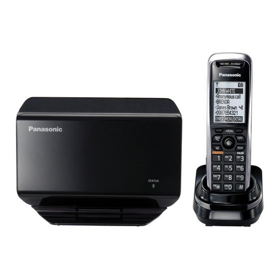
Summary of Contents for Panasonic KX-TGP500B04
- Page 1 ORDER NO. KM41003071CE Telephone Equipment KX-TGP500B04 Model No. KX-TPA50B04 SIP Cordless Phone Matte Black Version (for U.S.A.) © Panasonic System Networks Co., Ltd. 2010 Unauthorized copying and distribution is a violation of law.
- Page 2 KX-TGP500B04/KX-TPA50B04...
-
Page 3: Table Of Contents
KX-TGP500B04/KX-TPA50B04 TABLE OF CONTENTS PAGE PAGE 1 Safety Precautions----------------------------------------------- 4 14.3. Schematic Diagram (Base Unit_Main_LAN 1.1. For Service Technicians --------------------------------- 4 Block) ----------------------------------------------------- 104 2 Warning -------------------------------------------------------------- 4 14.4. Schematic Diagram (Base Unit_Main_Power) - 105 2.1. Battery Caution--------------------------------------------- 4 14.5. Schematic Diagram (Base Unit_RF Part)-------- 106 2.2. -
Page 4: Safety Precautions
KX-TGP500B04/KX-TPA50B04 1 Safety Precautions 1.1. For Service Technicians • Repair service shall be provided in accordance with repair technology information such as service manual so as to prevent fires, injury or electric shock, which can be caused by improper repair work. -
Page 5: Discarding Of P. C. Board
KX-TGP500B04/KX-TPA50B04 2.2.1. Suggested PbF Solder There are several types of PbF solder available commercially. While this product is manufactured using Tin, Silver, and Copper (Sn+Ag+Cu), you can also use Tin and Copper (Sn+Cu), or Tin, Zinc, and Bismuth (Sn+Zn+Bi). Please check the manufacturer's specific instructions for the melting points of their products and any precautions for using their product with other materials. -
Page 6: Specifications
KX-TGP500B04/KX-TPA50B04 3 Specifications VoIP Items Specifications • G.711 µ-law, G.711 A-law, G.726 (32k), G.729A, G.722 Support Codec • 10 base-T/100 base-TX Ethernet RJ-45 connector × 1 Interface VoIP Status indication • STATUS indicator on the Base Unit Supported Protocols • SIP, DNS, DHCP, HTTP (client/server), FTP, TFTP •... -
Page 7: Technical Descriptions
KX-TGP500B04/KX-TPA50B04 4 Technical Descriptions 4.1. IP PHONE Description IP PHONE IP phone is a telephone service provided by utilizing IP of the packet communication protocol used in the Internet. Communicating with other party through the IP network by sending a voice, which is transformed into the digital data and divided into Packet at IP phone. -
Page 8: Us-Dect Description
KX-TGP500B04/KX-TPA50B04 4.2. US-DECT Description The frequency range of 1.92 GHz-1.93 GHz is used. Transmitting and receiving carrier between base unit and handset is same frequency. Refer to Frequency Table (P.93). 4.2.1. TDD Frame Format (Full Slot) 4.2.2. TDD Frame Format (Long Slot) for G.722 CODEC 4.2.3. - Page 9 KX-TGP500B04/KX-TPA50B04 4.2.4. Signal Flowchart in the Radio Parts Reception A voice signal from TEL line is encoded to digital data "TXDATA" (*1) by DSP (IC504) in a base unit. Then TXDATA goes to RF PART, and it's modulated to 1.9 GHz. The RF signal is amplified and fed to a selected antenna.
-
Page 10: Explanation Of Link Data Communication
KX-TGP500B04/KX-TPA50B04 4.3. Explanation of Link Data Communication 4.3.1. Calling 4.3.2. To Terminate Communication 4.3.3. Ringing... -
Page 11: Block Diagram (Base Unit_Main)
KX-TGP500B04/KX-TPA50B04 4.4. Block Diagram (Base Unit_Main) -
Page 12: Block Diagram (Base Unit_Rf Part)
KX-TGP500B04/KX-TPA50B04 4.5. Block Diagram (Base Unit_RF Part) -
Page 13: Circuit Operation (Base Unit)
KX-TGP500B04/KX-TPA50B04 4.6. Circuit Operation (Base Unit) General Description: (DSP, Flash Memory) is a digital speech/signal processing system that implements all the functions of speech compression, and memory management. The DSP system is fully controlled by a host processor DSP. The host processor provides activation and control of all that functions as follows. - Page 14 KX-TGP500B04/KX-TPA50B04 4.6.2. Data Flash Memory (IC501) Following information data is stored. • Settings ex: message numbers, ID code, MAC address, Phone book. 4.6.3. Program Flash Memory (IC502) • IP-Phone Application program and config Data are stored. 4.6.4. Power Supply Circuit Function: The power supply voltage from AC adaptor is converted to the desired voltage of each block.
- Page 15 KX-TGP500B04/KX-TPA50B04 4.6.5. Reset Circuit Function: This circuit is used to initialize the microcomputer when it incorporates an AC adaptor. Circuit Operation: When the AC Adaptor is inserted into the unit, then the voltage is shifted by IC303 and power is supplied to the DSP.
-
Page 16: Block Diagram (Handset)
KX-TGP500B04/KX-TPA50B04 4.7. Block Diagram (Handset) IC546 ANT2 ANT1 X501 Flash 13.824 MHz Memory Q531 CHG_DET CHARGE DETECT Q362, Q364 RF part CHARGE CHG_CTL CONTROL SYN_OUT SYN_EN SYN_CLK RESET SYN_DATA Q361 SLOT_CTROL D361 CHARGE RADIO_EN IC374 TXDATA RXDATA RF_RSTN IC371 2.7 V... -
Page 17: Block Diagram (Handset_Rf Part)
KX-TGP500B04/KX-TPA50B04 4.8. Block Diagram (Handset_RF Part) -
Page 18: Circuit Operation (Handset)
KX-TGP500B04/KX-TPA50B04 4.9. Circuit Operation (Handset) 4.9.1. Construction The circuit mainly consists of DSP and RF part as shown in the block diagram. 4.9.1.1. DSP: IC501 Function • Battery Low, Power down detect circuit • Ringer Generation • Interface circuit RF part, Speaker, Mic, LED, Key scan, LCD, Headset... - Page 19 KX-TGP500B04/KX-TPA50B04 4.9.2. Power Supply Circuit Voltage is supplied separately to each block. 4.9.3. Ringer and Handset SP-Phone...
- Page 20 KX-TGP500B04/KX-TPA50B04 4.9.4. Sending Signal The voice signal from the microphone is input to DSP (90, 91). CN431 is the headset jack. When the headphone is connected, the R436/R437 detects it. The input from the microphone of the handset (MIM, MIP) is cut and the microphone signal from the headset is input to DSP (95).
-
Page 21: Circuit Operation (Rf Part)
KX-TGP500B04/KX-TPA50B04 4.10. Circuit Operation (RF Part) General Description: RF part includes Transmitter and Receiver functions. Digital signals (Mainly voice data) that come from DSP, are modulated and are transmitted. On the other hand, received signals are demodulated and go out to DSP. -
Page 22: Circuit Operation (Charger Unit)
KX-TGP500B04/KX-TPA50B04 4.11. Circuit Operation (Charger Unit) The voltage from the AC adaptor is supplied to the charge circuits. Main charge (220~280 mA at the Battery) of maximum 6- hours is started soon after the handset is placed on the charger unit. Then it changes to Trickle charge to prevent from overcharging. -
Page 23: Signal Route
KX-TGP500B04/KX-TPA50B04 4.12. Signal Route... -
Page 24: Location Of Controls And Components
KX-TGP500B04/KX-TPA50B04 5 Location of Controls and Components Refer to the Operating Instructions. Note: You can download and refer to the Operating Instructions (Instruction book) on TSN Server. 6 Installation Instructions Refer to the Operating Instructions. Note: You can download and refer to the Operating Instructions (Instruction book) on TSN Server. -
Page 25: Test Mode
KX-TGP500B04/KX-TPA50B04 8 Test Mode 8.1. Adjustment and Test Mode Flow Chart 8.1.1. Test Burst Mode for Base Unit Set up Base unit in Test mode through USB. (Refer to USB Test Mode (P.43).) Step Test Command Content Description Enter test mode Make sure the Echo back “TEST”... - Page 26 KX-TGP500B04/KX-TPA50B04 8.1.3. RX-CW Test Mode for Base Unit Set up Base unit in Test mode through USB. (Refer to USB Test Mode (P.43).) Step Test Command Content Description Enter test mode Make sure the Echo back “TEST” after this command.
- Page 27 KX-TGP500B04/KX-TPA50B04 8.1.5. Adjustment Mode for Base Unit Set up Base unit in Test mode through USB. (Refer to USB Test Mode (P.43).) Step Test Command Content Description Enter test mode Make sure the Echo back “TEST” after this command. XX: 00 - 3F (HEX) Adjust the BMC_CLK frequency Write the adjust value in XCR register.
- Page 28 KX-TGP500B04/KX-TPA50B04 8.1.6. TX-CW Mode for Handset Note: (*1) LCD displays the Channel number. (exception: default/ CH01 = 01ch.) (*2) Refer to Check Table for RF part (P.73).
- Page 29 KX-TGP500B04/KX-TPA50B04 8.1.7. RX-CW Test Mode for Handset Note: (*1) LCD displays the Channel number. (exception: default/ CH01 = 01ch.) (*2) Refer to Check Table for RF part (P.73).
- Page 30 KX-TGP500B04/KX-TPA50B04 8.1.8. Test Link Mode for Handset Note: (*1) LCD displays the Channel number. (exception: default/ CH01 = 01ch.) (*2) If can not proceed to the next step, refer to Registering a handset to the base unit in the Operating Instructions.
- Page 31 KX-TGP500B04/KX-TPA50B04 8.1.9. Adjustment Mode for Handset Cross Reference (*1) Adjust Battery Low Detector Voltage (Handset) (P.90) Note: (*2) These are the default values. (*3) These values may not be fixed depending on the battery strength.
-
Page 32: Peer To Peer Mode Test
KX-TGP500B04/KX-TPA50B04 8.2. Peer to Peer Mode Test This is for VoIP communication TEST. Setting of PC and Unit are required before communication test by Peer to Peer Mode. Refer to from Preparation (P.32) to Connection for Test (P.41). 8.2.1. Preparation Prepared device: •... - Page 33 KX-TGP500B04/KX-TPA50B04 2) Right-click the Local Area Connection icon, then select [Properties]. 3) Open the TCP/IP properties, and set each parameter as follows. • Use the following IP address. IP address: 192.168.0.1 Subnet mask: 255.255.255.0 Default gateway:... (blank) • Use the following DNS server addresses.
- Page 34 KX-TGP500B04/KX-TPA50B04 8.2.3. Web Browser Setting (Internet Explorer) 1. Start “Internet Explorer” on your PC for configuration. 2. Click [Tools] then select [Internet Options...]. 3. Click [Connections] tab, then click [LAN settings...]. 4. Confirm that “Use a proxy server for your LAN” check box isn’t checked.
- Page 35 KX-TGP500B04/KX-TPA50B04 8.2.4. How to Login to Panasonic Administrator Menu Connections: 1. Power on the unit and set the fixed IP address. 1-1. Plug the Base unit’s AC adaptor. 1-2. Insert battery in Handset. 1-3. Using phone user interface, confirm the following settings and write them down.
- Page 36 KX-TGP500B04/KX-TPA50B04 Login to Panasonic Administrator Menu: 1. Using phone user interface, set “Embedded web” to “On“ 2. Access the following address using “Internet Explorer”. http://192.168.0.241 3. Enter your user name and password into the window and click [OK] button. User name : customerserviceid...
- Page 37 Follow the same procedure as “Connections” of “How to Login to Panasonic Administrator Menu (P.35)”. Login to Panasonic Administrator Menu: Follow the same procedure as “Login to Panasonic Administrator Menu” of “How to Login to Panasonic Administrator Menu (P.35)”. Configuration: 1.
- Page 38 KX-TGP500B04/KX-TPA50B04 8.2.5.2. Set up by USB Test Mode Set up Base unit in Test mode through USB. (Refer to USB Test Mode (P.43).) Step Test Command Content Description Enter test mode Make sure the Echo back “TEST” after this command.
- Page 39 Follow the same procedure as “Connections” of “How to Login to Panasonic Administrator Menu (P.35)”. Login to Panasonic Administrator Menu: Follow the same procedure as “Login to Panasonic Administrator Menu” of “How to Login to Panasonic Administrator Menu (P.35)”. Configuration: 1.
- Page 40 KX-TGP500B04/KX-TPA50B04 8.2.6.2. Set up by USB Test Mode Set up Base unit in Test mode through USB. (Refer to USB Test Mode (P.43).) Step Test Command Content Description Enter test mode Make sure the Echo back “TEST” after this command.
- Page 41 KX-TGP500B04/KX-TPA50B04 8.2.7. Connection for Test 1. Connect LAN port on Base unit (for reference) to LAN port on base unit (for test) with Ethernet (LAN) cable. 2. Plug the each unit's (for test and reference) AC adaptor. 3. Confirm the status of each unit indicator as follows.
- Page 42 But except step 1-3 and 1-4 because the IP address is already fixed. Login to Panasonic Administrator Menu: Follow the same procedure as “Login to Panasonic Administrator Menu” of “How to Login to Panasonic Administrator Menu (P.35)”. • Access to ID ADDRESS for Test : http//192.168.0.241 •...
-
Page 43: Usb Test Mode
KX-TGP500B04/KX-TPA50B04 8.3. USB Test Mode The various tests are available by using USB communication with your PC. So all of the tests, except for the key check process, can be operated without pressing keys. Following tests are described in this service manual. - Page 44 KX-TGP500B04/KX-TPA50B04 8.3.1.2. USB Cable Connection Preparation: • USB cable : PQJA10166Z USB connection 1. Make a USB JIG cable of PQJA10166Z by removing its Refer to Fig. 1_USB JIG cable (P.44). USB plug on the PC side. 2. Open the cabinet cover.
- Page 45 KX-TGP500B04/KX-TPA50B04 8.3.1.3. PC Setting Preparation: • PC • Batch file CD-ROM for settings: PQZZGT1500M • Base Unit / Handset 1. Install the TeraTerm Install the "Teratermpro.exe" to your PC from internet site. Refer to the "readme" of the TeraTerm for installation process etc.
- Page 46 KX-TGP500B04/KX-TPA50B04 3-2.Extract the "TestModeV115.zip" to your PC. 3-3. Initialize the Test mode application. (2) Right-click on the title bar. (1) Execute "UsbSetup.exe". (3) Click the "Setting". (5) Select your PC ’ (5) Select your PC's USB. (4) Select "HCS" model.
- Page 47 KX-TGP500B04/KX-TPA50B04 4-1. Teraterm will be activated automatically if disconnect and reconnect a PC and the base unit by a USB cable. 4-2. Select "Serial port" from "Setup" menu. • Change the settings of "Serial port setup" as follows. Then click OK.
-
Page 48: Service Mode
KX-TGP500B04/KX-TPA50B04 9 Service Mode 9.1. How to Clear User Setting Units are reset to the Factory settings by this operation (Erase stored Phone numbers, Caller list and etc.). This operation should not be performed for a usual repair. 9.1.1. Base Unit Set up Base unit in Test mode through USB. -
Page 49: Handset Operation Using The Direct Commands For Ip Settings
KX-TGP500B04/KX-TPA50B04 9.2. Handset Operation Using the Direct Commands for IP Settings Item Sub-item Direct command [MENU] → [#] [5] [0] [8] 1. MAC address display [MENU] → [#] [5] [2] [6] 2. Status display (*1) [MENU] → [#] [5] [3] [0] 3. -
Page 50: Web User Interface
KX-TGP500B04/KX-TPA50B04 9.3. Web User Interface 9.3.1. Web user interface Parameter List The following tables show all the parameters of web user interface for Customer Service. Menu/Title Version Information Status Network Status VoIP Status Test Mode Settings Local Firmware Update Maintenance... - Page 51 KX-TGP500B04/KX-TPA50B04 9.3.3. Version Information 1. Click [Status] button of tab, and click [Version Information] button of menu. 2. Allows you to view current version information such as the model number and the firmware version of the unit. 9.3.4. Network Status 1.
- Page 52 KX-TGP500B04/KX-TPA50B04 9.3.5. VoIP Status 1. Click [Status] button of tab, and click [VoIP Status] button of menu. 2. Allows you to view the current VoIP status of the unit for each line. 3. Clicking [Refresh] button updates the status information displayed on the screen.
- Page 53 KX-TGP500B04/KX-TPA50B04 9.3.7. Local Firmware Update 1. Click [Maintenance] button of tab, and click [Local Firmware Update] button of menu. 2. Select the Encryption (Yes / No). 3. Click [Browse...] button and choose an update file, then click [Update Firmware] button.
- Page 54 KX-TGP500B04/KX-TPA50B04 9.3.9. Restart 1. Click [Maintenance] button of tab, and click [Restart] button of menu. 2. Allows you to restart the base unit by clicking [Restart]. After clicking this button, a dialog box is displayed to ask you whether to restart the base unit. Click [OK] to perform a restart, or [Cancel] not to.
-
Page 55: Ip Reset
KX-TGP500B04/KX-TPA50B04 9.4. IP Reset... -
Page 56: How To Change Mac Address Label (Procedure After Replacing The Main P.c.board Of Base Unit)
KX-TGP500B04/KX-TPA50B04 9.5. How to Change MAC Address Label (Procedure after Replacing the Main P.C.Board of Base Unit) When replacing the Main P.C.Board on the Base Unit, customer data shall be renewed before sticking the included MAC/Serial label. 9.5.1. Replacing Main P.C.Board Note: (*1) : If you reuse defective P.C.Board for another repairing unit by repairing. - Page 57 KX-TGP500B04/KX-TPA50B04 9.5.2. Attaching MAC Address and Serial Number Label Attach the new MAC address label and new Serial number label to the base unit by placing over the old label.
-
Page 58: Troubleshooting Guide
KX-TGP500B04/KX-TPA50B04 10 Troubleshooting Guide 10.1. Troubleshooting Flowchart Cross Reference: Check Power (P.59) Check Status Indicator (P.60) Peer to Peer Mode Test (P.32) Check Battery Charge (P.70) Check CDL Link (P.61) Check the RF part (P.71) Check Handset Transmission (P.79) Check Handset Reception (P.79) - Page 59 KX-TGP500B04/KX-TPA50B04 10.1.1. Check Power Cross Reference: Note: Power Supply Circuit (P.14) DSP is IC504. Reset Circuit (P.15) (*1) Refer to Specifications (P.6) for part number and supply voltage of AC adaptor. (*2) Refer to Circuit Board (Base Unit_Main) (P.113).
- Page 60 KX-TGP500B04/KX-TPA50B04 10.1.2. Check Status Indicator Cross Reference: Failure Analysis of DSP, FLASH ROM and RAM (Base Unit) (P.80) IP Troubleshooting (P.62)
- Page 61 KX-TGP500B04/KX-TPA50B04 10.1.3. Check CDL Link Note: (*1) Refer to Finding out the Defective part (P.71) Cross Reference: Check the RF part (P.71)
- Page 62 KX-TGP500B04/KX-TPA50B04 10.1.4. IP Troubleshooting 10.1.4.1. IP Troubleshooting Simplified Chart VoIP - Status display Display the access status of the IP network. • Enter [MENU] → [#]→ [5]→[2]→[6] to display current IP network access condition as 4 integers (status code) and each line condition as 8 integers (status code).
- Page 63 KX-TGP500B04/KX-TPA50B04 10.1.4.2. IP Check Note: (*1) If the router has a single LAN port only, add ports as needed by using hubs. (*2) Refer to Setting Up for Test Unit (P.39) for “Test mode”. (*3) Refer to Peer to Peer Mode Test (P.32).
- Page 64 KX-TGP500B04/KX-TPA50B04 10.1.4.3. Hub Check This flow chart is designed for a single hub connection form (*1). If multiple hubs are connected (*2), be careful with the followings. • An error may occurs if more than 5 repeater hubs are connected with cascading connection (*3) •...
- Page 65 KX-TGP500B04/KX-TPA50B04 10.1.4.3.1. Switching Hub Check...
- Page 66 KX-TGP500B04/KX-TPA50B04 10.1.4.3.2. Repeater Hub Check...
- Page 67 KX-TGP500B04/KX-TPA50B04 10.1.4.4. Router Check...
- Page 68 KX-TGP500B04/KX-TPA50B04 10.1.4.5. Modem Check...
- Page 69 KX-TGP500B04/KX-TPA50B04 10.1.4.6. IP Duplication Check...
- Page 70 KX-TGP500B04/KX-TPA50B04 10.1.5. Check Battery Charge Note: (*1) Refer to Specifications (P.6) for part number and supply voltage of AC adaptor.
- Page 71 KX-TGP500B04/KX-TPA50B04 10.1.6. Check the RF part 10.1.6.1. Finding out the Defective part After All the Checkings or Repairing 1. Re-register the checked handset to the checked base unit, and Regular HS to Regular BU. Note: (*1) HS: Handset (*2) BU: Base Unit...
- Page 72 KX-TGP500B04/KX-TPA50B04 10.1.6.2. RF Check Flowchart Each item (1 ~ 6) of RF Check Flowchart corresponds to Check Table for RF part (P.73). Please refer to the each item. Note: (*1) Refer to Things to Do after Replacing IC (P.90).
- Page 73 KX-TGP500B04/KX-TPA50B04 10.1.6.3. Check Table for RF part For Normal Link, need Peer to Peer Mode Test (P.32). Item BU (Base Unit) Check HS (Handset) Check Link Confirmation Normal 1. Register Regular HS to BU (to be 1. Register HS (to be checked) to Regular checked).
- Page 74 KX-TGP500B04/KX-TPA50B04 10.1.6.4. TEST RANGE Check Circuit block which range is defective can be found by the following check. Under Test mode Link, No voice conversation is enabled.(*2) Item BU (Base Unit) Check HS (Handset) Check Range Confirmation TX TEST 1. Register Regular HS to BU (to be checked).
- Page 75 KX-TGP500B04/KX-TPA50B04 10.1.6.5. RF-DSP Interface Signal Wave Form FP (Base)
- Page 76 KX-TGP500B04/KX-TPA50B04 PP (Handset)
- Page 77 KX-TGP500B04/KX-TPA50B04...
- Page 78 KX-TGP500B04/KX-TPA50B04...
- Page 79 KX-TGP500B04/KX-TPA50B04 10.1.7. Check Handset Transmission Cross Reference: Signal Route (P.23) 10.1.8. Check Handset Reception Cross Reference: Signal Route (P.23) Note: When checking the RF part, Refer to Check the RF part (P.71).
-
Page 80: Failure Analysis Of Dsp, Flash Rom And Ram (Base Unit)
KX-TGP500B04/KX-TPA50B04 10.2. Failure Analysis of DSP, FLASH ROM and RAM (Base Unit) It is difficult to find the defective parts causing operation failure in this unit because DSP, FLASH ROM and RAM are connected to the same bus line. This unit has two ports as the means to watch the operation of DSP, FLASH ROM, RAM, etc. during the start-up process. The following conditions can be confirmed with these two ports. - Page 81 KX-TGP500B04/KX-TPA50B04...
- Page 82 KX-TGP500B04/KX-TPA50B04 Parts1 3.3 V, VCC, X501, R575, IC505, C558,R638, C550, R322 R323, R321, C331, R320, Q305, Q304, R317 Parts2 3.3_MEM, IC502, R538, R540, C506, C508,C513, R572, R507 R508, R581, R509, R511, R501, R624, R503, R510, R512 R502, R505, R517, R504, R506, R514, R515, R592, R518...
- Page 83 KX-TGP500B04/KX-TPA50B04 NG Examples Program Flash (IC503) NG Wave RAM (IC505) NG Wave...
- Page 84 KX-TGP500B04/KX-TPA50B04 Data Flash (IC502) NG Wave...
-
Page 85: Disassembly And Assembly Instructions
KX-TGP500B04/KX-TPA50B04 11 Disassembly and Assembly Instructions 11.1. Disassembly Instructions 11.1.1. Base Unit... - Page 86 KX-TGP500B04/KX-TPA50B04 11.1.2. Handset...
- Page 87 KX-TGP500B04/KX-TPA50B04 11.1.3. Charger Unit...
-
Page 88: How To Replace The Handset Lcd
KX-TGP500B04/KX-TPA50B04 11.2. How to Replace the Handset LCD... - Page 89 KX-TGP500B04/KX-TPA50B04...
-
Page 90: Measurements And Adjustments
KX-TGP500B04/KX-TPA50B04 12 Measurements and Adjustments 12.1. Things to Do after Replacing IC 12.1.1. X501 (Base Unit), X501 (Handset) Check Equipment: Frequency counter Check Point for measurement: BCK Checking tolerance: 13.824 MHz ± 50 Hz (Base Unit) / 13.824 MHz ± 50 Hz (Handset) 12.1.1.1. -
Page 91: Base Unit Reference Drawing
KX-TGP500B04/KX-TPA50B04 12.2. Base Unit Reference Drawing When connecting the simulator equipment for checking, please refer to below. C572 R550 C534 C571 C518 C528 R551 C519 C532 R552 C522 R553 C535 C524 R554 C526 C537 R555 C529 C520 R556 C523 C533... -
Page 92: Handset Reference Drawing
KX-TGP500B04/KX-TPA50B04 12.3. Handset Reference Drawing When connecting the simulator equipment for checking, please refer to below. D423 D424 PNLB1127Z KX-TPA50 PNLPTPA50 C577 PNLPTGA740 KX-TGA740 ANT1 C566 R578 C575 C578 R580 ANT2 C562 IC561 C568 R560 C564 Q561 ANT1 C567 C792... -
Page 93: Frequency Table
KX-TGP500B04/KX-TPA50B04 12.4. Frequency Table Ch.(hex) TX/RX Frequency (MHz) Channel 0 1928.448 Channel 1 1926.720 Channel 2 1924.992 Channel 3 1923.264 Channel 4 1921.536... -
Page 94: Miscellaneous
KX-TGP500B04/KX-TPA50B04 13 Miscellaneous 13.1. Explanation of IC Terminals (RF Part) IC701 13.1.1. -
Page 95: How To Replace The Flat Package Ic
KX-TGP500B04/KX-TPA50B04 13.2. How to Replace the Flat Package IC 13.2.1. Preparation • PbF (: Pb free) Solder • Soldering Iron Tip Temperature of 700°F ± 20°F (370°C ± 10°C) Note: We recommend a 30 to 40 Watt soldering iron. An expert may be able to use a 60 to 80 Watt iron where someone with less experience could overheat and damage the PCB foil. - Page 96 KX-TGP500B04/KX-TPA50B04 13.2.3. How to Install the IC 1. Temporarily fix the FLAT PACKAGE IC, soldering the two marked pins. *Check the accuracy of the IC setting with the corresponding soldering foil. 2. Apply flux to all pins of the FLAT PACKAGE IC.
-
Page 97: How To Replace The Shield Case
KX-TGP500B04/KX-TPA50B04 13.3. How to Replace the Shield Case 13.3.1. Preparation • PbF (: Pb free) Solder • Soldering Iron Tip Temperature of 700°F ± 20°F (370°C ± 10°C) Note: We recommend a 30 to 40 Watt soldering iron. An expert may be able to use a 60 to 80 Watt iron where someone with less experience could overheat and damage the PCB foil. - Page 98 KX-TGP500B04/KX-TPA50B04 13.3.3. How to Install the Shield Case Note: • If you don’t have special tools (ex. Hot air disordering tool), conduct the following operations. • Shield case’s No. : PNMC1014Z 1. Put the shield case. 2. Solder the surroundings.
- Page 99 KX-TGP500B04/KX-TPA50B04 13.3.5. How to Install the IC 1. Place the solder a little on the land where the radiation GND pad on IC bottom is to be attached. 2. Place the solder a little on the land where IC pins are to be attached, then place the IC.
-
Page 100: Terminal Guide Of The Ics, Transistors And Diodes
KX-TGP500B04/KX-TPA50B04 13.4. Terminal Guide of the ICs, Transistors and Diodes 13.4.1. Base Unit 13.4.2. Handset... -
Page 101: Schematic Diagram
KX-TGP500B04/KX-TPA50B04 14 Schematic Diagram 14.1. For Schematic Diagram 14.1.1. Base Unit (Schematic Diagram (Base Unit_Main)) Notes: 1. DC voltage measurements are taken with voltmeter from the negative voltage line. 2. The schematic diagrams may be modified at any time with the development of new technology. -
Page 102: Block)
KX-TGP500B04/KX-TPA50B04 14.2. Schematic Diagram (Base Unit_Main_DSP Block) C534 R550 DW_BCLK BCLK BCLK SYN_OUT R551 33 SYN_OUT RF_SYN_OUT SYN_EN R552 33 SYN_EN RF_SYN_EN SYN_CLK R553 33 SYN_CLK RF_SYN_CLK SYN_DATA R554 33 SYN_DATA RF_SYN_DATA SLOT_CTRL R555 33 SLOT_CTRL RF_SLOT_CTRL RADIO_EN R556 33... - Page 103 KX-TGP500B04/KX-TPA50B04 3.3V_MEM 3.3V C560 100n C561 100n C562 100n C563 100n C564 100n C565 100n C566 100n C567 100n C568 100n C569 100n C570 100n C571 100n C572 100n C530 C573 100n C574 100n CL582 CL581 C575 100n C531 C576 100n...
-
Page 104: Block)
KX-TGP500B04/KX-TPA50B04 14.3. Schematic Diagram (Base Unit_Main_LAN Block) 3.3V_PHY R423 R407 6.49k C415 100n C406 C407 DG DG R422 1_TX+ 4_TXT R402 5_TXT 2_TX- E_RXDV 3_RX+ E_RXCLK 7_RXT E_RX_ER 8_RXT IC401 R401 R405 4.7k 6_RX- *INT E_TXCLK L401 GND2 VDDA_3.3 E_TXEN L402 VDDPLL_1.8... -
Page 105: Schematic Diagram (Base Unit_Main_Power)
KX-TGP500B04/KX-TPA50B04 14.4. Schematic Diagram (Base Unit_Main_Power) -
Page 106: Schematic Diagram (Base Unit_Rf Part)
KX-TGP500B04/KX-TPA50B04 14.5. Schematic Diagram (Base Unit_RF Part) C793 D10p L791 2.7n ANT2 D771 C776 B1.5p C773 D781 1.5p C797 L795 1.8n D10p ANT1 C765 C763 1.5p NC: No Components... - Page 107 KX-TGP500B04/KX-TPA50B04 PP:3.1V V_RF FP:3.3V C721 J100p BCLK RF_SYN_OUT RA731 RF_SYN_EN RF_SYN_CLK RF_SYN_DATA VCC_VCO SYN_CLK RF_SLOT_CTRL PAEN SYN_DAT R731 ATSTp W0.2 X L8.0mm W0.2 X L8.0mm ATST_p SLOT_CTRL RF_RADIO_EN ATST_n RADIOEN PGND ANT_n TR_DATA TRSW VCC_IO RSTN VCC_DIG IC701 R736 NC...
-
Page 108: Schematic Diagram (Handset_Main)
KX-TGP500B04/KX-TPA50B04 14.6. Schematic Diagram (Handset_Main) RF circuit TXO BCLK R540 BCLK C540 K0.1 TX_DATA TX_DATA SLOT_CTRL SLOT_CTRL RX_DATA RX_DATA DVCC RADIO_EN RF control line RF_RSTN RF_RSTN 2.7V SYN_DATA X501 SYN_DATA C547 100u NC C519 C515 SYN_EN 13.824MHz SYN_EN K0.1 R501... - Page 109 KX-TGP500B04/KX-TPA50B04 Test Signal:1kHz SP phone RX Input from Dummy Set PP MIC: -45dBm/600 (MIC M ute : O N) 2.85V p - p /8 (V ol .M ax ) Voice circuit SP_PHONE 2.7V GND_0 GND_0 R436 R431 C439 J330p CN431...
-
Page 110: Schematic Diagram (Handset_Rf Part)
KX-TGP500B04/KX-TPA50B04 14.7. Schematic Diagram (Handset_RF Part) C793 D10p L791 2.7n ANT2 C776 B1.5p C773 1.5p D781 D771 C797 D10p L795 1.8n ANT1 C763 2.2p C765 B1.0p NC: No Components... - Page 111 KX-TGP500B04/KX-TPA50B04 V_RF PP:3.1V FP:3.3V C721 J100p BCLK SYN_OUT RA731 SYN_EN SYN_CLK SYN_DATA 1 VCC_VCO SLOT_CTRL SYN_CLK 2 PAEN SYN_DAT R731 3 ATST_p W0.2 X L8.0mm W0.2 X L8.0mm ATSTp RADIO_EN SLOT_CTRL 4 ATST_n RADIOEN PGND 5 ANT_n TR_DATA 6 TRSW...
-
Page 112: Schematic Diagram (Charger Unit)
KX-TGP500B04/KX-TPA50B04 14.8. Schematic Diagram (Charger Unit) 12 (2W) NC: No Components SCHEMATIC DIAGRAM (Charger Unit) -
Page 113: Printed Circuit Board
KX-TGP500B04/KX-TPA50B04 15 Printed Circuit Board 15.1. Circuit Board (Base Unit_Main) 15.1.1. Component View SW503 D501 D502 R654 R655 C585 SYN_OUT SYN_EN C792 R782 SYN_CLK DTEST1 DTEST L791 SYN_DATA C795 ATSTp SLOT_CTRL R731 RADIO_EN C775 R736 TR_DATA R772 C715 D771 L739... - Page 114 KX-TGP500B04/KX-TPA50B04 15.1.2. Bottom View XOUT (BCLK) C572 R550 C534 C571 C518 C528 R551 C519 C532 R552 C522 R553 C535 C524 R554 C526 C537 R555 C520 C529 R556 C523 C533 C536 C525 R557 C570 C538 C527 R784 R558 R666 USB_GND USB_V+...
-
Page 115: Circuit Board (Base Unit_Rf Part)
KX-TGP500B04/KX-TPA50B04 15.2. Circuit Board (Base Unit_RF Part) SHIELD L796 C754 C702 C762 C752 C701 C765 C737 C763 C757 C708 C710 R771 C771 C707 C703 C751 R715 C758 L739 D771 C715 R772 R736 C775 R731 ATSTp C795 L791 DTEST DTEST1 R782... - Page 116 KX-TGP500B04/KX-TPA50B04 Note...
-
Page 117: Circuit Board (Handset_Main)
KX-TGP500B04/KX-TPA50B04 15.3. Circuit Board (Handset_Main) 15.3.1. Component View D423 D420 D421 D424 PNLB1127Z KX-TPA50 PNLPTPA50 C577 PNLPTGA740 KX-TGA740 ANT1 C566 R578 C575 C578 R580 ANT2 V_BACK LIGHT C562 (5.0V) IC561 C568 R560 C564 Q561 D429 D428 ANT1 C567 C792 R782... - Page 118 KX-TGP500B04/KX-TPA50B04 15.3.2. Bottom View LEFT RIGHT TALK LED559 LED558 FLASH KX-TPA50 CIRCUIT BOARD (Handset_Main (Bottom View))
-
Page 119: Circuit Board (Handset_Rf Part)
KX-TGP500B04/KX-TPA50B04 15.4. Circuit Board (Handset_RF Part) C792 R782 L791 DTEST1 DTEST C795 R731 C775 R736 R772 C715 L739 D771 C758 R715 C751 C703 C707 C771 R771 C710 C708 C765 C757 C763 C737 C754 C701 C752 C762 C702 L796 SHIELD KX-TPA50 CIRCUIT BOARD (Handset_RF (Component View)) -
Page 120: Circuit Board (Charger Unit)
KX-TGP500B04/KX-TPA50B04 15.5. Circuit Board (Charger Unit) 15.5.1. Component View CIRCUIT BOARD (Charger unit (Component View)) 15.5.2. Bottom View TP4 (GND) CIRCUIT BOARD (Charger unit (Bottom View)) -
Page 121: Exploded View And Replacement Parts List
KX-TGP500B04/KX-TPA50B04 16 Exploded View and Replacement Parts List 16.1. Cabinet and Electrical Parts (Base Unit) PCB1 6 (*1) Ref.No. Figure Note: (*1) Cut the LED LENS in half as shown in the illustration above. -
Page 122: Cabinet And Electrical Parts (Handset)
(*1) This cable is fixed by welding. Refer to How to Replace the Handset LCD (P.88). (*2) Refer to Handset (P.100) of Terminal Guide of the ICs, Transistors and Diodes. (*3) The rechargeable Ni-MH battery (HHR-4DPA) is available through sales route of Panasonic. (*4) Attach the SPACER (No. 121) to the exact location described above. -
Page 123: Cabinet And Electrical Parts (Charger Unit)
KX-TGP500B04/KX-TPA50B04 16.3. Cabinet and Electrical Parts (Charger Unit) 200-1 PCB200 200-2 200-3 200-4 Ref.No. Figure... -
Page 124: Accessories And Packing Materials
KX-TGP500B04/KX-TPA50B04 16.4. Accessories and Packing Materials 16.4.1. KX-TGP500B04... - Page 125 KX-TGP500B04/KX-TPA50B04 16.4.2. KX-TPA50B04 (*1) A101 A103 A102 P101 Note: (*1) These pads are pieces of Ref No. P101 (GIFT BOX).
-
Page 126: Replacement Parts List
KX-TGP500B04/KX-TPA50B04 16.5. Replacement Parts List 16.5.1.2. Main P.C. Board Parts Note: Note: (*1) When replacing Main P. C. Board Ass’y (PCB1), refer to 1. RTL (Retention Time Limited) How to Change MAC Address Label (Procedure after The marking (RTL) indicates that the Retention Time is Replacing the Main P.C.Board of Base Unit) (P.56). - Page 127 KX-TGP500B04/KX-TPA50B04 Safety Ref. Part No. Part Name & Description Remarks Safety Ref. Part No. Part Name & Description Remarks X401 H0J250500086 CRYSTAL OSCILLATOR R585 ERJ2GEJ331 X501 H0J138500011 CRYSTAL OSCILLATOR (*2) R586 ERJ2GEJ101 (RESISTORS) R590 ERJ2GEJ470 L796 ERJ2GE0R00 R592 ERJ2GEJ101 R303...
- Page 128 KX-TGP500B04/KX-TPA50B04 Safety Ref. Part No. Part Name & Description Remarks Safety Ref. Part No. Part Name & Description Remarks C409 ECUE0J105KBQ 1 C711 ECUE1H100DCQ 10p C410 ECUE1A104KBQ 0.1 C712 ECUE1A104KBQ 0.1 C411 ECUE1A104KBQ 0.1 C714 ECUE0J105KBQ 1 C415 ECUE1A104KBQ 0.1 C715 ECUE1A104KBQ 0.1...
- Page 129 KX-TGP500B04/KX-TPA50B04 16.5.2.2. Main P.C. Board Parts Safety Ref. Part No. Part Name & Description Remarks Note: RA501 D1H84724A013 RESISTOR ARRAY (*1) When you have replaced IC501 or IC546, adjust X501. RA551 D1H84714A013 RESISTOR ARRAY Refer to Check and Adjust X501 (Handset) Frequency...
- Page 130 ECUE1H470JCQ 47p (*1) You can download and refer to the Operating C745 F1G1H2R7A562 2.7p Instructions (Instruction book) on TSN Server. C751 ECUE1H1R5BCQ 1.5 C752 ECUE1H100DCQ 10p 16.5.4.1. KX-TGP500B04 C754 ECUE1A104KBQ 0.1 C755 ECUE1H1R5BCQ 1.5 C756 ECUE1HR50BCQ 0.5 Safety Ref. Part No.
- Page 131 KX-TGP500B04/KX-TPA50B04 16.5.4.2. KX-TPA50B04 Safety Ref. Part No. Part Name & Description Remarks A101 PQLV219Z AC ADAPTOR A102 PNQX2117Y INSTRUCTION BOOK (*1) A103 PNKE1029Z1 HANGER, BELT CLIP ABS-HB P101 PNPK2409Z GIFT BOX 16.5.5. Screws Safety Ref. Part No. Part Name & Description...
Need help?
Do you have a question about the KX-TGP500B04 and is the answer not in the manual?
Questions and answers