Table of Contents
Advertisement
Quick Links
Step-Down DC/DC Voltage Mode Controller
FEATURES
2
PMBus/I
C Compliant Serial Interface
n
– Monitor Voltage, Current, Temperature and Faults
– Program Voltage, Soft-Start/Stop, Sequencing,
Margining, AVP and UV/OV/OC Limits
3V ≤ VINSNS ≤ 38V, 0.5V ≤ V
n
±0.5% Output Voltage Error
n
Programmable PWM Frequency or External Clock
n
Synchronization from 250kHz to 1.25MHz
Accurate PolyPhase
®
n
Internal EEPROM with Fault Logging and ECC
n
IC Supply Range: 3V to 13.2V
n
Resistor or Inductor DCR Current Sensing
n
Power Good Output Voltage Monitor
n
Optional Resistor Programming for Key Parameters
n
40-Pin (6mm × 6mm) QFN Package
n
APPLICATIONS
High Current Distributed Power Systems
n
Servers, Network and Storage Equipment
n
Intelligent Energy Efficient Power Regulation
n
TYPICAL APPLICATION
V
IN
7V TO 13.2V
V
VINSNS
CC
V
LTC3882-1
SDA
SCL
TO/FROM
ALERT
MCU
RUN0
RUN1
PGOOD0
I
FAULT0
I
TO/FROM
PGOOD1
V
EXTERNAL DEVICES
FAULT1
I
SYNC
I
SHARE_CLK
I
AVG0
I
AVG1
I
AVG_GND
V
V
GND
Document Feedback
with Digital Power System Management
≤ 5.25V
OUT
Current Sharing
+
SENSE0
FB0
FDMF5820DC
PWM
COMP0
COMP1
PWM0
TSNS0
+
SENSE0
–
SENSE0
+
SENSE1
–
SENSE1
+
FDMF5820DC
SENSE1
PWM
PWM1
TSNS1
–
SENSE0
–
SENSE1
INDUCTORS: COOPER FP1007R1-R22
SOME DETAILS OMITTED FOR CLARITY
For more information
Dual Output PolyPhase
DESCRIPTION
The
LTC
3882-1
is a dual, PolyPhase DC/DC synchronous
®
step-down switching regulator controller with
compliant serial
interface. It uses a constant frequency,
leading-edge modulation, voltage mode architecture for
excellent transient response and output regulation. Each
PWM channel can produce output voltages from 0.5V to
5.25V using a wide range of 3.3V compatible power stages,
including power blocks, DrMOS or discrete FET drivers.
Up to four LTC3882-1 devices can operate in parallel for
2-, 3-, 4-, 6- or 8-phase operation.
System configuration and monitoring is supported by the
LTpowerPlay™
software tool. The LTC3882-1 serial interface
can read back input voltage, output voltage and current,
temperature and fault status. Most operating parameters can
be set via the digital interface or stored in internal EEPROM
for use at power up. Switching frequency and phase, output
voltage and device address can also be set using external
configuration resistors.
All registered trademarks and trademarks are the property of their respective owners. Protected
by U.S. Patents, including 5396245, 5859606, 6144194, 6937178, 7420359 and 7000125.
PWM ENABLE
OUTPUT
CONTROL
LTC3882
•
LTC3882-1
V
IN
V
SW
OUT
1V
70A
GND
10A/DIV
V
IN
SW
10A/DIV
GND
38821 TA01a
www.analog.com
LTC3882-1
TG/BG
HW WRITE
DEDICATED
PROTECT
PGOOD OUTPUT
•
•
•
Load Step Transient Current Sharing
(Using FDMF5820DC DrMOS)
I
OUT
I
, I
L0
L1
50µs/DIV
PMBus
DIFFERENTIAL
V
SENSE
OUT
V
Only
OUT0
V
& V
OUT0
OUT1
38821 TA01b
Rev A
1
Advertisement
Table of Contents

Subscribe to Our Youtube Channel
Related Manuals for Linear Technology Analog Devices LTC3882-1


Summary of Contents for Linear Technology Analog Devices LTC3882-1
-
Page 1: Features
LTC3882-1 Dual Output PolyPhase Step-Down DC/DC Voltage Mode Controller with Digital Power System Management FEATURES DESCRIPTION PMBus/I C Compliant Serial Interface 3882-1 is a dual, PolyPhase DC/DC synchronous ® – Monitor Voltage, Current, Temperature and Faults step-down switching regulator controller with PMBus –... -
Page 2: Table Of Contents
LTC3882-1 TABLE OF CONTENTS Features ............. 1 PMBus Command Summary ......37 Applications ..........1 PMBus Commands ..........37 Typical Application ........1 Data Formats ............37 Description..........1 Applications Information ........ 42 Absolute Maximum Ratings ......4 Efficiency Considerations ........42 Order Information .......... - Page 3 LTC3882-1 TABLE OF CONTENTS MFR_PWM_CONFIG_LTC3882-1 ....... 75 MFR_INFO ............90 MFR_CHAN_CONFIG_LTC3882-1 ...... 76 CLEAR_FAULTS..........90 MFR_PWM_MODE_LTC3882-1 ......77 Telemetry ..............91 Input Voltage and Limits ......... 78 READ_VIN ............91 VIN_ON .............. 78 MFR_VIN_PEAK ..........91 VIN_OFF ............. 78 READ_VOUT ............91 VIN_OV_FAULT_LIMIT ........78 MFR_VOUT_PEAK ..........
-
Page 4: Absolute Maximum Ratings
LTC3882-1 ABSOLUTE MAXIMUM RATINGS PIN CONFIGURATION (Note 1) TOP VIEW Supply Voltage ........–0.3V to 15V VINSNS Voltage ......... –0.3V to 40V – ............–0.3V to 1V SENSEn – ......–0.3V to 6V 38 37 36 35 34 33 32 31 SENSEn SENSEn SENSEn... -
Page 5: Electrical Characteristics
LTC3882-1 ELECTRICAL CHARACTERISTICS denotes the specifications which apply over the specified operating – junction temperature range, otherwise specifications are at T = 25°C (Note 2). V = 5V, V = 1.8V, V SENSE0 SENSE1 SENSE0 – = GND = 0V, f = 500kHz (externally driven) unless otherwise specified. - Page 6 LTC3882-1 ELECTRICAL CHARACTERISTICS denotes the specifications which apply over the specified operating – junction temperature range, otherwise specifications are at T = 25°C (Note 2). V = 5V, V = 1.8V, V SENSE0 SENSE1 SENSE0 – = GND = 0V, f = 500kHz (externally driven) unless otherwise specified.
- Page 7 LTC3882-1 ELECTRICAL CHARACTERISTICS denotes the specifications which apply over the specified operating – junction temperature range, otherwise specifications are at T = 25°C (Note 2). V = 5V, V = 1.8V, V SENSE0 SENSE1 SENSE0 – = GND = 0V, f = 500kHz (externally driven) unless otherwise specified.
- Page 8 LTC3882-1 ELECTRICAL CHARACTERISTICS Note 1: Stresses beyond those listed under Absolute Maximum Ratings Note 5: All currents into device pins are positive; all currents out of device may cause permanent damage to the device. Exposure to any Absolute pins are negative. All voltages are referenced to GND unless otherwise Maximum Rating condition for extended periods may affect device specified.
-
Page 9: Typical Performance Characteristics
LTC3882-1 TYPICAL PERFORMANCE CHARACTERISTICS LTC3882-1 1.0V Regulated Output Typical LTC3882-1 Output Voltage Typical LTC3882-1 Output Voltage vs Temperature Distribution at 0°C Distribution at 105°C 1.001 1000 1200 = 12V 1094 UNITS 1078 UNITS VOUT_COMMAND = 1.0V VOUT_COMMAND = 1.0V VOUT_COMMAND = 1.0V DIGITAL SERVO ENGAGED DIGITAL SERVO DIGITAL SERVO... - Page 10 LTC3882-1 TYPICAL PERFORMANCE CHARACTERISTICS 3-Phase DC Output Current Load Step Transient Current Load Dump Transient Current Sharing (Using D12S1R845A Sharing (Using FDMF6707B Sharing (Using FDMF6707B Power Block DrMOS) DrMOS) CHANNEL 1 CHANNEL 2 CHANNEL 3 20A/DIV 20A/DIV 20mV/DIV 20mV/DIV 10A/DIV 10A/DIV 38821 G10 38821 G11...
- Page 11 LTC3882-1 TYPICAL PERFORMANCE CHARACTERISTICS Soft-Start Ramp Start-Up Into a Prebiased Load Soft-Off Ramp 2V/DIV 0.5V/DIV 0.5V/DIV 1V/DIV 10A/DIV 10A/DIV 38821 G20 = 12V 1ms/DIV 38821 G18 = 12V 1ms/DIV 38821 G19 5ms/DIV TOFF_DELAY = 10ms TOFF_FALL = 5ms Regulated Output vs Temperature VOUT_COMMAND INL VOUT_COMMAND DNL 1.8000...
- Page 12 LTC3882-1 TYPICAL PERFORMANCE CHARACTERISTICS ADC TUE ADC TUE ADC TUE IN(SNS) 0.40 –1 0.30 –2 0.20 –3 0.10 –4 –5 –0.10 –2 –6 –0.20 –4 –7 –0.30 –6 –8 –0.40 –9 –8 VINSNS (V) OUTPUT CURRENT (A) 38821 G24 38821 G25 38821 G26 SHARE_CLK Frequency vs IC Operating Current vs...
-
Page 13: Pin Functions
LTC3882-1 PIN FUNCTIONS frequency with a 125ns pulse width. A pull-up resistor to COMP0/COMP1 (Pin 1/Pin 28): Error Amplifier Outputs. 3.3V is required in the application if SYNC is driven by PWM duty cycle increases with this control voltage. These any LTC3882-1. - Page 14 LTC3882-1 PIN FUNCTIONS PHAS_CFG (Pin 21): Phase Configuration Pin. Connect (Pin 36/Pin 33): Positive Output Voltage SENSE0 SENSE1 an optional 1% resistor divider between V and GND Sense Inputs. These pins must still be properly connected DD25 to this pin to configure the phase of each PWM channel on slave channels for accurate output current telemetry.
-
Page 15: Block Diagram
LTC3882-1 BLOCK DIAGRAM EEPROM VINSNS R_CONFIG AVG0 MCU AND SHARE_CLK CUSTOM ± SENSE0 LOGIC PMBus 2.5V 12-BIT PWM0 REGULATOR ± SENSE0 PGOOD0 SYNC PWM0 VOLTAGE REFERENCE AVG_GND 3.3V REGULATOR PWM1 DD33 PGOOD1 ± BIAS AND SENSE1 12-BIT PWM1 HOUSEKEEPING ± SENSE1 VINSNS PWM0... -
Page 16: Test Circuit
LTC3882-1 TEST CIRCUIT (Channel 0 Example) LTC3882-1 1.024V 12-BIT DIGITAL – – COMP0 SENSE0 SENSE0 LTC1055 TARGET = VOUT_COMMAND 38821 TC TIMING DIAGRAM SU(DAT) HD(SDA) HD(STA) SU(STA) SU(STO) HD(DAT) HIGH 38821 TD START REPEATED START STOP START CONDITION CONDITION CONDITION CONDITION OPERATION Overview... -
Page 17: Main Control Loop
LTC3882-1 OPERATION • Operating Condition Telemetry Main Control Loop • Phase Locked Loop for Synchronous PolyPhase Opera- The LTC3882-1 utilizes constant frequency voltage mode tion (2, 3, 4, 6, or 8 phases) control with leading-edge modulation. This provides improved response to a load step increase, especially at •... - Page 18 LTC3882-1 OPERATION MODE LTC3882-1 OSCILLATOR CLOCK PWM0 GATE LOGIC DRIVER 8-BIT DAC IOUT_OC_FAULT_LIMIT RAMP VINSNS FEED FORWARD SENSE0 – SENSE0 AVG0 SLAVE ENABLE AVG_GND SLAVE DETECT MASTER ENABLE 9-BIT DAC VOUT_OV_FAULT_LIMIT 9-BIT DAC VOUT_UV_FAULT_LIMIT SENSE0 (RANGE 0) LOOP COMPENSATION NETWORK 12-BIT DAC VOUT_COMMAND –...
-
Page 19: Power-Up And Initialization
LTC3882-1 OPERATION VC discriminates its positive input against an internally The LTC3882-1 features an internal RAM built-in self-test generated PWM voltage ramp. The positive input is a com- (BIST) that runs during initialization. Should RAM BIST posite control based on COMP voltage with line feedforward fail, the following steps are taken. -
Page 20: Soft-Start
LTC3882-1 OPERATION Soft-Start times. However, with LTC3882-1 digital control, on and off ramping methods need not be the same, and ramping The RUN pins are released for external control after the configurations can be reprogrammed as needed without part initializes and VINSNS is greater than the VIN_ON hardware modification. -
Page 21: Minimum Output Disable Times
LTC3882-1 OPERATION Finally, each PWM channel can be commanded off by tor current reaches approximately 0A, preventing it from pulling the associated RUN pin low. Pulling the RUN pin going substantially negative. The external gate driver or low can force the channel to perform a controlled turn off power block must have short delays to a high impedance or immediately disable the power stage, depending on the output, relative to the PWM cycle, to support DCM. -
Page 22: Polyphase Load Sharing
LTC3882-1 OPERATION can also be set from EEPROM or external configuration proportionally summed with the master error amplifier resistors as outlined in Table 10. Phase designates the COMP output to adjust the duty cycle and balance the relationship between the falling edge of SYNC and the current contribution of that phase. -
Page 23: External And Internal Temperature Sense
LTC3882-1 OPERATION of the LTC3882-1 monitor ADC, they have an input range ASEL1, V , FREQ_CFG, and PHAS_CFG. OUT0_CFG OUT1_CFG of approximately ±128mV and a noise floor of 7μV If any of these pins are left open the value stored in the Peak-peak noise is approximately 46.5μV. -
Page 24: Internal Eeprom With Crc And Ecc
LTC3882-1 OPERATION The PHAS_CFG pin settings are described in Table 10. Fault Detection This pin selects the phase relationships between the two A variety of fault and warning detection, reporting and channels and the selected clock source. handling mechanisms are provided by the LTC3882-1. Fault or warning detection capabilities include: Internal EEPROM with CRC and ECC •... -
Page 25: Power Good Indication (Master)
LTC3882-1 OPERATION or for PWM control protocol 0, reverse overcurrent is Hardwired PWM Response to I Faults detected. See I faults below. The LTC3882-1 measures average I from the voltage across the I pins, taking into account the sense resistor UV faults and warnings are masked if the channel has SENSE been commanded off or until all of the following criteria... -
Page 26: Hardwired Pwm Response To Timing Faults
LTC3882-1 OPERATION Refer to the Absolute Maximum Ratings for other important No retry is attempted for a latch off fault response. In the temperature limitations on internal EEPROM use. latch off state the gate drivers for the external MOSFETs are immediately disabled to stop the transfer of energy External temperature sensors may also be monitored by to the load as quickly as possible. - Page 27 LTC3882-1 OPERATION STATUS_WORD STATUS_VOUT* VOUT IOUT VOUT_OV Fault INPUT STATUS_INPUT VOUT_OV Warning MFR_SPECIFIC VOUT_UV Warning VIN_OV Fault POWER_GOOD# VOUT_UV Fault (reads 0) (reads 0) VOUT_MAX Warning VIN_UV Warning (reads 0) TON_MAX Fault (reads 0) (reads 0) TOFF_MAX Warning Unit Off for Insuffcient VIN (reads 0) STATUS_BYTE (reads 0)
-
Page 28: Fault Pin I/O
LTC3882-1 OPERATION • The LTC3882-1 Successfully Transmits Its Address • The Faulted Channel Is Properly Commanded Off and During a PMBus Alert Response Address (ARA) Back On • IC Supply Power Is Cycled • IC Supply Power Is Cycled For autonomous group retry, the faulted channel is con- With some exceptions, the SMBALERT_MASK command figured to release the FAULT pin(s) after a retry interval, can be used to prevent the LTC3882-1 from asserting... - Page 29 LTC3882-1 OPERATION The MFR_FAULT_LOG command uses a block read protocol Table 1. LTC3882-1 Fault Log Contents with a fixed length of 147 bytes. The LTC3882-1 returns a STARTING ENDING block byte count of zero if a fault log is not present. RECORD TYPE BYTE BYTE...
- Page 30 LTC3882-1 OPERATION Table 3. Fault Source Values FAULT SOURCE VALUE CAUSE OF FAULT LOG CHANNEL 0x00 TON_MAX 0x01 VOUT_OV 0x02 VOUT_UV 0x03 IOUT_OC 0x05 Over temperature 0x06 Under temperature 0x07 VIN_OV 0x0A Internal temperature 0x10 TON_MAX 0x11 VOUT_OV 0x12 VOUT_UV 0x13 IOUT_OC 0x15...
-
Page 31: Factory Default Operation
LTC3882-1 OPERATION Factory Default Operation memory are replaced with active command values from internal RAM, and that will permanently overwrite the factory The LTC3882-1 ships from the factory with a default con- defaults. Table 5 summarizes the default factory operation figuration stored in its non-volatile memory, unless custom settings of the LTC3882-1 if all resistor configuration pins programming has been requested. -
Page 32: Serial Interface
LTC3882-1 OPERATION Serial Interface • Read Byte The LTC3882-1 has a PMBus compliant serial interface that • Read Word can operate at any frequency between 10kHz and 400kHz. • Block Read The LTC3882-1 is a bus slave device that communicates •... - Page 33 LTC3882-1 OPERATION Global addressing provides a means for the bus master PolyPhase rail. Different voltage rails should not attempt to communicate with all LTC3882-1 devices on the bus to share a rail address. Reading from rail addresses is simultaneously. The LTC3882-1 global addresses of 0x5A also strongly discouraged.
- Page 34 LTC3882-1 OPERATION SLAVE ADDRESS Wr A COMMAND CODE DATA BYTE 38821 F07 Figure 7. Write Byte Protocol SLAVE ADDRESS Wr A COMMAND CODE DATA BYTE 38821 F08 Figure 8. Write Byte Protocol with PEC SLAVE ADDRESS Wr A COMMAND CODE DATA BYTE LOW DATA BYTE HIGH 38821 F09...
- Page 35 LTC3882-1 OPERATION SLAVE ADDRESS Wr A COMMAND CODE A Sr SLAVE ADDRESS BYTE COUNT = N … … DATA BYTE 1 DATA BYTE 2 … DATA BYTE N 38821 F16 Figure 16. Block Read Protocol with PEC SLAVE ADDRESS Wr A COMMAND CODE BYTE COUNT = M DATA BYTE 1...
-
Page 36: Serial Bus Timeout
LTC3882-1 OPERATION Serial Bus Timeout Serial Communication Errors The LTC3882-1 implements a timeout feature to avoid The LTC3882-1 supports the optional PMBus packet error hanging the serial interface. The data packet timer be- checking protocol. This protocol appends a packet error gins running at the first START event before the SLAVE code (PEC) to the end of applicable message transfers to ADDRESS write byte and ends with the STOP bit. -
Page 37: Pmbus Command Summary
LTC3882-1 PMBus COMMAND SUMMARY PMBus Commands protocols defined in the PMBus Specification V1.2, Part II, Section 10.8.7, to communicate that it is busy. This Table 7 lists supported PMBus commands and manufac- device includes handshaking features to eliminate busy turer specific commands. Additional information about responses, simplify error handling software and ensure these commands can be found in Revision 1.2 of Part II of robust communication and system behavior. - Page 38 LTC3882-1 PMBus COMMAND SUMMARY Table 7. PMBus Command Summary DATA DEFAULT COMMAND NAME CODE DESCRIPTION TYPE PAGED FORMAT UNITS NVM VALUE PAGE PAGE 0x00 Channel (page) presently selected for R/W Byte 0x00 any paged command. OPERATION 0x01 On, off and margin control. R/W Byte 0x80 ON_OFF_CONFIG...
- Page 39 LTC3882-1 PMBus COMMAND SUMMARY Table 7. PMBus Command Summary DATA DEFAULT COMMAND NAME CODE DESCRIPTION TYPE PAGED FORMAT UNITS NVM VALUE PAGE VOUT_UV_WARN_LIMIT 0x43 V undervoltage warning limit. R/W Word 0.925V 0x0ECD VOUT_UV_FAULT_LIMIT 0x44 V undervoltage fault limit. R/W Word 0.9V 0x0E66 VOUT_UV_FAULT_RESPONSE...
- Page 40 LTC3882-1 PMBus COMMAND SUMMARY Table 7. PMBus Command Summary DATA DEFAULT COMMAND NAME CODE DESCRIPTION TYPE PAGED FORMAT UNITS NVM VALUE PAGE STATUS_TEMPERATURE 0x7D External temperature fault and warning R/W Byte status. STATUS_CML 0x7E Communication, memory and logic fault R/W Byte and warning status.
- Page 41 LTC3882-1 PMBus COMMAND SUMMARY Table 7. PMBus Command Summary DATA DEFAULT COMMAND NAME CODE DESCRIPTION TYPE PAGED FORMAT UNITS NVM VALUE PAGE MFR_FAULT_RESPONSE 0xD5 PWM response when FAULTn pin is low. R/W Byte 0xC0 MFR_OT_FAULT_RESPONSE 0xD6 Internal overtemperature fault response. R Byte 0xC0 MFR_IOUT_PEAK...
-
Page 42: Applications Information
LTC3882-1 APPLICATIONS INFORMATION Efficiency Considerations choosing a driver with very low drive resistance and a MOSFET with low gate charge Q , gate resistance R Normally, one of the primary goals of any LTC3882-1 ap- and Miller capacitance C . Absolute transition loss MILLER plication will be to obtain the highest practical conversion can be estimated by:... -
Page 43: Power Mosfet Selection
LTC3882-1 APPLICATIONS INFORMATION The minimum saturation current rating should be chosen is normally less important for overall efficiency than its to allow margin due to manufacturing and temperature input capacitance. MOSFET manufacturers have designed variation in the sense resistor or inductor DCR. A reason- special purpose devices that provide reasonably low on- able I value would be 2.2 •... -
Page 44: Mosfet Driver Selection
LTC3882-1 APPLICATIONS INFORMATION The power dissipation for the main and synchronous voltage rating of the MOSFET. If this ringing cannot be MOSFETs at maximum output current are given by: avoided and exceeds the maximum rating of the device, choose a higher voltage rated MOSFET. (1+ δ)R MAIN DS(ON) -
Page 45: Selection
LTC3882-1 APPLICATIONS INFORMATION capacitance than is required to keep capacitance-based from higher inductance, larger case size and limited surface droop under control. mount applicability; and electrolytic capacitors have higher ESR and can dry out. Sanyo OS-CON SVP(D) series, Sanyo The input capacitance voltage rating should be at least 1.4 POSCAP TQC series, or Panasonic EE-FT series aluminum times the maximum input voltage. -
Page 46: Feedback Loop Compensation
LTC3882-1 APPLICATIONS INFORMATION handling requirements of the application. Aluminum elec- tion to provide phase boost at the LC pole frequency for trolytic and dry tantalum capacitors are both available in significantly improving the control loop phase margin, surface mount configurations. New special polymer surface as shown in Figure 23. -
Page 47: Out
LTC3882-1 APPLICATIONS INFORMATION The external inductor/output capacitor combination makes = crossover frequency = a more significant contribution to loop behavior. These components cause a 2nd order amplitude roll-off that filters the PWM waveform, resulting in the desired DC output Z1(ERR) 2πR2C1 voltage. -
Page 48: Output Current Sensing
LTC3882-1 APPLICATIONS INFORMATION node rise and fall times should be minimized. The following sensing is used, place the top resistor (R1, Figure 25) PCB design priority list will help ensure proper topology. close to the switch node. 1. Place a ground or DC voltage layer between a power 6. - Page 49 LTC3882-1 APPLICATIONS INFORMATION SENSE1 OUT1 OUT1 SENSE0 OUT0 OUT0 BOLD LINES INDICATE HIGH SWITCHING CURRENT. KEEP LINES TO A MINIMUM LENGTH. 38821 F24 Figure 24. High Frequency Paths and Branch Current Waveforms for most inductors suitable to LTC3882-1 applications, is Resistor R1 should be placed close to the switch node, between 0.3mΩ...
-
Page 50: Output Voltage Sensing
LTC3882-1 APPLICATIONS INFORMATION waveform across a 2mΩ resistor with a 2010 footprint. If low value (<5mΩ) sense resistors are used, verify that The waveform is the superposition of a purely resistive the signal across C resembles the current through the component and a purely inductive component. -
Page 51: Soft-Start And Stop
LTC3882-1 APPLICATIONS INFORMATION While these considerations may or may not be important start-up voltage ramp. The maximum rate at which the for slave channels, V must be connected back to the LTC3882-1 can move the output in this fashion is 100µs/ slave channel V pin(s) in order for the I telemetry... -
Page 52: Voltage-Based Output Sequencing
LTC3882-1 APPLICATIONS INFORMATION As shown in Figure 29, it is important to remember that the hysteresis given in the Electrical Characteristics (EC) table applies above VOUT_UV_FAULT_LIMIT, which specifies the PGOOD UV limit when the output is falling out of regulation. For DIGITAL SERVO MODE ENABLED FINAL OUTPUT turn-on, the output must rise above this programmed limit... - Page 53 LTC3882-1 APPLICATIONS INFORMATION Figure 35. This configuration hardware disables the next downstream controller anytime the output is not within the specified UV and OV limits, or the upstream controller is disabled. When indicating power is not good, there is a 30µs deglitching filter on the PGOOD output to assure the signal does not toggle repeatedly at lower values of (1V/DIV) TON_RISE/FALL due to noise on V...
-
Page 54: Using Output Voltage Servo
LTC3882-1 APPLICATIONS INFORMATION downstream rails. Due to this, cascade sequencing should not be implemented without an external fast supervisor AVP DISABLED to monitor downstream rails and assert a system fault if (10A/DIV) problems occur. Using Output Voltage Servo 173mV For best output voltage accuracy, enable digital (50mV/DIV) servo mode on the master phase by setting bit 6 of MFR_PWM_MODE_LTC3882-1. -
Page 55: Pwm Frequency Synchronization
LTC3882-1 APPLICATIONS INFORMATION 3. Set MFR_VOUT_AVP to a percentage that produces the (READ_IOUT). The necessary correction, which will typi- desired output excursion as a function of current. cally be less than several percent of the no load output voltage, is calculated as: For example, if the goal is to allow a 2.5% output change on a 3.3V 6-phase supply rated at 120A during an output VOS = VOUT_COMMAND... -
Page 56: Polyphase Operation And Load Sharing
LTC3882-1 APPLICATIONS INFORMATION the lowest free running frequency created by the internal The shared I and I signals actively balance the AVG_GND VCO. This can be well below the intended PWM frequency amount of output current delivered from each channel using of the application and may cause undesirable operation of a secondary current sharing loop. - Page 57 LTC3882-1 APPLICATIONS INFORMATION 3-PHASE SENSE – DD33 (0,120) (60,240) VINSNS COMP0 VINSNS COMP0 LTC3882-1 COMP1 LTC3882-1 COMP1 SENSE0 SENSE0 RUN0 RUN0 1-PHASE SENSE SENSE1 SENSE1 – – – RUN1 RUN1 SENSE0 SENSE0 – – FAULT0 FAULT0 SENSE1 SENSE1 FAULT1 FAULT1 AVG_GND AVG_GND SYNC (ENABLED)
- Page 58 LTC3882-1 APPLICATIONS INFORMATION SENSE – (0,180, CLOCK MASTER) (90,270) VINSNS COMP0 VINSNS COMP0 LTC3882-1 LTC3882-1 COMP1 COMP1 SENSE0 SENSE0 RUN0 RUN0 SENSE1 SENSE1 – – RUN1 RUN1 SENSE0 SENSE0 – – FAULT0 FAULT0 SENSE1 SENSE1 FAULT1 FAULT1 AVG_GND AVG_GND SYNC SHARE_CLK SYNC SHARE_CLK...
- Page 59 LTC3882-1 APPLICATIONS INFORMATION SINGLE PHASE DUAL PHASE PGOOD pins of slave phases may be shorted to a master PGOOD bus to indicate full output power is available, un- SW1 V SW1 V less the slave channel is used in active phase shedding. SW2 V In that case, the slave PGOOD should be left disconnected or used only to indicate operating status for that phase.
-
Page 60: External Temperature Sense
LTC3882-1 APPLICATIONS INFORMATION high noise environments prevent use of the ∆V approach TSNS with its lower signal levels. LTC3882-1 10nF For either method, the slope of the external temperature MMBT3906 sensor can be modified with the coefficient stored in 38821 F43 MFR_TEMP_1_GAIN. - Page 61 LTC3882-1 APPLICATIONS INFORMATION Table 8. V Resistor Programming Table 9. FREQ_CFG Resistor Programming OUTn_CFG (kΩ) (kΩ) SWITCHING (kΩ) (kΩ) FREQUENCY (kHz) 0 or Open Open From EEPROM 0 or Open Open from EEPROM 23.2 17.8 1250 15.8 1000 16.2 20.5 12.7 16.2 17.4...
-
Page 62: Internal Regulator Outputs
LTC3882-1 APPLICATIONS INFORMATION The LTC3882-1 address is selected based on the program- supply attached to this pin if V and V are shorted. If DD33 ming of the two configuration pins ASEL0 and ASEL1 the internal 3.3V LDO is used, it can supply a peak current according to Table 11. -
Page 63: Derating Eeprom Retention At Temperature
LTC3882-1 APPLICATIONS INFORMATION Configuring Open-Drain Pins If an external source supplies V directly, the following DD33 formula may be used to estimate the maximum average The LTC3882-1 has the following open-drain pins: power dissipation P (in watts) of the LTC3882-1 3.3V Pins (0.024 + f •... -
Page 64: Pmbus Communication And Command Processing
LTC3882-1 APPLICATIONS INFORMATION Some computationally intensive commands (e.g., timing application. If possible reduce the parasitic capacitance. Otherwise reduce the pull-up resistor sufficiently to assure parameters, temperatures, voltages and currents) have internal processor execution times that may be long proper operation. relative to PMBus timing. -
Page 65: Status And Fault Log Management
Play can be used to evaluate LTC products by connecting of 100kHz, it is strongly recommended that the part be to a Linear Technology demo circuit or user application. enabled to use clock stretching, requiring a PMBus mas- Rev A For more information www.analog.com... -
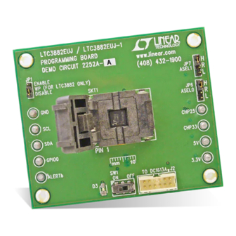
Page 66: Interfacing To The Dc1613
Linear Technology. A great deal of context ing parameters, as shown in Figure 55. The DC1613 I connections are opto-isolated from the host PC USB. The sensitive help is available within LTpowerPlay, along with several tutorials. - Page 67 LTC3882-1 APPLICATIONS INFORMATION SYSTEM TP0101K LT6703-2 102k –IN TP0101K – DD33 DD25 2.2µF 1µF LTC3882-1 2N2002 400mV REFERENCE CONTROLLER 4.7µF HEADER DD33 DD25 2.2µF 1µF ISOLATED 5V LTC3882-1 38821 F47 TO LTC DC1613 USB TO I C/SMBus/PMBus CONTROLLER Figure 47. DC1613 Connection (V Supply) ENBA STAT...
- Page 68 LTC3882-1 APPLICATIONS INFORMATION The frequency and phase are also set by EEPROM values. A loop crossover frequency of 100kHz provides good Assume that solution footprint or vertical clearance is an transient performance while still being well below the issue, so operating frequency will need to be increased switching frequency of the converter.
-
Page 69: Pmbus Command Details
LTC3882-1 PMBus COMMAND DETAILS (by functional groups) ADDRESSING AND WRITE PROTECT DATA DEFAULT COMMAND NAME CODE DESCRIPTION TYPE PAGED FORMAT UNITS NVM VALUE PAGE 0x00 Channel (page) presently selected for any R/W Byte 0x00 paged command. PAGE_PLUS_WRITE 0x05 Write a command directly to a specified page. W Block PAGE_PLUS_READ 0x06 Read a command directly from a specified... -
Page 70: Page_Plus_Read
LTC3882-1 PMBus COMMAND DETAILS (Addressing and Write Protect) PAGE_PLUS_READ The PAGE_PLUS_READ command provides the ability to set the page within a device, send a command and then read the data returned by the command, all in one communication packet . The value stored in the PAGE command is not affected by PAGE_PLUS_READ. -
Page 71: Mfr_Address
LTC3882-1 PMBus COMMAND DETAILS (Addressing and Write Protect) MFR_ADDRESS The MFR_ADDRESS command sets the seven bits of the PMBus device address for this unit (right justified). Setting this command to a value of 0x80 disables device-level addressing. The GLOBAL device addresses 0x5A and 0x5B cannot be disabled. -
Page 72: On, Off And Margin Control
LTC3882-1 PMBus COMMAND DETAILS (General Device Configuration) MFR_CONFIG_ALL_LTC3882-1 The MFR_CONFIG_ALL_LTC3882-1 command provides device-level configuration common to multiple LTC PMBus products. Bit Definitions: MEANING Enable fault logging. Ignore resistor configuration pins. Does not apply to ASEL0 or ASEL1. Disable CML fault for Quick Command message. Disable SYNC output. -
Page 73: Operation
LTC3882-1 PMBus COMMAND DETAILS (On, Off and Margin Control) OPERATION The OPERATION command is used to turn the PWM channel on and off in conjunction with RUN pin hardware control. This command may also be used to move the output voltage to margin levels. V changes commanded by OPERATION margin commands occur at the programmed VOUT_TRANSITION_RATE. -
Page 74: Pwm Configuration
LTC3882-1 PMBus COMMAND DETAILS (PWM Configuration) PWM CONFIGURATION DATA DEFAULT COMMAND NAME CODE DESCRIPTION TYPE PAGED FORMAT UNITS NVM VALUE FREQUENCY_SWITCH 0x33 PWM frequency control. R/W Word 500kHz 0xFBE8 MFR_PWM_CONFIG_LTC3882-1 0xF5 LTC3882-1 PWM configuration common to R/W Byte 0x14 both channels. MFR_CHAN_CONFIG_LTC3882-1 0xD0 LTC3882-1 channel-specific configuration. -
Page 75: Mfr_Pwm_Config_Ltc3882-1
LTC3882-1 PMBus COMMAND DETAILS (PWM Configuration) MFR_PWM_CONFIG_LTC3882-1 The MFR_PWM_CONFIG_LTC3882-1 command controls PWM-related clocking for the LTC3882-1. Both PWM chan- nels must be turned off by the RUNn pins, OPERATION command, or their combination, to process this command. If this command is sent while either PWM controller is operating, the LTC3882-1 will NACK the command byte, ignore the command and its data, and assert a BUSY fault. -
Page 76: Mfr_Chan_Config_Ltc3882-1
LTC3882-1 PMBus COMMAND DETAILS (PWM Configuration) MFR_CHAN_CONFIG_LTC3882-1 The MFR_CHAN_CONFIG_LTC3882-1 command provides per-channel configuration common to multiple LTC PMBus products. Bit Definitions: MEANING (Reserved). RUN pin control: 0: When the channel is commanded off, the associated RUN pin is pulsed low for TOFF_DELAY + TOFF_FALL + 136ms (or MFR_RESTART_DELAY, if longer) regardless of the state of bit 3. -
Page 77: Mfr_Pwm_Mode_Ltc3882-1
LTC3882-1 PMBus COMMAND DETAILS (PWM Configuration) MFR_PWM_MODE_LTC3882-1 The MFR_PWM_MODE_LTC3882-1 command sets important PWM controls for each channel. The addressed channel(s) must be turned off by its RUN pin, OPERATION command, or their combination, when this command is issued. Oth- erwise the LTC3882-1 will NACK the command byte, ignore the command and its data, and assert a BUSY fault. When bit 5 is cleared, the LTC3882-1 computes temperature in °C from ∆V measured by the ADC at the TSNSn pin as T = (G •... -
Page 78: Input Voltage And Limits
LTC3882-1 PMBus COMMAND DETAILS (Input Voltage and Limits) INPUT VOLTAGE AND LIMITS DATA DEFAULT COMMAND NAME CODE DESCRIPTION TYPE PAGED FORMAT UNITS NVM VALUE VIN_ON 0x35 Minimum input voltage to begin power R/W Word 6.5V conversion. 0xCB40 VIN_OFF 0x36 Decreasing input voltage at which power R/W Word 6.0V conversion stops. -
Page 79: Output Voltage And Limits
LTC3882-1 PMBus COMMAND DETAILS (Output Voltage and Limits) OUTPUT VOLTAGE AND LIMITS DATA DEFAULT COMMAND NAME CODE DESCRIPTION TYPE PAGED FORMAT UNITS NVM VALUE –12 VOUT_MODE 0x20 Output voltage format and exponent. R Byte 0x14 VOUT_COMMAND 0x21 Nominal V value. R/W Word 1.0V 0x1000... -
Page 80: Vout_Max
LTC3882-1 PMBus COMMAND DETAILS (Output Voltage and Limits) VOUT_MAX The VOUT_MAX command sets an upper limit, in volts, on the allowed value of any command that sets the output voltage, including VOUT_MARGIN_HIGH. Setting VOUT_MAX to a value greater than MFR_VOUT_MAX will result in a CML fault and VOUT_MAX will be set to the value of MFR_VOUT_MAX. -
Page 81: Vout_Ov_Warn_Limit
LTC3882-1 PMBus COMMAND DETAILS (Output Voltage and Limits) VOUT_OV_WARN_LIMIT The VOUT_OV_WARN_LIMIT command sets the value, in volts, of the output voltage measured by the ADC at the ± pins that causes an output overvoltage warning. If the VOUT_OV_WARN_LIMIT is exceeded, the device: SENSE •... -
Page 82: Output Current And Limits
LTC3882-1 PMBus COMMAND DETAILS (Output Current and Limits) OUTPUT CURRENT AND LIMITS DATA DEFAULT COMMAND NAME CODE DESCRIPTION TYPE PAGED FORMAT UNITS NVM VALUE ± IOUT_CAL_GAIN 0x38 Ratio of I voltage to sensed current. R/W Word mΩ 0.63mΩ SENSE 0xB285 MFR_IOUT_CAL_GAIN_TC 0xF6 Output current sense element temperature R/W Word... -
Page 83: Output Timing, Delays, And Ramping
LTC3882-1 PMBus COMMAND DETAILS (Output Timing, Delays, and Ramping) OUTPUT TIMING, DELAYS, AND RAMPING DATA DEFAULT COMMAND NAME CODE DESCRIPTION TYPE PAGED FORMAT UNITS NVM VALUE MFR_RESTART_DELAY 0xDC Minimum time RUN pin is held low by the R/W Word 500ms LTC3882-1. -
Page 84: Ton_Max_Fault_Limit
LTC3882-1 PMBus COMMAND DETAILS (Output Timing, Delays and Ramping) TON_MAX_FAULT_LIMIT The TON_MAX_FAULT_LIMIT command sets the maximum time, in milliseconds, the unit is allowed from the beginning of TON_RISE to power up the output without passing VOUT_UV_FAULT_LIMIT. A value of 0ms means there is no limit and the unit can attempt to bring up the output voltage indefinitely. -
Page 85: External Temperature And Limits
LTC3882-1 PMBus COMMAND DETAILS (External Temperature and Limits) EXTERNAL TEMPERATURE AND LIMITS DATA DEFAULT COMMAND NAME CODE DESCRIPTION TYPE PAGED FORMAT UNITS NVM VALUE MFR_TEMP_1_GAIN 0xF8 Set slope for external temperature R/W Word calculations. 0x4000 MFR_TEMP_1_OFFSET 0xF9 Offset addend for external temperature R/W Word °C or V calculations. -
Page 86: Status Reporting
LTC3882-1 PMBus COMMAND DETAILS (External Temperature Limits) UT_FAULT_LIMIT The UT_FAULT_LIMIT command sets the value of sensed external temperature, in degrees Celsius, which causes an undertemperature fault. This command has two data bytes in Linear_5s_11s format. STATUS REPORTING DATA DEFAULT COMMAND NAME CODE DESCRIPTION TYPE PAGED... -
Page 87: Status_Word
LTC3882-1 PMBus COMMAND DETAILS (Status Reporting) STATUS_WORD The STATUS_WORD command returns a two-byte summary of the channel's fault condition. The low byte of the STA- TUS_WORD is the same as the STATUS_BYTE command. STATUS_WORD High Byte Message Contents: STATUS BIT NAME MEANING VOUT An output voltage fault or warning has occurred. -
Page 88: Status_Input
LTC3882-1 PMBus COMMAND DETAILS (Status Reporting) STATUS_INPUT The STATUS_INPUT command returns one byte of V (VINSNS) status information. STATUS_INPUT Message Contents: MEANING overvoltage fault. Not supported (LTC3882-1 returns 0). undervoltage warning. Not supported (LTC3882-1 returns 0). Unit off for insufficient V Not supported (LTC3882-1 returns 0). -
Page 89: Status_Mfr_Specific
LTC3882-1 PMBus COMMAND DETAILS (Status Reporting) STATUS_MFR_SPECIFIC The STATUS_MFR_SPECIFIC command returns one byte with LTC3882-1-specific status information. STATUS_MFR_SPECIFIC Message Contents: MEANING Internal temperature fault (>160°C). Internal temperature warning (>130°C). EEPROM CRC error. Internal PLL unlocked. Fault log present. Not supported (LTC3882-1 returns 0). Output short cycled. -
Page 90: Mfr_Common
LTC3882-1 PMBus COMMAND DETAILS (Status Reporting) MFR_COMMON The MFR_COMMON command contains status bits that are common to multiple LTC PMBus products. MFR_COMMON Message Contents: MEANING LTC3882-1 not forcing ALERT low. LTC3882-1 not BUSY. LTC3882-1 calculations not pending. LTC3882-1 output not in transition. LTC3882-1 EEPROM initialized. -
Page 91: Telemetry
LTC3882-1 PMBus COMMAND DETAILS (Status Reporting) TELEMETRY DATA DEFAULT COMMAND NAME CODE DESCRIPTION TYPE PAGED FORMAT UNITS NVM VALUE READ_VIN 0x88 Measured V R Word MFR_VIN_PEAK 0xDE Maximum V measurement since last R Word MFR_CLEAR_PEAKS. READ_VOUT 0x8B Measured V R Word MFR_VOUT_PEAK 0xDD Maximum V measurement since last... -
Page 92: Read_Iout
LTC3882-1 PMBus COMMAND DETAILS (Telemetry) READ_IOUT The READ_IOUT command returns the output current in amperes. This value is computed from: ± • The differential voltage measured across the I pins SENSE • The IOUT_CAL_GAIN value • The MFR_IOUT_CAL_GAIN_TC value • The READ_TEMPERATURE_1 value •... -
Page 93: Mfr_Temperature_2_Peak
LTC3882-1 PMBus COMMAND DETAILS (Telemetry) MFR_TEMPERATURE_2_PEAK The MFR_TEMPERATURE_2_PEAK command reports the highest temperature, in degrees Celsius, calculated for READ_TEMPERATURE_2. This peak value can be reset by a MFR_CLEAR_PEAKS command. This read-only command has two data bytes in Linear_5s_11s format. READ_DUTY_CYCLE The READ_DUTY_CYCLE command returns the duty cycle of the PWM control in percent. -
Page 94: Fault Response And Communication
LTC3882-1 PMBus COMMAND DETAILS (Fault Response and Communication) FAULT RESPONSE AND COMMUNICATION DATA DEFAULT COMMAND NAME CODE DESCRIPTION TYPE PAGED FORMAT UNITS NVM VALUE VIN_OV_FAULT_RESPONSE 0x56 V overvoltage fault response. R/W Byte 0x80 VOUT_OV_FAULT_RESPONSE 0x41 V overvoltage fault response. R/W Byte 0xB8 VOUT_UV_FAULT_RESPONSE 0x45 V... -
Page 95: Vout_Ov_Fault_Response
LTC3882-1 PMBus COMMAND DETAILS (Fault Response and Communication) VOUT_OV_FAULT_RESPONSE The VOUT_OV_FAULT_RESPONSE command instructs the device on what action to take in response to an output overvoltage fault. The format for this command is given in Table 12. The device also: •... -
Page 96: Iout_Oc_Fault_Response
LTC3882-1 PMBus COMMAND DETAILS (Fault Response and Communication) IOUT_OC_FAULT_RESPONSE The IOUT_OC_FAULT_RESPONSE command instructs the device on what action to take in response to an output overcurrent fault. The device also: • Sets the IOUT_OC Bit in the STATUS_BYTE • Sets the IOUT Bit in the STATUS_WORD •... -
Page 97: Ot_Fault_Response
LTC3882-1 PMBus COMMAND DETAILS (Fault Response and Communication) OT_FAULT_RESPONSE The OT_FAULT_RESPONSE command instructs the device on what action to take in response to an overtemperature fault. The format for this command is given in Table 13. The device also: • Sets the TEMPERATURE Bit in the STATUS_BYTE •... -
Page 98: Ton_Max_Fault_Response
LTC3882-1 PMBus COMMAND DETAILS (Fault Response and Communication) TON_MAX_FAULT_RESPONSE The TON_MAX_FAULT_RESPONSE command instructs the device on what action to take in response to a TON_MAX fault. The format for this command is given in Table 13. The device also: • Sets the VOUT Bit in the STATUS_WORD •... -
Page 99: Mfr_Fault_Propagate_Ltc3882-1
LTC3882-1 PMBus COMMAND DETAILS (Fault Response and Communication) Figure 51 shows an example of the Write Word format used to set an ALERT mask, in this case without PEC. The bits in the mask byte align with bits in the specified status register. For example, if the STATUS_TEMPERATURE command code is sent in the first data byte, and the mask byte contains 0x40, then a subsequent External Overtemperature Warn- ing would still set bit 6 of STATUS_TEMPERATURE but not assert ALERT. -
Page 100: Mfr_Fault_Response
LTC3882-1 PMBus COMMAND DETAILS (Fault Response and Communication) Supported Values: PROPAGATED CONDITION Waiting for V decay before restart. short cycled (automatically deasserted 120ms after V is fully OFF). TON_MAX_FAULT_LIMIT exceeded. (Reserved, must be set to 0). MFR_OT_FAULT_LIMIT exceeded. (Reserved, must be set to 0). (Reserved, must be set to 0). -
Page 101: Mfr_Fault_Log
LTC3882-1 PMBus COMMAND DETAILS (Fault Response and Communication) MFR_FAULT_LOG The MFR_FAULT_LOG command allows the contents of the fault log to be read. This log is created with a MFR_FAULT_LOG_STORE command or at the first fault occurrence after a CLEAR_FAULTS or MFR_FAULT_LOG_CLEAR command. -
Page 102: Eeprom User Access
LTC3882-1 PMBus COMMAND DETAILS (EEPROM User Access) EEPROM USER ACCESS DATA DEFAULT COMMAND NAME CODE DESCRIPTION TYPE PAGED FORMAT UNITS NVM VALUE STORE_USER_ALL 0x15 Store entire operating memory in EEPROM. Send Byte RESTORE_USER_ALL 0x16 Restore entire operating memory from Send Byte EEPROM. -
Page 103: Mfr_Fault_Log_Store
LTC3882-1 PMBus COMMAND DETAILS (EEPROM User Access) MFR_FAULT_LOG_STORE The MFR_FAULT_LOG_STORE command forces a data log to be written to internal EEPROM as if a fault event had occurred. This command will generate a CML fault if the Enable Fault Logging bit is cleared in MFR_CONFIG_ALL_LTC3882-1. This write-only command has no data bytes. -
Page 104: Typical Applications
LTC3882-1 TYPICAL APPLICATIONS Rev A For more information www.analog.com... - Page 105 LTC3882-1 TYPICAL APPLICATIONS Rev A For more information www.analog.com...
-
Page 106: Package Description
LTC3882-1 PACKAGE DESCRIPTION Please refer to http://www.linear.com/designtools/packaging/ for the most recent package drawings. UJ Package 40-Lead Plastic QFN (6mm × 6mm) (Reference LTC DWG # 05-08-1728 Rev Ø) 0.70 ±0.05 6.50 ±0.05 5.10 ±0.05 4.42 ±0.05 4.50 ±0.05 (4 SIDES) 4.42 ±0.05 PACKAGE OUTLINE 0.25 ±0.05... -
Page 107: Revision History
LTC3882-1 REVISION HISTORY DATE DESCRIPTION PAGE NUMBER 04/18 Added ECC 1, 17, 24 Reduced initialization time 5, 19 Reduced conversion time Rev A Information furnished by Analog Devices is believed to be accurate and reliable. However, no responsibility is assumed by Analog Devices for its use, nor for any infringements of patents or other rights of third parties that may result from its use. -
Page 108: Typical Application
LTC3882-1 TYPICAL APPLICATION 7V TO 14V 330µF 100nF BIAS ×2 +5V INPUT SUPPLY 1µF 2.2µF DD33 DD25 INPUT SUPPLY +5V TO +12V 2.2µF 1µF 4.7µF 4.99k 1µF 4.99k 4.99k VINSNS 22µF DD33 DD25 ×2 PHASE GH CGND GND BOOT V SMOD PWM0 PWM0...
Need help?
Do you have a question about the Analog Devices LTC3882-1 and is the answer not in the manual?
Questions and answers