
Subscribe to Our Youtube Channel
Related Manuals for Texas Instruments ADC12DJ5200RF


Summary of Contents for Texas Instruments ADC12DJ5200RF
- Page 1 ADC12DJ5200RF Evaluation Module User's Guide Literature Number: SLAU640 April 2019...
-
Page 2: Table Of Contents
B.2.2 Onboard Clocking Option ................B.2.3 External Reference Clocking Option ........................Signal Routing ......................Signal Routing ........................Analog Inputs ......................Jumpers and LEDs ......................Jumper settings Contents SLAU640 – April 2019 Submit Documentation Feedback Copyright © 2019, Texas Instruments Incorporated... - Page 3 ......................4-2. Low-Level Controls ......................5-1. Troubleshooting .................. C-1. ADCxxDJxx00RFEVM Signal Routing ......................D-1. Analog Input Path ......................E-1. Jumper Settings ......................... E-2. LEDs SLAU640 – April 2019 List of Figures Submit Documentation Feedback Copyright © 2019, Texas Instruments Incorporated...
-
Page 4: Preface
ADC12DJ5200RF evaluation board is referred to as the EVM and the ADC12DJ5200RF device is referred to as the ADC device. This document also includes an electrical schematic, printed circuit board (PCB) layout drawings, and a parts list for the EVM. -
Page 5: Introduction
SLAU640 – April 2019 Introduction The ADC12DJ5200RFEVM is an evaluation board used to evaluate the ADC12DJ5200RF analog-to- digital converters (ADC) from Texas Instruments. The ADC12DJ5200RFis a dual-channel, 12-bit ADC, capable of operating at sampling rates up to 5.2 Giga-samples per second (GSPS) in dual-channel mode, or 10.4 GSPS in single-channel mode. -
Page 6: Evm Orientation
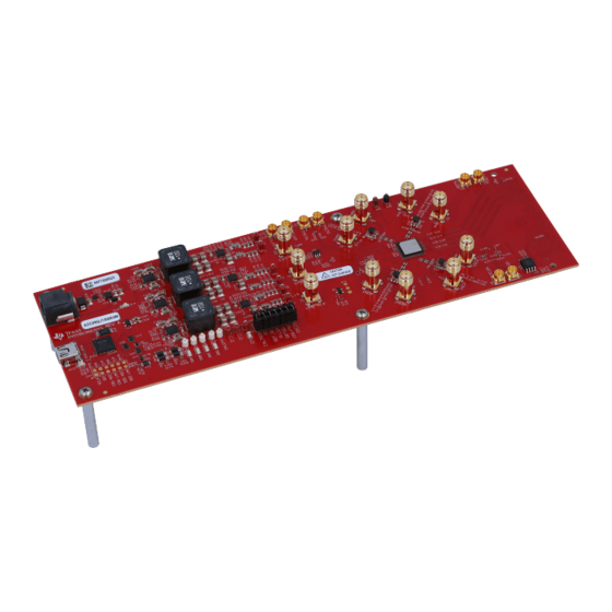
( J17 ) Power (DC/DC DQG /'2¶V) Connector +12V DC ADC12DJ5200RF EVM top side ADC12DJ5200RF EVM top side with ADC12DJ5200RF EVM bottom side without heat sink installed heat sink installed Copyright © 2016, Texas Instruments Incorporated Figure 1-1. EVM Orientation The digital data from the ADC12DJ5200RFEVM board is quickly and easily captured with the TSW14J57EVM data capture boards. -
Page 7: Equipment
External Reference Clock ( J17 ) Mini USB Connector +12V DC ( J20 ) ( J14 ) Copyright © 2016, Texas Instruments Incorporated Figure 2-1. EVM Feature Locations SLAU640 – April 2019 Equipment Submit Documentation Feedback Copyright © 2019, Texas Instruments Incorporated... -
Page 8: Required Equipment
TSW14J57EVM data capture board and related items • High-Speed Data Converter Pro software. Also install the HSDCpro Patch v5.00.02.exe to download ADC12DJ5200RF INI files to the PC. Make sure the install location matches Figure 2-2. Copyright © 2016, Texas Instruments Incorporated Figure 2-2. - Page 9 GUI using JMODE and the sampling frequency (Fs) entered by the user. The reference clock generator and device clock generator must be frequency- locked using a common 10-MHz reference. SLAU640 – April 2019 Equipment Submit Documentation Feedback Copyright © 2019, Texas Instruments Incorporated...
-
Page 10: Setup Procedure
1. Download the Configuration GUI software from the EVM tool folder at ADC12DJ5200RF GUI. 2. Extract files from the .zip file. 3. Run the executable file (setup.exe), and follow the instructions. Setup Procedure SLAU640 – April 2019 Submit Documentation Feedback Copyright © 2019, Texas Instruments Incorporated... -
Page 11: Connect The Evm And Tsw14J57Evm
Do not turn on the RF output of any signal generator at this time. When using the ADC in single-input mode, the device uses both edges of DEVCLK for sampling. SLAU640 – April 2019 Setup Procedure Submit Documentation Feedback Copyright © 2019, Texas Instruments Incorporated... -
Page 12: Turn On The Tsw14J57Evm Power And Connect To The Pc
Open the ADC12DJ5200RFEVM GUI and Program the ADC and Clocks The Device Configuration GUI is installed separately from the HSDC Pro installation and is a stand-alone GUI. Figure 3-2. Configuration GUI EVM Tab Setup Procedure SLAU640 – April 2019 Submit Documentation Feedback Copyright © 2019, Texas Instruments Incorporated... -
Page 13: 3.10 Calibrate The Adc Device On The Evm
EVM features with user-friendly controls and a low-level tab for directly configuring the registers. The EVM has three configurable devices, namely the ADC12DJ5200RF, LMK04828, LMK61E2, and LMX2594. The register map for each device is provided in the device data sheet (ADC12DJ5200RF 10.4-GSPS Single Channel or 5.2-GSPS Dual Channel, 12-bit,... -
Page 14: 3.11 Open The Hsdc Software And Load The Fpga Image To The Tsw14J57Evm
ADC, or after exiting the power-down mode. See the ADC12DJ5200RF device data sheet, (SLVSEN9) for details regarding the necessary calibration sequence. 3. To enable background calibration, use the following steps: •... -
Page 15: High Speed Data Converter Pro (Hsdc) Gui
The HSDC Pro GUI will calculate the ADC Output Data Rate based on these inputs. The Fundamental and Harmonic frequency locations will also be calculated and identified in the FFT display. SLAU640 – April 2019 Setup Procedure Submit Documentation Feedback Copyright © 2019, Texas Instruments Incorporated... -
Page 16: Additional Device Parameters Dialog Box
Capture Data Using the HSDC Pro Software www.ti.com Figure 3-5. Additional Device Parameters Dialog Box Setup Procedure SLAU640 – April 2019 Submit Documentation Feedback Copyright © 2019, Texas Instruments Incorporated... -
Page 17: Device Configuration
JESD204C settings. Once the settings are changed, re-enable the JESD204 block. Tab Organization Control of the ADC device features are available in the EVM, Control, JESD204C, NCO Configuration tabs. SLAU640 – April 2019 Device Configuration Submit Documentation Feedback Copyright © 2019, Texas Instruments Incorporated... -
Page 18: Low-Level Control
Perform a generic read or write command to the device shown in the Block drop-down box using read or write register buttons the address and write data information Figure 4-1. Low-Level Register Control Tab Device Configuration SLAU640 – April 2019 Submit Documentation Feedback Copyright © 2019, Texas Instruments Incorporated... -
Page 19: Troubleshooting The Adc12Dj5200Rfevm
• Check that the spectral analysis parameters are properly configured. performance • Verify that bandpass filters are used in the clock and input signal paths and that low-noise signal sources are used. SLAU640 – April 2019 Troubleshooting the ADC12DJ5200RFEVM Submit Documentation Feedback Copyright © 2019, Texas Instruments Incorporated... -
Page 20: A References
• LMX2594 data sheet • FTDI USB to Serial Driver Installation Manual (www.ftdichip.com/Support/Documents/InstallGuides.htm) TSW14J57EVM Operation Refer to the TSW14J57EVM user guide for configuration and status information. References SLAU640 – April 2019 Submit Documentation Feedback Copyright © 2019, Texas Instruments Incorporated... -
Page 21: Bhsdc Pro Settings For Optional Adc Device Configuration
SYSREF frequency must also be programmed to a compatible frequency. Ensure that the K value complies with the K Min and Step values for the selected JMODE. Refer to the ADC12DJ5200RF operating modes table in the ADC12DJ5200RF data sheet. -
Page 22: External Clocking Option (Default)
SYSREF CLKIN0 32.5 MHz SDCLKx SDCLKx FPGA_SYSREF External Clock CLKIN1 DCLKx FPGA_CLK[3:0] Figure B-1. ADC12DJ5200RFEVM Clocking System Block Diagram HSDC Pro Settings for Optional ADC Device Configuration SLAU640 – April 2019 Submit Documentation Feedback Copyright © 2019, Texas Instruments Incorporated... -
Page 23: Onboard Clocking Option
SYSREFREQ RFOUTB SYSREF CLKIN0 SDCLKx SDCLKx FPGA_SYSREF Onboard Clock CLKIN1 DCLKx FPGA_CLK[3:0] Figure B-2. Onboard Clocking System Block Diagram SLAU640 – April 2019 HSDC Pro Settings for Optional ADC Device Configuration Submit Documentation Feedback Copyright © 2019, Texas Instruments Incorporated... -
Page 24: External Reference Clocking Option
FPGA_SYSREF Referencel Clock CLKIN1 DCLKx FPGA_CLK[3:0] Figure B-3. External Reference Clocking System Block Diagram Figure B-4. External Clock Configuration HSDC Pro Settings for Optional ADC Device Configuration SLAU640 – April 2019 Submit Documentation Feedback Copyright © 2019, Texas Instruments Incorporated... -
Page 25: Onboard Clocking Configuration
Customizing the EVM for Optional Clocking Support www.ti.com Figure B-5. Onboard Clocking Configuration SLAU640 – April 2019 HSDC Pro Settings for Optional ADC Device Configuration Submit Documentation Feedback Copyright © 2019, Texas Instruments Incorporated... -
Page 26: C Signal Routing
DP9_M2C Y14,Y15 DP12_M2C_INV Z16,Z17 DP13_M2C_INV Y18,Y19 DP14_M2C_INV Y22,Y23 DP15_M2C_INV Red items with _INV in the signal name are inverted with respect to standard FMC polarity. Signal Routing SLAU640 – April 2019 Submit Documentation Feedback Copyright © 2019, Texas Instruments Incorporated... -
Page 27: D Analog Inputs
S/E Balun AC (default) INA(J4), INB(J7) 0 Ω (500kHz to 9GHz) INAP(J5), INAM(J3), Differential 0.1 µF INBP(J6), INBM(J8) Differential INAP, INAM, INBP, INBM 0 Ω SLAU640 – April 2019 Analog Inputs Submit Documentation Feedback Copyright © 2019, Texas Instruments Incorporated... -
Page 28: Analog Input Path
Appendix D www.ti.com Figure D-1. Analog Input Path Analog Inputs SLAU640 – April 2019 Submit Documentation Feedback Copyright © 2019, Texas Instruments Incorporated... -
Page 29: D-2. 3 Db Attenuation Pad
A 3dB attenuation pad is added between the inputs and the ADC. The 3 dB pad helps with the flatness of the frequency response. Figure D-2. 3 dB attenuation pad SLAU640 – April 2019 Analog Inputs Submit Documentation Feedback Copyright © 2019, Texas Instruments Incorporated... -
Page 30: E Jumpers And Leds
FTDI IC is controlling the devices on the EVMs Table E-2. LEDs Label Function High temp indicator High input power on channel A High input power on channel B Jumpers and LEDs SLAU640 – April 2019 Submit Documentation Feedback Copyright © 2019, Texas Instruments Incorporated... - Page 31 TI products. TI’s provision of these resources does not expand or otherwise alter TI’s applicable warranties or warranty disclaimers for TI products. Mailing Address: Texas Instruments, Post Office Box 655303, Dallas, Texas 75265 Copyright © 2019, Texas Instruments Incorporated...
Need help?
Do you have a question about the ADC12DJ5200RF and is the answer not in the manual?
Questions and answers