Table of Contents
Advertisement
Quick Links
ADS42JB46, ADS42JB49, and ADS42JB69 Evaluation
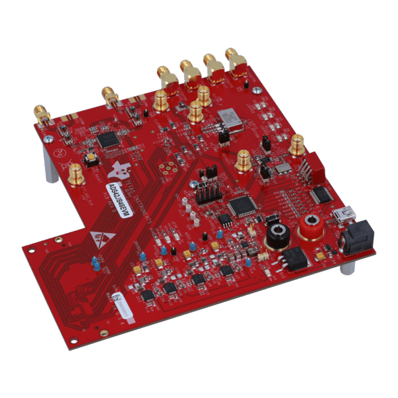
This document outlines the basic steps and functions that are required to ensure the proper operation of
the Texas Instruments (TI) ADS42JB46, ADS42JB49, and ADS42JB69 Evaluation Modules (hereafter in
this document, ADS42JBxxEVM or EVM). The EVM package includes an ADS42JBxxEVM, a 5-VDC
power supply, and a mini-USB cable. This EVM is designed to be used with the TSW14J5xEVM (a
JESD204B data capture card). The ADS42JBxx EVM can also be connected to all FPGA development
platforms with an FMC connector for evaluation. The ADS42JBxxEVM includes either an ADS42JB49 (14-
bit), or ADS42JB69 (16-bit) dual-channel, 250-MSPS, or an ADS42JB46 (14-bit) dual channel, 160-MSPS
analog-to-digital converter. The EVM also includes a TI LMK04828 clock jitter cleaner to provide a low
jitter/phase noise sampling clock to the ADC. This user's guide outlines the steps to quickly evaluate the
performance of the ADS42JBxx ADC by capturing and displaying signal waveforms using the
TSW14J5xEVM and the High Speed Data Converter Pro GUI software. The EVM schematics, BOMs, and
layout files are found in the design package under the ADS42JBxxEVM product folder available on
http://www.ti.com.
spacer
spacer
...................................................................................................................
1
1.1
Overview
1.2
2
2.1
2.2
3
3.1
3.2
3.3
LMK Controls
3.4
Low Level View
1
Block Diagram of the ADS42JBxxEVM
2
EVM Hardware Setup
3
ADS42JBxx EVM GUI Setup
4
HSDC Pro Software Setup
5
ADC Data Capture, 25 MHz Sinusoid, 250 MSPS Sampling Rate
6
Top-Level Block Diagram Window of the ADS42JBxx GUI
7
8
9
10
11
12
Low Level View
SLAU467D - November 2012 - Revised February 2017
Submit Documentation Feedback
.............................................................................................................
.......................................................................................................
.............................................................................................................
...........................................................................................................
..........................................................................................................
............................................................................................
......................................................................................................
......................................................................................................
....................................................................................................
...................................................................................
.......................................................................................................
...............................................................................................
.................................................................................................
.................................................................................................
...............................................................................
........................................................................................
.............................................................................................................
Copyright © 2012-2017, Texas Instruments Incorporated
SLAU467D - November 2012 - Revised February 2017
Contents
..............................................................
List of Figures
...................................................
............................................................
........................................................................
........................................................
ADS42JB46, ADS42JB49, and ADS42JB69 Evaluation Module
User's Guide
Module
2
2
3
4
4
5
9
9
10
13
17
3
5
6
7
8
9
10
13
14
15
16
17
1
Advertisement
Table of Contents

Related Manuals for Texas Instruments ADS42JB46


Summary of Contents for Texas Instruments ADS42JB46
-
Page 1: Table Of Contents
FMC connector for evaluation. The ADS42JBxxEVM includes either an ADS42JB49 (14- bit), or ADS42JB69 (16-bit) dual-channel, 250-MSPS, or an ADS42JB46 (14-bit) dual channel, 160-MSPS analog-to-digital converter. The EVM also includes a TI LMK04828 clock jitter cleaner to provide a low jitter/phase noise sampling clock to the ADC. -
Page 2: Slau467D – November 2012 – Revised February
(ADC) with a buffered analog input and outputs featuring a JESD204B interface. The ADS42JB46 (14-bit) is a low power 160-MSPS ADC version of the same family of ADC's. The EVM has transformer-coupled analog inputs accommodating a wide range of signal sources and frequencies. The... -
Page 3: Introduction
ADS42JBxxEVM SYNC 4 TX ADS42JBxx LMK04828 JESD204B 5VDC Clock Generator Figure 1. Block Diagram of the ADS42JBxxEVM SLAU467D – November 2012 – Revised February 2017 ADS42JB46, ADS42JB49, and ADS42JB69 Evaluation Module Submit Documentation Feedback Copyright © 2012–2017, Texas Instruments Incorporated... -
Page 4: Software Control
This section provides installation instructions for the ADS42JBxx GUI and descriptions of the various controls. Please note, any illustration and textual references to ADS42JB69 or ADS42JBx9 in this section apply to the ADS42JB46 as well. Installation Instructions for ADS42JBxxEVM GUI 1. -
Page 5: Quick Start
5. IMPORTANT: Push the hardware reset (SW1) on the ADS42JBxx EVM board. This is required each time the EVM is powered up to ensure proper operation. SLAU467D – November 2012 – Revised February 2017 ADS42JB46, ADS42JB49, and ADS42JB69 Evaluation Module Submit Documentation Feedback Copyright © 2012–2017, Texas Instruments Incorporated... - Page 6 The configuration file sets the ADC up for Fsampling = 250 MHz, lane rate = 2.5 GHz, L = 4, M = 2, F = 1. ADS42JB46, ADS42JB49, and ADS42JB69 Evaluation Module SLAU467D – November 2012 – Revised February 2017 Submit Documentation Feedback Copyright ©...
- Page 7 With no input signal connected to the ADC inputs, the captured noise floor of the ADC should look like Figure SLAU467D – November 2012 – Revised February 2017 ADS42JB46, ADS42JB49, and ADS42JB69 Evaluation Module Submit Documentation Feedback Copyright © 2012–2017, Texas Instruments Incorporated...
- Page 8 Refer to the HSDC Pro GUI users guide (SLWU087) for more details. Copyright © 2017, Texas Instruments Incorporated Figure 5. ADC Data Capture, 25 MHz Sinusoid, 250 MSPS Sampling Rate ADS42JB46, ADS42JB49, and ADS42JB69 Evaluation Module SLAU467D – November 2012 – Revised February 2017 Submit Documentation Feedback...
-
Page 9: Software Operation
Detailed descriptions for each screen of the GUI are given in this section. Please refer to the datasheet (ADS42JB46 - SLAS621, ADS42JBx9 - SLAS900) for more detailed explanations of the register fields. -
Page 10: Adc Controls
Copyright © 2017, Texas Instruments Incorporated Figure 7. ADC Controls Window of the ADS42JBxx GUI ADS42JB46, ADS42JB49, and ADS42JB69 Evaluation Module SLAU467D – November 2012 – Revised February 2017 Submit Documentation Feedback Copyright © 2012–2017, Texas Instruments Incorporated... - Page 11 Ch B Fast OVR Voltage Overrange indication channel B (Ch B FS Voltage × [Fast OVR Threshold / 127]) SLAU467D – November 2012 – Revised February 2017 ADS42JB46, ADS42JB49, and ADS42JB69 Evaluation Module Submit Documentation Feedback Copyright © 2012–2017, Texas Instruments Incorporated...
- Page 12 LMFC counter LMFC Count Initial Value The initial value that the LMFC count resets to ADS42JB46, ADS42JB49, and ADS42JB69 Evaluation Module SLAU467D – November 2012 – Revised February 2017 Submit Documentation Feedback Copyright © 2012–2017, Texas Instruments Incorporated...
-
Page 13: Lmk04828 Outputs Control Window Of The Ads42Jbxx Gui
(ppm) is too large. Copyright © 2017, Texas Instruments Incorporated Figure 8. LMK04828 Outputs Control Window of the ADS42JBxx GUI SLAU467D – November 2012 – Revised February 2017 ADS42JB46, ADS42JB49, and ADS42JB69 Evaluation Module Submit Documentation Feedback Copyright © 2012–2017, Texas Instruments Incorporated... -
Page 14: Lmk04828 Pll2 Controls
Copyright © 2017, Texas Instruments Incorporated Figure 9. LMK04828 PLL2 Controls ADS42JB46, ADS42JB49, and ADS42JB69 Evaluation Module SLAU467D – November 2012 – Revised February 2017 Submit Documentation Feedback Copyright © 2012–2017, Texas Instruments Incorporated... -
Page 15: Lmk04828 Sysref And Sync Settings
The SYNC event must occur for digital delay values to take effect. Copyright © 2017, Texas Instruments Incorporated Figure 10. LMK04828 SYSREF and SYNC Settings SLAU467D – November 2012 – Revised February 2017 ADS42JB46, ADS42JB49, and ADS42JB69 Evaluation Module Submit Documentation Feedback Copyright © 2012–2017, Texas Instruments Incorporated... -
Page 16: Lmk04828 Output Clock Settings
14 outputs can be individually configured as high performance outputs for traditional clocking systems. Copyright © 2017, Texas Instruments Incorporated Figure 11. LMK04828 Output Clock Settings ADS42JB46, ADS42JB49, and ADS42JB69 Evaluation Module SLAU467D – November 2012 – Revised February 2017 Submit Documentation Feedback Copyright © 2012–2017, Texas Instruments Incorporated... - Page 17 Low Level View tab. Copyright © 2017, Texas Instruments Incorporated Figure 12. Low Level View SLAU467D – November 2012 – Revised February 2017 ADS42JB46, ADS42JB49, and ADS42JB69 Evaluation Module Submit Documentation Feedback Copyright © 2012–2017, Texas Instruments Incorporated...
-
Page 18: Revision History
Updated images and text in the Software Control section due to software changes.......... • Updated images and text in the Software Operation section due to software changes Revision History SLAU467D – November 2012 – Revised February 2017 Submit Documentation Feedback Copyright © 2012–2017, Texas Instruments Incorporated... - Page 19 STANDARD TERMS FOR EVALUATION MODULES Delivery: TI delivers TI evaluation boards, kits, or modules, including any accompanying demonstration software, components, and/or documentation which may be provided together or separately (collectively, an “EVM” or “EVMs”) to the User (“User”) in accordance with the terms set forth herein.
- Page 20 FCC Interference Statement for Class B EVM devices NOTE: This equipment has been tested and found to comply with the limits for a Class B digital device, pursuant to part 15 of the FCC Rules. These limits are designed to provide reasonable protection against harmful interference in a residential installation.
- Page 21 【無線電波を送信する製品の開発キットをお使いになる際の注意事項】 開発キットの中には技術基準適合証明を受けて いないものがあります。 技術適合証明を受けていないもののご使用に際しては、電波法遵守のため、以下のいずれかの 措置を取っていただく必要がありますのでご注意ください。 1. 電波法施行規則第6条第1項第1号に基づく平成18年3月28日総務省告示第173号で定められた電波暗室等の試験設備でご使用 いただく。 2. 実験局の免許を取得後ご使用いただく。 3. 技術基準適合証明を取得後ご使用いただく。 なお、本製品は、上記の「ご使用にあたっての注意」を譲渡先、移転先に通知しない限り、譲渡、移転できないものとします。 上記を遵守頂けない場合は、電波法の罰則が適用される可能性があることをご留意ください。 日本テキサス・イ ンスツルメンツ株式会社 東京都新宿区西新宿6丁目24番1号 西新宿三井ビル 3.3.3 Notice for EVMs for Power Line Communication: Please see http://www.tij.co.jp/lsds/ti_ja/general/eStore/notice_02.page 電力線搬送波通信についての開発キットをお使いになる際の注意事項については、次のところをご覧ください。http:/ /www.tij.co.jp/lsds/ti_ja/general/eStore/notice_02.page 3.4 European Union 3.4.1 For EVMs subject to EU Directive 2014/30/EU (Electromagnetic Compatibility Directive): This is a class A product intended for use in environments other than domestic environments that are connected to a low-voltage power-supply network that supplies buildings used for domestic purposes.
- Page 22 Notwithstanding the foregoing, any judgment may be enforced in any United States or foreign court, and TI may seek injunctive relief in any United States or foreign court. Mailing Address: Texas Instruments, Post Office Box 655303, Dallas, Texas 75265 Copyright © 2017, Texas Instruments Incorporated...
- Page 23 IMPORTANT NOTICE FOR TI DESIGN INFORMATION AND RESOURCES Texas Instruments Incorporated (‘TI”) technical, application or other design advice, services or information, including, but not limited to, reference designs and materials relating to evaluation modules, (collectively, “TI Resources”) are intended to assist designers who are developing applications that incorporate TI products;...
- Page 24 Mouser Electronics Authorized Distributor Click to View Pricing, Inventory, Delivery & Lifecycle Information: Texas Instruments ADS42JB69EVM ADS42JB46EVM...
Need help?
Do you have a question about the ADS42JB46 and is the answer not in the manual?
Questions and answers