Table of Contents
Advertisement
Quick Links
SUPER CHARGE PUMP DC-TO-DC VOLTAGE CONVERTER
FEATURES
Oscillator boost from 10kHz to 45kHz
Converts +5V Logic Supply to
Wide Input Voltage Range .................... 1.5V to 12V
Efficient Voltage Conversion ......................... 99.9%
Excellent Power Efficiency ............................... 98%
Low Power Supply .............................. 80
Low Cost and Easy to Use
— Only Two External Capacitors Required
Available in Small Outline (SOIC) Package
Improved ESD Protection ..................... Up to 10kV
No External Diode Required for High Voltage
Operation
ORDERING INFORMATION
Part No.
Package
TC7660SCOA
8-Pin SOIC
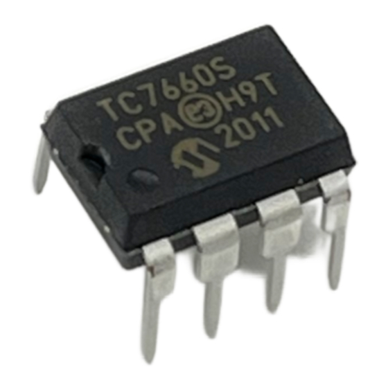
TC7660SCPA
8-Pin Plastic DIP
TC7660SEJA
8-Pin CerDIP
TC7660SEOA
8-Pin SOIC
TC7660SEPA
8-Pin Plastic DIP
TC7660SMJA
8-Pin CerDIP
TC7660EV
Evaluation Kit for
Charge Pump Family
FUNCTIONAL BLOCK DIAGRAM
1
BOOST
7
OSC
6
LV
© 2001 Microchip Technology Inc.
DS21467A
±
5V System
µ
A @ 5 V
Temperature
Range
0°C to +70°C
0°C to +70°C
– 40°C to +85°C
– 40°C to +85°C
– 40°C to +85°C
– 55°C to +125°C
RC
÷ 2
OSCILLATOR
INTERNAL
VOLTAGE
REGULATOR
TC7660S
EVALUATION
AVAILABLE
GENERAL DESCRIPTION
The TC7660S is a pin-compatible upgrade to the Indus-
try standard TC7660 charge pump voltage converter. It
converts a +1.5V to +12V input to a corresponding -1.5V to
-12V output using only two low-cost capacitors, eliminating
inductors and their associated cost, size and EMI. Added
features include an extended supply range to 12V, and a
IN
frequency boost pin for higher operating frequency, allowing
the use of smaller external capacitors.
The on-board oscillator operates at a nominal frequency
of 10kHz. Frequency is increased to 45kHz when pin 1 is
connected to V+. Operation below 10kHz (for lower supply
current applications) is possible by connecting an external
capacitor from OSC to ground (with pin 1 open).
The TC7660S is available in both 8-pin DIP and 8-pin
small outline (SOIC) packages in commercial and extended
temperature ranges.
PIN CONFIGURATION (DIP AND SOIC)
Boost
1
CAP +
2
TC7660SCPA
GND
3
TC7660SEJA
CAP –
4
TC7660SEPA
V + CAP +
8
2
VOLTAGE–
LEVEL
TRANSLATOR
3
GND
KIT
+
Boost
8
1
V
CAP +
7
2
OSC
LOW
GND
TC7660SCOA
6
3
VOLTAGE (LV)
TC7660SEOA
–
5
V OUT
CAP
4
4
CAP –
5
V OUT
LOGIC
NETWORK
TC7660S
+
8
V
OSC
7
LOW
6
VOLTAGE (LV)
V OUT
5
TC7660S-14 9/16/96
Advertisement
Table of Contents

Related Manuals for Microchip Technology TC7660S Series


Summary of Contents for Microchip Technology TC7660S Series
- Page 1 TC7660SEPA TC7660EV Evaluation Kit for Charge Pump Family FUNCTIONAL BLOCK DIAGRAM V + CAP + BOOST VOLTAGE– ÷ 2 CAP – LEVEL OSCILLATOR TRANSLATOR V OUT INTERNAL VOLTAGE REGULATOR LOGIC NETWORK TC7660S © 2001 Microchip Technology Inc. DS21467A TC7660S-14 9/16/96...
-
Page 2: Absolute Maximum Ratings
GND may cause destructive latch-up. It is recommended that no inputs from sources operating from external supplies be applied prior to "power up" of the TC7660S. 2. Derate linearly above 50°C by 5.5mW/°C. TC7660S-14 9/16/96 © 2001 Microchip Technology Inc. DS21467A... -
Page 3: Detailed Description
C and C should be increased to 100 F. ripple, but also to employ a correspondingly large value for in order to achieve maximum efficiency of operation. Figure 1. TC7660S Test Circuit © 2001 Microchip Technology Inc. DS21467A TC7660S-14 9/16/96... -
Page 4: Do's And Don'ts
6 (LV) is tied to the supply negative (GND) only for supply voltages below 3.5V. (of TC7660S) n (number of devices) V OUT 10µF TC7660S 10µF NOTES: Figure 3. Simple Negative Converter TC7660S TC7660S "1" "n" Figure 4. Paralleling Devices Lowers Output Impedance TC7660S-14 9/16/96 © 2001 Microchip Technology Inc. DS21467A... -
Page 5: Cascading Devices
The source impedance of the output (V ) will depend 10µF on the output current, but for V = 5V and an output current of 10mA, it will be approximately 60Ω. Figure 6. External Clocking © 2001 Microchip Technology Inc. DS21467A TC7660S-14 9/16/96... - Page 6 The TC7660S provides an inexpensive –5V source. V OUT = (See AN16 and AN17 for TC7135 interface details and (2 V + ) – (2 V F ) TC7660S software routines.) Figure 8. Positive Voltage Multiplier TC7660S-14 9/16/96 © 2001 Microchip Technology Inc. DS21467A...
-
Page 7: Typical Characteristics
Supply Current vs. Temperature (with Boost Pin = V 1000 101.0 100.5 Without Load 100.0 = 12V 99.5 10K Load 99.0 98.5 = 5V = 25°C 98.0 TEMPERATURE (°C) INPUT VOLTAGE V © 2001 Microchip Technology Inc. DS21467A TC7660S-14 9/16/96... - Page 8 Boost Pin = Open Boost Pin = V + OUTPUT CURRENT (mA) LOAD CURRENT (mA) Supply Current vs. Temperature Supply Current vs. Temperature = 12.5V = 12.5V = 5.5V = 5.5V TEMPERATURE (°C) TEMPERATURE (°C) TC7660S-14 9/16/96 © 2001 Microchip Technology Inc. DS21467A...
-
Page 9: Package Dimensions
.200 (5.08) .140 (3.56) .040 (1.02) .020 (0.51) .015 (0.38) 3° MIN. .150 (3.81) .008 (0.20) .115 (2.92) .400 (10.16) .310 (7.87) .110 (2.79) .022 (0.56) .090 (2.29) .015 (0.38) Dimensions: inches (mm) © 2001 Microchip Technology Inc. DS21467A TC7660S-14 9/16/96... - Page 10 .050 (1.27) TYP. .197 (5.00) .189 (4.80) .069 (1.75) .053 (1.35) .010 (0.25) 8° MAX. .007 (0.18) .020 (0.51) .010 (0.25) .050 (1.27) .013 (0.33) .004 (0.10) .016 (0.40) Dimensions: inches (mm) TC7660S-14 9/16/96 © 2001 Microchip Technology Inc. DS21467A...
-
Page 11: Sales And Service
Microchip. No licenses are conveyed, implicitly or otherwise, except as maybe explicitly expressed herein, under any intellec- tual property rights. The Microchip logo and name are registered trademarks of Microchip Technology Inc. in the U.S.A. and other countries. All rights reserved.
Need help?
Do you have a question about the TC7660S Series and is the answer not in the manual?
Questions and answers