
Related Manuals for Microchip Technology dsPICDEM MC1H


Summary of Contents for Microchip Technology dsPICDEM MC1H
- Page 1 ™ MC1H 3-Phase High Voltage Power Module User’s Guide 2003 Microchip Technology Inc. DS70096A...
- Page 2 Serialized Quick Turn Programming (SQTP) is a service mark of Microchip Technology Incorporated in the U.S.A. All other trademarks mentioned herein are property of their respective companies. © 2003, Microchip Technology Incorporated, Printed in the U.S.A., All Rights Reserved. Printed on recycled paper. Microchip received QS-9000 quality system...
-
Page 3: Safety Notice
CAUTION – For continued protection against the risk of fire, replace the fuse with one of the same type only (i.e., T5A H 250V, Time Lag 5A High Breaking Capacity 250V minimum). © 2003 Microchip Technology Inc. DS70096A-page iii... - Page 4 AC mains supply via a standard non-locking plug. As the unit has no mains switch, this plug constitutes the means of disconnection from the supply and thus the user must have unobstructed access to this plug during operation. DS70096A-page iv © 2003 Microchip Technology Inc.
-
Page 5: Table Of Contents
1.5 Modifying The Board ....................30 1.6 Test Points ........................36 1.7 User Signal Connector Pinout (37-Pin, D-Type) ............37 ................... 39 Appendix A: Circuit Diagrams ....................47 Appendix B: Source Code ....................54 Worldwide Sales and Service 2003 Microchip Technology Inc. DS70096A-page v... - Page 6 MC1H 3-Phase High Voltage Power Module NOTES: DS70096A-page vi © 2003 Microchip Technology Inc.
-
Page 7: Preface
Documents are numbered with a “DS” number. The number is located on the bottom of each page, in front of the page number. The numbering convention for the DS Number is: DSXXXXXA, where: XXXXX = The document number. The revision level of the document. © 2003 Microchip Technology Inc. DS70096A-page 1... -
Page 8: Warranty Registration
Interim software releases are available at the Microchip web site. RECOMMENDED READING This user’s guide describes how to use the dsPICDEM MC1H 3-Phase High Voltage Power Module. The data sheets contain current information on programming the specific microcontroller devices. - Page 9 MPLAB IDE Project Manager and general editing and debugging features. Programmers – The latest information on Microchip device programmers. These ® ® include the PRO MATE II device programmer and PICSTART Plus development programmer. © 2003 Microchip Technology Inc. DS70096A-page 3...
- Page 10 Plus, this line provides information on how customers can receive any currently available upgrade kits. The Hotline Numbers are: 1-800-755-2345 for U.S. and most of Canada. 1-480-792-7302 for the rest of the world. DS70096A-page 4 © 2003 Microchip Technology Inc.
-
Page 11: Chapter 1. Set Up And Operation
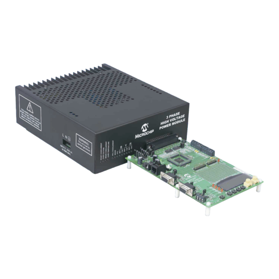
HIGH VOLTAGE POWER MODULE Chapter 1. Set Up and Operation INTRODUCTION The Microchip dsPICDEM MC1H 3-Phase High Voltage Power Module is intended to aid the user in the rapid evaluation and development of a wide variety of motor control ®... - Page 12 MC1H 3-Phase High Voltage Power Module FIGURE 1-2: MC1H 3-PHASE HIGH VOLTAGE POWER MODULE BLOCK DIAGRAM From To Gate Control Drive 1-8 Board Control Board DS70096A-page 6 © 2003 Microchip Technology Inc.
-
Page 13: Using The Motor Control 3-Phase High Power Module
The power connections are shown in Table 1-1 and Figure 1-3: TABLE 1-1: POWER CONNECTIONS Connection Number Input Output Ground Ground Neutral Red Phase Live (Fused) Yellow Phase — Blue Phase — -DC Bus — External Brake Resistor — +DC Bus © 2003 Microchip Technology Inc. DS70096A-page 7... - Page 14 DC-DC converter that is connected to the digital +5V supply input on the 37-pin connector. In this way, the power module may be used at any input voltage up to the maximum. This arrangement is shown in Figure 1-4. DS70096A-page 8 © 2003 Microchip Technology Inc.
- Page 15 No electrical isolation is provided on the control board for these signals and so the transducers must be isolated. Consult the development board documentation for details of signal interfacing and how to connect in-circuit emulators and debugging equipment. © 2003 Microchip Technology Inc. DS70096A-page 9...
- Page 16 16 kHz carrier frequency be used. This offers lower loss while still being inaudible. It also has the advantage that the dead time insertion will cause less distortion of the output voltage. DS70096A-page 10 © 2003 Microchip Technology Inc.
- Page 17 If necessary, the user should periodically apply a refresh pulse to the low side switch in a similar manner to that described for priming above. © 2003 Microchip Technology Inc. DS70096A-page 11...
- Page 18 * If a large rate of change of current occurs due to the use of a load with low inductance, the voltage across the self-inductance of the shunts will cause an additional shunt voltage that will add to the shunt feedback signals. DS70096A-page 12 © 2003 Microchip Technology Inc.
- Page 19 A stall trip time of 2 seconds is suggested. © 2003 Microchip Technology Inc. DS70096A-page 13...
-
Page 20: Current And Power Limitations
The complementary diode of the inverter phase will also conduct for approximately 50% thus spreading the conduction loss between two different power device packages. This in turn leads to a substantial reduction in device temperature. DS70096A-page 14 © 2003 Microchip Technology Inc. - Page 21 AC input voltage and the DC bus voltage (i.e., the larger the average boost ratio). This is because the average switch duty cycle increases the larger the boost ratio and therefore the switch conduction loss increases. Furthermore, the switching loss also increases slightly with boost ratio. © 2003 Microchip Technology Inc. DS70096A-page 15...
- Page 22 PFC. Given the development nature of the system, the capacitance was oversized to assist those users wishing to use the system without the PFC or at lower voltages. Figure 1-6 gives the peak-peak DC bus voltage ripple for three different conditions. DS70096A-page 16 © 2003 Microchip Technology Inc.
-
Page 23: Detailed Description Of Operation
• BR1 – A single-phase bridge rectifier to convert the incoming AC into DC suitable for input to the power conditioning stage. • V1 – A metal oxide varistor located across the incoming supply lines to suppress high energy transients. © 2003 Microchip Technology Inc. DS70096A-page 17... - Page 24 2A of peak gate drive current to switch Q1 and Q2 rapidly and therefore achieve low switching loss. It also has a small footprint allowing it to be located physically close to the transistors allowing a low inductance gate circuit layout. DS70096A-page 18 © 2003 Microchip Technology Inc.
- Page 25 The under-voltage lockout is automatically reset by a rising edge of a firing command once a valid voltage is present. See www.irf.com for a full data sheet. © 2003 Microchip Technology Inc. DS70096A-page 19...
- Page 26 Apart from acoustic noise reasons, there is no reason to modulate the device at high frequency. As the tab of the device is not isolated, a thermally conductive insulator is used. DS70096A-page 20 © 2003 Microchip Technology Inc.
- Page 27 ±4.8A and a gain of 2.4A/V. Note that a third device is not required, as the sum of the output line currents must always be zero due to symmetry. The one exception to this is during a ground FAULT condition that is detected elsewhere. © 2003 Microchip Technology Inc. DS70096A-page 21...
- Page 28 Note that in applications requiring less gain and/or slower speed of response, the MCP602/604 family offers a good alternative with even lower power supply consumption. DS70096A-page 22 © 2003 Microchip Technology Inc.
- Page 29 It does not matter whether the current actually flows in the switch or the anti-parallel diode. The result depends only on the magnitude and direction of the output currents, see Table 1-5. © 2003 Microchip Technology Inc. DS70096A-page 23...
- Page 30 The first two of these signals are available as isolated signals, whereas the inverter output voltages are only available when the system is used in the non-isolated manner (see Section 1.2.6.3 “Non-isolated Feedback” and Section 1.5.3.4 “Accessing the Additional (non-isolated) Feedback Signals”). DS70096A-page 24 © 2003 Microchip Technology Inc.
- Page 31 Output Voltage Feedback and Sensorless Detection”). • C57 – This acts to filter out any noise spikes on the DC bus voltage sensing circuit. • D40, D42 – Clamping diodes to protect the PIC12C671 inputs. © 2003 Microchip Technology Inc. DS70096A-page 25...
- Page 32 • R143, R147 – These provide a small amount of hysteresis to prevent oscillation of R_CROSSING. • R142 – The pull-up resistor for the open-collector output of the comparator. DS70096A-page 26 © 2003 Microchip Technology Inc.
- Page 33 • U5 – A 5V linear regulator for the live control circuit supplies. • D4 – A 1A diode to protect U5 against reverse bias during power-down. • R61 – A 0Ω resistor linking the low voltage power supply star point to the -DC bus. © 2003 Microchip Technology Inc. DS70096A-page 27...
- Page 34 The SET dominance is important to ensure correct fault action even if the RESET input is active. • D5, R202 – An LED and its associated current limiting resistor for the visual indication of the FAULT. DS70096A-page 28 © 2003 Microchip Technology Inc.
- Page 35 The one difference is that the input signals to the comparator are divided down in order to stay within the input voltage limitations of the comparators when running from +5V. © 2003 Microchip Technology Inc. DS70096A-page 29...
-
Page 36: Modifying The Board
LK4. LK4 is located directly under the “Danger High Voltage” label on the PCB as shown in Section 9. Table 1-6 shows the settings: TABLE 1-6: SHUNT FEEDBACK POLARITY SELECTION LK 4 Setting Feedback Range Bipolar Unipolar DS70096A-page 30 © 2003 Microchip Technology Inc. - Page 37 The scaling and corresponding trip levels for U2 are shown in Table 1-9. TABLE 1-9: HALL EFFECT BUS CURRENT TRANSDUCER SCALING SELECTION LK 3 Closed LK2 Closed LK1 Closed Scaling (A / V) ±5.9 ±8.9 ±17.8 Trip Level (A) © 2003 Microchip Technology Inc. DS70096A-page 31...
- Page 38 PCB is 4 mm. • Once the modification is complete, install the lid ensuring all the screws are replaced. DS70096A-page 32 © 2003 Microchip Technology Inc.
- Page 39 • Once the modification is complete, install the lid ensuring all the screws are replaced. • Note that the maximum continuous limit on input current increases to 6A (RMS) limited by the loss in the PFC inductor. © 2003 Microchip Technology Inc. DS70096A-page 33...
- Page 40 The digital 0V of the control card is permanently connected to the enclosure chassis and is therefore also referenced to ground. • Once the modification is complete, install the lid ensuring all the screws are replaced. DS70096A-page 34 © 2003 Microchip Technology Inc.
- Page 41 No guarantee or liability can be accepted for any modifications that the user makes to the system. If the user removes the PCB from the enclosure chassis, they should ensure that the power device clamping force and the insulation is unaltered when the PCB is re-installed. © 2003 Microchip Technology Inc. DS70096A-page 35...
-
Page 42: Test Points
TP 17 Live +5V power supply TP 18 ISOLATED High reference used for FAULT trips ISO_HIGH_REF TP 19 ISOLATED Low reference used for FAULT trips ISO_LOW_REF TP 20 LIVE Star Reference Point for Low Voltage PSUs — DS70096A-page 36 © 2003 Microchip Technology Inc. -
Page 43: User Signal Connector Pinout (37-Pin, D-Type)
Output Fault Reset Command ISO_RESET Input Not Used — — — Red Phase Hall Current Sensor Feedback R_HALL Output Digital GND from control PCB ISO_GND Input Digital +5V from control PCB(±2%) ISO_+5V Input © 2003 Microchip Technology Inc. DS70096A-page 37... - Page 44 MC1H 3-Phase High Voltage Power Module NOTES: DS70096A-page 38 © 2003 Microchip Technology Inc.
-
Page 45: Appendix A: Circuit Diagrams
MC1H 3-PHASE HIGH VOLTAGE POWER MODULE Appendix A. Circuit Diagrams CIRCUIT DIAGRAMS © 2003 Microchip Technology Inc. DS70096A-page 39... - Page 46 MC1H 3-Phase High Voltage Power Module DS70096A-page 40 © 2003 Microchip Technology Inc.
- Page 47 Appendix © 2003 Microchip Technology Inc. DS70096A-page 41...
- Page 48 MC1H 3-Phase High Voltage Power Module DS70096A-page 42 © 2003 Microchip Technology Inc.
- Page 49 Appendix © 2003 Microchip Technology Inc. DS70096A-page 43...
- Page 50 MC1H 3-Phase High Voltage Power Module DS70096A-page 44 © 2003 Microchip Technology Inc.
- Page 51 Appendix © 2003 Microchip Technology Inc. DS70096A-page 45...
- Page 52 MC1H 3-Phase High Voltage Power Module DS70096A-page 46 © 2003 Microchip Technology Inc.
-
Page 53: Appendix B: Source Code
VDC Bus |VAC| No Data Activity 1 Cycle of Data = 128 µs Note: The data transmitted via the SPI interface is inverted by the opto-isolators. The user software should invert the received data. © 2003 Microchip Technology Inc. DS70096A-page 47... - Page 54 0X02 ;AD0,AD1 and AD2 are analog channels movwf ADCON1 ;with VDD and VSS references call 0x03ff ;factory programmed data to trim movwf OSCCAL ;internal oscillator clrf STATUS ;select bank0 FOR REST OF CODE DS70096A-page 48 © 2003 Microchip Technology Inc.
- Page 55 ;send bit 7 GPIO,SCK btfsc BYTE_TO_SEND,7 GPIO,SDO GPIO,SCK GPIO,SDO ;send bit 6 GPIO,SCK btfsc BYTE_TO_SEND,6 GPIO,SDO GPIO,SCK GPIO,SDO ;send bit 5 GPIO,SCK btfsc BYTE_TO_SEND,5 GPIO,SDO GPIO,SCK GPIO,SDO ;send bit 4 GPIO,SCK btfsc BYTE_TO_SEND,4 GPIO,SDO GPIO,SCK © 2003 Microchip Technology Inc. DS70096A-page 49...
- Page 56 GPIO,SDO GPIO,SCK ;set up ADC to begin sampling channel 0 movlw 0x41 ;Fosc/8, A/D enabled channel 0 selected movwf ADCON0 ;begin sampling ch0 BUS_SENSE GPIO,SDO ;send bit 6 GPIO,SCK btfsc BYTE_TO_SEND,6 GPIO,SDO GPIO,SCK DS70096A-page 50 © 2003 Microchip Technology Inc.
- Page 57 GPIO,SDO ;send bit 0 GPIO,SCK btfsc BYTE_TO_SEND,0 GPIO,SDO GPIO,SCK ;while ADC is still converting Channel 0, send control word 0xF9 GPIO,SCK ;send bit7 GPIO,SDO GPIO,SCK GPIO,SCK ;send bit6 GPIO,SCK GPIO,SCK ;send bit5 GPIO,SCK © 2003 Microchip Technology Inc. DS70096A-page 51...
- Page 58 GPIO,SCK ;send bit3 GPIO,SCK GPIO,SCK ;send bit2 GPIO,SDO GPIO,SCK GPIO,SCK ;send bit1 GPIO,SCK GPIO,SCK ;send bit0 GPIO,SDO GPIO,SCK ;conversion of channel 0 now complete movf ADRES,W movwf BYTE_TO_SEND goto Main ;Do it again DS70096A-page 52 © 2003 Microchip Technology Inc.
- Page 59 Appendix NOTES: © 2003 Microchip Technology Inc. DS70096A-page 53...
-
Page 60: Worldwide Sales And Service
ASIA/PACIFIC Japan Microchip Technology Japan K.K. Corporate Office Australia Benex S-1 6F 2355 West Chandler Blvd. Microchip Technology Australia Pty Ltd 3-18-20, Shinyokohama Chandler, AZ 85224-6199 Marketing Support Division Kohoku-Ku, Yokohama-shi Tel: 480-792-7200 Fax: 480-792-7277 Suite 22, 41 Rawson Street... - Page 61 Mouser Electronics Authorized Distributor Click to View Pricing, Inventory, Delivery & Lifecycle Information: Microchip DM300021...
Need help?
Do you have a question about the dsPICDEM MC1H and is the answer not in the manual?
Questions and answers