Advertisement
Quick Links
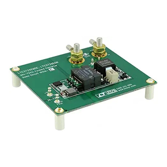
QUICK START GUIDE FOR DEMONSTRATION CIRCUIT 888A-B
DESCRIPTION
Demonstration circuit 888A-B is a high power iso-
lated synchronous forward converter featuring the
LTC3725 and LTC3706. When powered from a 36-
72V input, a single DC888A-B provides an isolated
5V at 40A in a quarter-brick footprint. If higher out-
put current is required, multiple DC888A boards may
be stacked together using on-board connectors for a
complete PolyPhase current sharing solution. The
converter operates at 250kHz and achieves efficiency
up to 93.5% with synchronous output rectifiers.
Secondary-side control eliminates complex optocou-
Table 1. Performance Summary (T
PARAMETER
Minimum Input Voltage
Maximum Input Voltage
Output Voltage V
OUT
Maximum Output Current
Typical Output Ripple V
OUT
Output Regulation
Load Transient Response
Nominal Switching Frequency
Efficiency
Isolation
Size
OPERATING PRINCIPLES – SINGLE PHASE
The LTC3706 secondary side controller is used on the
secondary and the LTC3725 smart driver with self-
starting capability is used on the primary. When an
input voltage is applied, the LTC3725 (U1 in Figure
15), which is powered through R29 and Q28, begins
a controlled soft-start of the output voltage by switch-
ing MOSFETs Q9 and Q11. As the output voltage be-
gins to rise, the LTC3706 secondary controller is
quickly powered up via D24, Q29, C67, and Q27. The
36V-72VIN, ISOLATED SYNCHRONOUS FORWARD
= 25°C)
A
CONDITION
V
= 36V to 72V, I
IN
200LFM
V
= 48V, I
= 40A, 250kHz
IN
OUT
Over All Input Voltages and Output Currents
Peak Deviation with 20A to 40A Load Step (10A/us)
Settling Time
V
= 36V, I
= 28A
IN
OUT
BASIC
Component Area x Top x Bottom Component Height
pler feedback, providing fast transient response with
a minimum amount of output capacitance. Additional
DC888A versions include DC888A-A (3.3V at 50A)
and DC888A-C (12V at 20A). The simple architecture
can be easily modified to meet different input and
output voltage requirements.
Design files for this circuit board are available.
Call the LTC factory.
, LTC and LT are registered trademarks of Linear Technology Corporation.
= 0A to 40A
OUT
LTC3706 then assumes control of the output voltage
by sending encoded PWM gate pulses to the
LTC3725 primary driver via signal transformer, T2.
The LTC3725 then operates as a simple driver receiv-
ing both input signals and bias power through T2.
The transition from primary to secondary control oc-
curs seamlessly at a fraction of the output voltage.
From that point on, operation and design simplifies to
that of a simple buck converter. The LTC3706 regu-
LTC3725/LTC3706
VALUE
36V
72V
5V
40A
< 60mV
P–P
±1% (Reference)
±250mV
•50us
250kHz
93.5% Typical
1500VDC
2.3" x 1.45" x 0.4" x 0.075"
1
Advertisement

Related Manuals for Linear Technology LTC3725


Summary of Contents for Linear Technology LTC3725
- Page 1 PolyPhase current sharing solution. The Call the LTC factory. converter operates at 250kHz and achieves efficiency , LTC and LT are registered trademarks of Linear Technology Corporation. up to 93.5% with synchronous output rectifiers. Secondary-side control eliminates complex optocou- Table 1.
-
Page 2: Quick Start Procedure
OPERATING PRINCIPLES – POLYPHASE The LTC3725 and LTC3706 allow the user to develop FS/SYNC pin of the slave (Figures 19 and 20). The modular power supply “building blocks” that can be relative clock phase of each stage is determined by added as power/current requirements increase. - Page 3 Make sure that the input voltage •72V. NOTE: bility. This may require a damping impedance. (See Linear Technology Application Note AN19 for a Check for the proper output voltage of 5V. discussion of input filter stability.) A source with a Turn off the power at the input.
- Page 4 QUICK START GUIDE FOR DEMONSTRATION CIRCUIT 888A-B 36V-72VIN, ISOLATED SYNCHRONOUS FORWARD Figure 1. Proper Measurement Equipment Setup Figure 2. Measuring Input or Output Ripple...
-
Page 5: Measured Data
QUICK START GUIDE FOR DEMONSTRATION CIRCUIT 888A-B 36V-72VIN, ISOLATED SYNCHRONOUS FORWARD MEASURED DATA Figures 3 through 14 are measured data for a typical DC888A-B. Figures 15 through 23 consist of schematics, bill of materials, and a picture. Figure 3. Efficiency Figure 4. - Page 6 QUICK START GUIDE FOR DEMONSTRATION CIRCUIT 888A-B 36V-72VIN, ISOLATED SYNCHRONOUS FORWARD Figure 5. Load Transient Response (48Vin, 20A to 40A to 20A at 10A/us, Single Phase) Figure 6. Loop Response (48Vin, 4A & 40A, Single Phase)
- Page 7 QUICK START GUIDE FOR DEMONSTRATION CIRCUIT 888A-B 36V-72VIN, ISOLATED SYNCHRONOUS FORWARD Figure 7. Turn-on (48Vin, 40A, Single Phase) Figure 8. Turn-on (48Vin, 80A, PolyPhase)
- Page 8 QUICK START GUIDE FOR DEMONSTRATION CIRCUIT 888A-B 36V-72VIN, ISOLATED SYNCHRONOUS FORWARD Figure 9. Transient Sharing of Inductor Current (48Vin, 30A to 60A, PolyPhase) Figure 10. Transient Sharing of Inductor Current (48Vin, 60A to 30A, PolyPhase)
- Page 9 QUICK START GUIDE FOR DEMONSTRATION CIRCUIT 888A-B 36V-72VIN, ISOLATED SYNCHRONOUS FORWARD Figure 11. Temp Data (48Vin, 40A, 200LFM airflow – top) Figure 12. Temp Data (48Vin, 40A, 200LFM airflow – bottom)
- Page 10 QUICK START GUIDE FOR DEMONSTRATION CIRCUIT 888A-B 36V-72VIN, ISOLATED SYNCHRONOUS FORWARD Figure 13. Temp Data (48Vin, 36A, 0LFM airflow – top) Figure 14. Temp Data (48Vin, 36A, 0LFM airflow – bottom)
- Page 11 QUICK START GUIDE FOR DEMONSTRATION CIRCUIT 888A-B 36V-72VIN, ISOLATED SYNCHRONOUS FORWARD Figure 15. Single Phase Schematic...
- Page 12 QUICK START GUIDE FOR DEMONSTRATION CIRCUIT 888A-B 36V-72VIN, ISOLATED SYNCHRONOUS FORWARD Figure 16. Full Single Phase Schematic...
- Page 13 QUICK START GUIDE FOR DEMONSTRATION CIRCUIT 888A-B 36V-72VIN, ISOLATED SYNCHRONOUS FORWARD Reference Part Description Manufacturer / Part # REQUIRED CIRCUIT COMPONENTS C3,C4,C5 CAP., X7R, 2.2uF, 100V, 20%, 1210 Murata, GRM32ER72A225K C24,C71 CAP., X7R, 1.0uF, 16V 10%, 0805 TAIYO YUDEN, EMK212BJ105KG C27, CAP., C0G, 100pF, 50V, 10%, 0603 AVX, 06035A101KAT2A...
- Page 14 QUICK START GUIDE FOR DEMONSTRATION CIRCUIT 888A-B 36V-72VIN, ISOLATED SYNCHRONOUS FORWARD Figure 17. Bill of Materials (Single Phase) RES., CHIP, 1.0K, 1/16W, 5%, 0805 VISHAY, CRCW08051K00JNEA RES., CHIP, 100K, 1/8W, 5%, 0805 VISHAY, CRCW0805100KJNEA RES., CHIP, 604, 1/16W, 1%, 0603 VISHAY, CRCW0603604RFKEA RES., CHIP, 12, 1/16W, 5%, 0603 VISHAY, CRCW060312R0JNEA...
- Page 15 QUICK START GUIDE FOR DEMONSTRATION CIRCUIT 888A-B 36V-72VIN, ISOLATED SYNCHRONOUS FORWARD Single Phase PolyPhase 10nF 4.7nF 3.3nF 15nF 10nF 4.7nF 0Ω 0Ω 0Ω 10nF 4.7nF 3.3nF 15nF 10nF 4.7nF 3.3nF open 4.42kΩ open 604Ω open 0Ω 0Ω 0Ω 100kΩ open 0Ω...
- Page 16 QUICK START GUIDE FOR DEMONSTRATION CIRCUIT 888A-B 36V-72VIN, ISOLATED SYNCHRONOUS FORWARD Figure 19. PolyPhase Master Schematic...
- Page 17 QUICK START GUIDE FOR DEMONSTRATION CIRCUIT 888A-B 36V-72VIN, ISOLATED SYNCHRONOUS FORWARD Figure 20. PolyPhase Slave Schematic...
- Page 18 QUICK START GUIDE FOR DEMONSTRATION CIRCUIT 888A-B 36V-72VIN, ISOLATED SYNCHRONOUS FORWARD Figure 21. Full PolyPhase Master Schematic...
- Page 19 QUICK START GUIDE FOR DEMONSTRATION CIRCUIT 888A-B 36V-72VIN, ISOLATED SYNCHRONOUS FORWARD Figure 22. Full PolyPhase Slave Schematic...
- Page 20 QUICK START GUIDE FOR DEMONSTRATION CIRCUIT 888A-B 36V-72VIN, ISOLATED SYNCHRONOUS FORWARD Figure 23. Picture of two DC888A’s configured for PolyPhase...
Need help?
Do you have a question about the LTC3725 and is the answer not in the manual?
Questions and answers