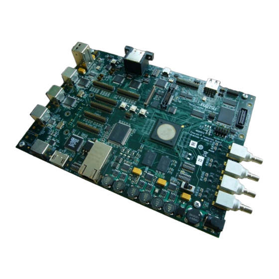
Summary of Contents for Fujitsu MB86R12
- Page 1 MB86R12 Application Note DDR3 Interface PCB Design Guideline November, 2011 The 1.0 edition FUJITSU SEMICONDUCTOR CONFIDENTIAL...
- Page 3 When you develop equipment incorporating the device based on such information, you must assume any responsibility arising out of such use of the information. FUJITSU SEMICONDUCTOR assumes no liability for any damages whatsoever arising out of the use of the information.
- Page 4 MB86R12 Application Note DDR3 Interface PCB Design Guideline Revision History Date Ver. Contents 2011/11/29 Newly issued FUJITSU SEMICONDUCTOR CONFIDENTIAL...
-
Page 5: Table Of Contents
MB86R12 Application Note DDR3 Interface PCB Design Guideline Contents 1. Floor plan ......................1 2. PCB laminating ....................2 3. DDR3_SDRAM specifications ................3 4. Signal design restrictions (DDR3 interface part) ..........4 4.1. Definition of signal line group ........................ 4 4.2. -
Page 7: Floor Plan
MB86R12 Application Note DDR3 Interface PCB Design Guideline Floor plan Figure 1-1 shows the reference example of the floor plan of MB86R12 and connected DDR3 SDRAM devices. SDRAM MB86R12 27mm SDRAM 10mm 15.5mm 27mm 32mm Figure 1-1 Reference example of the floor plan of MB86R12 and DDR3 SDRAM devices... -
Page 8: Pcb Laminating
MB86R12 Application Note DDR3 Interface PCB Design Guideline PCB laminating This chapter shows the recommended laminating conditions of the PCB. Insulator thickness Conductor Classification thickness 40μm Resist thickness L1 43μm SIG. (copper foil: 18mm, plating: 25mm) 100μm L2 35μm Power 150μm... -
Page 9: Ddr3_Sdram Specifications
DDR3 Interface PCB Design Guideline DDR3_SDRAM specifications This chapter shows DDR3_SDRAM that can be used for the DDR3 interface with MB86R12. If an alternative device fulfills the same requirements, it can also used. Please note however, that if you use an alternative device, there may be differences concerning I/O quality which may require your attention. -
Page 10: Signal Design Restrictions (Ddr3 Interface Part)
In order to make the requirements for wiring configurations described further on in this document easier to understand, the DDR3 interface signals are classified into the groups listed below. Table 4-1 DDR3 interface signal grouping Wiring preferential Group name Pin name of MB86R12 order MCK_Group MCK, MXCK MDQS0_Group MDQS0, MXDQS0... -
Page 11: General Wiring Restrictions
MB86R12 Application Note DDR3 Interface PCB Design Guideline 4.2. General wiring restrictions This section describes the general wiring restrictions. • It is recommended that signal wiring be designed to have the following characteristic impedance. Single impedance: 50Ω±10% Differential impedance: 100Ω±10% •... -
Page 12: Terminal Resistance/Damping Resistance/Wire Length
MB86R12 Application Note DDR3 Interface PCB Design Guideline 4.4. Terminal resistance/Damping resistance/Wire length Table 4-2 shows the recommended resistance value and wire length for each group. The wiring topology diagram relevant to this section is shown in "4.7. Wiring topology". -
Page 13: Wiring Gap/Crosstalk
MB86R12 Application Note DDR3 Interface PCB Design Guideline 4.5. Wiring gap/Crosstalk Please keep to the wiring configurations shown below in order to avoid malfunctions and deteriorated signal integrity due to crosstalk. (1) The recommended gap for wiring within MDQx_Group and MCMD_Group groups should be over 300µm. -
Page 14: Zq/Odt Setting
DDR3 Interface PCB Design Guideline 4.6. ZQ/ODT setting Table 4-3 shows the ZQ setting conditions. Table 4-3 ZQ setting conditions Group name Output impedance of MB86R12 I/O (RON) ZQ setting of MB86R12 MCK_Group 40Ω MDQSx_Group 48Ω Perform the ZQ calibration, and set it MDQx_Group 48Ω... -
Page 15: Wiring Topology
MB86R12 Application Note DDR3 Interface PCB Design Guideline 4.7. Wiring topology This section illustrates the recommended wiring topology of each group. 4.7.1. Wiring topology diagram of MCK_Group DDR3_ MB86R12 SDRAM For DQ[15:0] L1 (24.8mm 25.3mm) RON: 40[Ω] (15.5mm 15.9mm) Wire length of each CLK signal Signal name Length of wiring "L1 + L2"... -
Page 16: Wiring Topology Diagram Of Mdqsx_Group
MB86R12 Application Note DDR3 Interface PCB Design Guideline 4.7.2. Wiring topology diagram of MDQSx_Group DDR3_ MB86R12 SDRAM Wire length of each DQS signal Driver strength: 34[Ω] RON: 48[Ω] Signal name Length of wiring "L1" [mm] ODT: 60[Ω] ODT: 40[Ω] MDQS0/MXDQS0 30.9±3 (Differential and equal-length) -
Page 17: Wiring Topology Diagram Of Mdqx_Group
MB86R12 Application Note DDR3 Interface PCB Design Guideline 4.7.3. Wiring topology diagram of MDQx_Group DDR3_ MB86R12 SDRAM Driver strength: 34[Ω] RON: 48[Ω] ODT: 60[Ω] ODT: 40[Ω] - In wiring, the L3/L6 layer is assumption. - Wire length doesn't contain the length of the via. -
Page 18: Wiring Topology Diagram Of Mcntl_Group/Mcmd_Group
0.6mm or less DDR3_ MB86R12 SDRAM For DQ[15:0] L1 (31.0mm 44.7mm) RON: 60[Ω] (17.1mm 17.4mm) Wire length from MB86R12 to DDR3_ SDRAM at the farthest position 0.6mm or less SDRAM (48.7mm 62.7mm) For DQ[31:16] VTT=DDRVDE/2 L1/L8 layer - In wiring, the L3/L6 layer is assumption. -
Page 19: Power System Design Restrictions
• If capacity is a value close to 0.1µF (0.22µF etc. for instance), the bypass capacitor can be used. • Place the 0.1µF capacitor as close as possible to the power/GND pins of MB86R12 (refer to "5.2. Pull-out wiring condition"). -
Page 20: Pull-Out Wiring Condition
If it doesn't meet these conditions, widen the wire width as much as possible, and shorten the wire length. Note 1) There is no problem even if the Chip on Via method without the pull-out wiring is used. L1 layer MB86R11 PAD L1 layer MB86R12 PAD Power [Pull-out wiring conditions] Wire width (W): over 0.3mm...


Need help?
Do you have a question about the MB86R12 and is the answer not in the manual?
Questions and answers