National Instruments PXIe-5665 Calibration Manual
Calibration procedure
3.6 ghz and 14 ghz rf vector signal analyzer
Hide thumbs
Also See for PXIe-5665:
- Getting started manual (10 pages) ,
- Getting started manual (33 pages) ,
- Getting started manual (9 pages)
Table of Contents
Advertisement
Quick Links
CALIBRATION PROCEDURE
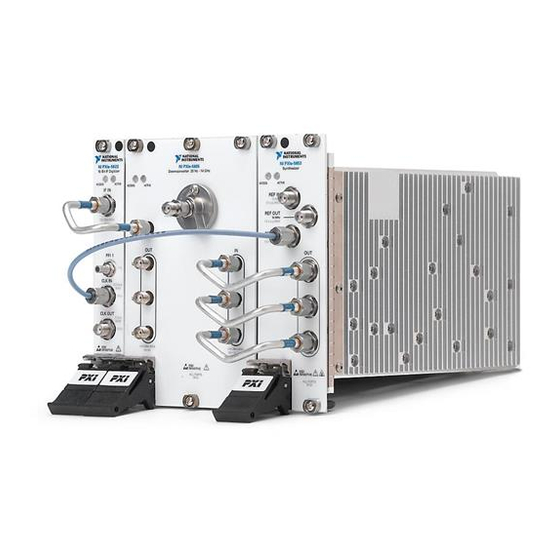
PXIe-5665
3.6 GHz and 14 GHz RF Vector Signal Analyzer
This document contains the verification procedures for the National Instruments PXIe-5665
RF vector signal analyzer (VSA). Refer to
calibration solutions.
When not otherwise specified, the procedures in this document refer to both the PXIe-5665
3.6 GHz VSA and the PXIe-5665 14 GHz VSA products. In places where the procedures differ
between the two products, the appropriate device settings are specified.
PXIe-5665 tuned frequencies greater than 3.6 GHz and procedures with the
Note
preselector enabled for frequencies greater than 3.6 GHz apply only to the PXIe-5665
14 GHz VSA.
NI warrants the PXIe-5665 to meet its published specifications if the individual modules are
calibrated and operating within specifications. For more information about RF system
calibration, visit
ni.com/manuals
Contents
Software.................................................................................................................................... 2
Documentation.......................................................................................................................... 2
Test Equipment......................................................................................................................... 3
Test Conditions......................................................................................................................... 10
System Options......................................................................................................................... 11
Initial Setup............................................................................................................................... 11
Characterizing the Test System ................................................................................................ 11
Zeroing and Calibrating the Power Sensor....................................................................... 11
Characterizing Power Splitter Reference Output ............................................................. 11
Characterizing Power Splitter Difference......................................................................... 12
Characterizing RF Source Power (Direct)........................................................................ 13
Characterizing RF Source Power (with Lowpass Filter).................................................. 15
Characterizing RF Source Power (Combined) for Frequencies ≤700 MHz..................... 17
Characterizing RF Source Power (Combined) for Frequencies >700 MHz..................... 19
Characterizing RF Source Power (Through Splitter) ....................................................... 21
Characterizing RF Source Power (with Splitter and Attenuator) ..................................... 23
Characterizing Spectrum Analyzer Response .................................................................. 25
As-Found and As-Left Limits................................................................................................... 27
Verification ............................................................................................................................... 27
Verifying Reference Accuracy ......................................................................................... 27
Verifying Phase Noise ...................................................................................................... 27
ni.com/calibration
and search for
Letter of Conformance
for more information about
.
Advertisement
Table of Contents

Related Manuals for National Instruments PXIe-5665


Summary of Contents for National Instruments PXIe-5665
-
Page 1: Table Of Contents
When not otherwise specified, the procedures in this document refer to both the PXIe-5665 3.6 GHz VSA and the PXIe-5665 14 GHz VSA products. In places where the procedures differ between the two products, the appropriate device settings are specified. -
Page 2: Software
Appendix A: Anti-Distortion Test Fixture................83 Appendix B: Power Sensor Calibration Factor Uncertainty............. 84 Worldwide Support and Services ..................... 85 Software Calibrating the PXIe-5665 requires you to install the following software on the calibration system: • NI-RFSA 2.5 or later •... -
Page 3: Test Equipment
Test Equipment Table 1 lists the equipment NI recommends for the performance verification procedures. If the recommended equipment is not available, select a substitute using the minimum requirements listed in the table. PXIe-5665 Calibration Procedure | © National Instruments | 3... - Page 4 Table 1. Recommended Equipment for PXIe-5665 Calibration Equipment Recommended Models Where Used Minimum Requirements Power meter Anritsu ML2438A Verifying frequency response, Display resolution: ≤0.01 dB Verifying absolute amplitude accuracy, Settling: ±0.1% Verifying LO output power Instrumentation accuracy: <±0.5% Noise, zero set, and drift: ≤±0.5% full-scale (lowest range) Reference power uncertainty: ≤±0.9%...
- Page 5 Table 1. Recommended Equipment for PXIe-5665 Calibration (Continued) Equipment Recommended Models Where Used Minimum Requirements Signal generator Anritsu MG3692C Verifying third-order intermodulation Frequency range: 8 MHz to 16 GHz (RF source 1) distortion, Leveled power: -115 dBm to 18 dBm...
- Page 6 Table 1. Recommended Equipment for PXIe-5665 Calibration (Continued) Equipment Recommended Models Where Used Minimum Requirements Spectrum analyzer Rohde & Schwarz FSUP26 Verifying frequency response, Frequency range: 10 MHz to 18 GHz Verifying phase noise, Noise floor: <-152 dBm/Hz Options B60 and B61...
- Page 7 Table 1. Recommended Equipment for PXIe-5665 Calibration (Continued) Equipment Recommended Models Where Used Minimum Requirements SMA (m)-to- MegaPhase — Frequency range: DC to 18 GHz SMA (m) cables G916-SISI-36 Insertion loss: ≤2 dB at 18 GHz (36 in.) (3x) Impedance: 50 Ω...
- Page 8 Table 1. Recommended Equipment for PXIe-5665 Calibration (Continued) Equipment Recommended Models Where Used Minimum Requirements SMA (m)-to- Huber+Suhner — Frequency range: DC to 18 GHz SMA (f) 20 dB 6620_SMA-50-1/199N Attenuation: 20 dB (nominal) attenuator Power rating: 2 W average Impedance: 50 Ω...
- Page 9 Table 1. Recommended Equipment for PXIe-5665 Calibration (Continued) Equipment Recommended Models Where Used Minimum Requirements Frequency reference Symmetricom 8040 — Frequency: 10 MHz source rubidium frequency standard Frequency accuracy: ±1 × 10 Test Conditions Torque wrench — — Refer to for torque wrench specifications.
-
Page 10: Test Conditions
Test Conditions The following setup and environmental conditions are required to ensure the PXIe-5665 meets published specifications. • Keep cabling as short as possible. Long cables and wires act as antennae, picking up extra noise that can affect measurements. •... -
Page 11: System Options
• 25 MHz instantaneous bandwidth: Verification procedures include any changes necessary to accommodate this option. There are no changes to the PXIe-5665 specifications for this digitizer option. Initial Setup Refer to the NI PXIe-5665 RF Vector Signal Analyzer Getting Started Guide for information about how to install the software and hardware and how to configure the device in Measurement &... -
Page 12: Characterizing Power Splitter Difference
Set the power sensors calibration factor for the measurement frequency at 4 GHz. Calculate the Power Splitter at 4 GHz Correction Factor using the following formula: Power Splitter at 4 GHz Correction Factor = Corrected Power Sensor B Power - Corrected Power Sensor A Power 12 | ni.com | PXIe-5665 Calibration Procedure... -
Page 13: Characterizing Rf Source Power (Direct)
SMA (m)-to-SMA (m) Cable Power Sensor B Set the RF source 2 frequency according to the first row in Table 2 or Table 3 as appropriate. Table 2. PXIe-5665 3.6 GHz VSA RF Source 2 Characterization Frequencies Start Frequency Stop Frequency Step Size 100.033325 MHz... - Page 14 Table 2. PXIe-5665 3.6 GHz VSA RF Source 2 Characterization Frequencies (Continued) Start Frequency Stop Frequency Step Size 25.033325 MHz 1.625033325 GHz 100 MHz 1.724966675 GHz 3.224966675 GHz 100 MHz 3.3875 GHz — — 987.5 MHz — — Table 3. PXIe-5665 14GHz VSA RF Source 2 Characterization Frequencies...
-
Page 15: Characterizing Rf Source Power (With Lowpass Filter)
RF Source 2 3.5 mm (f)-to-3.5 mm (f) Adaptor SMA (m)-to-SMA (m) Cable Power Sensor B SMA (m)-to-SMA (m) Cable Power Meter Anti-Distortion Test Fixture Disable the RF source 1 output. PXIe-5665 Calibration Procedure | © National Instruments | 15... - Page 16 Table 4. The final RF source 2 power setting is the RF Source Power LPF for that frequency. Repeat steps 3 to 6 for all the frequencies and powers in Table 4. 16 | ni.com | PXIe-5665 Calibration Procedure...
-
Page 17: Characterizing Rf Source Power (Combined) For Frequencies ≤700 Mhz
3.5 mm (f)-to-3.5 mm (f) Adaptor SMA (m)-to-SMA (m) Cable Power Sensor B SMA (m)-to-SMA (m) Cable Power Meter Anti-Distortion Test Fixture Set the anti-distortion test fixture to the ≤700 MHz combiner path. PXIe-5665 Calibration Procedure | © National Instruments | 17... - Page 18 Table 6. The RF source 1 power is the RF Source 1 Programmed Power. 10. Repeat steps 3 to 9 for all remaining frequency and power values in Table 6. 18 | ni.com | PXIe-5665 Calibration Procedure...
-
Page 19: Characterizing Rf Source Power (Combined) For Frequencies >700 Mhz
3.5 mm (f)-to-3.5 mm (f) Adaptor SMA (m)-to-SMA (m) cable Power Sensor B SMA (m)-to-SMA (m) cable Power Meter Anti-Distortion Test Fixture Set the anti-distortion test fixture to the >700 MHz combiner path. PXIe-5665 Calibration Procedure | © National Instruments | 19... - Page 20 Set the RF source 1 and RF source 2 frequency and power values according to the first row in Table 7. Table 7. PXIe-5665 RF Source Power (Combined) Test Settings (Frequencies >700 MHz) RF Source 1 RF Source 2 Start...
-
Page 21: Characterizing Rf Source Power (Through Splitter)
Connect the RF source 2 output to the power splitter input through the SMA (m)-to- SMA (m) cable. Connect a 50 Ω termination load to the reference output of the power splitter. PXIe-5665 Calibration Procedure | © National Instruments | 21... - Page 22 Figure 6. RF Source Power (Through Splitter) Characterization Equipment Setup RF Source 2 3.5 mm (m)-to-3.5 mm (m) Adaptor SMA (m)-to-SMA (m) Cable 3.5 mm (f)-to-3.5 mm (f) Adaptor 50 Ω Termination Load Power Sensor B Power Splitter Power Meter 22 | ni.com | PXIe-5665 Calibration Procedure...
-
Page 23: Characterizing Rf Source Power (With Splitter And Attenuator)
Connect the RF source 2 output to the power splitter input through the SMA (m)-to- SMA (m) cable. Connect power sensor A to the reference output of the power splitter. PXIe-5665 Calibration Procedure | © National Instruments | 23... - Page 24 SMA (m)-to-SMA (m) Cable 3.5 mm (f)-to-3.5 mm (f) Adaptor Power Sensor A Power Sensor B Power Splitter Power Meter 3.5 mm (m)-to-3.5 mm (m) Adaptor Set the RF source 2 power to 0 dBm. 24 | ni.com | PXIe-5665 Calibration Procedure...
-
Page 25: Characterizing Spectrum Analyzer Response
Connect the RF source 2 output to the power splitter input through the SMA (m)-to- SMA (m) cable. Connect power sensor A to the power splitter reference output through the SMA (m)-to- SMA (m) cable. PXIe-5665 Calibration Procedure | © National Instruments | 25... - Page 26 Factor from the Characterizing Power Splitter Difference equipment characterization section of this document using the following equation: Corrected Power Sensor Power = Power Sensor A reading + Power Splitter at 4 GHz Correction Factor 26 | ni.com | PXIe-5665 Calibration Procedure...
-
Page 27: As-Found And As-Left Limits
The performance verification procedures assume that adequate traceable uncertainties are available for the calibration references. In the event of a failure during the verification of the PXIe-5665, perform a calibration of the individual modules. Return the PXIe-5603 or PXIe-5605 module to NI for calibration and adjustment, if needed. -
Page 28: Verifying Frequency Response And Absolute Amplitude Accuracy
Connect the RF source 2 to the power splitter input using the SMA (m)-to-SMA (m) cable. Connect the power splitter reference output to power sensor A. Connect the other power splitter output to the PXIe-5665 RF IN connector using the 3.5 mm (m)-to-3.5 mm (m) adaptor and 20 dB attenuator. The completed equipment setup is shown in Figure 9 and Figure 10. - Page 29 3.5 mm (m)-to-3.5 mm (m) Adaptor SMA (m)-to-SMA (m) cable 20 dB Attenuator Power Sensor A Create a new session for the PXIe-5665. Configure the PXIe-5665 according to the following fixed property settings. These settings remain unchanged during the test. • Acquisition Type: Spectrum •...
- Page 30 Start power: -50 dBm • Stop power: -10 dBm Set the PXIe-5665 center frequency and the RF source 2 frequency according to the first row in Table 10. Table 10. Frequency Response and Absolute Amplitude Accuracy Verification (Frequencies >10 MHz) Test Frequencies...
- Page 31 19. Repeat steps 8 to 18 for an instantaneous bandwidth of 50 MHz (25 MHz for the PXIe-5665 with 25 MHz bandwidth). 20. Repeat steps 8 to 19 with the PXIe-5665 preamplifier enabled. Repeat steps 8 to 19 for test frequencies greater than 3.6 GHz (PXIe-5665 14 GHz VSA) with the PXIe-5665 preselector enabled and preamplifier disabled.
- Page 32 >2.8 GHz to PXIe-5665 ±0.45 ±0.30 3.6 GHz 3.6 GHz VSA PXIe-5665 ±0.50 ±0.45 14 GHz VSA As-Found and As-Left Limits Refer to the section of this document for more information about as-left limits. 32 | ni.com | PXIe-5665 Calibration Procedure...
- Page 33 >7.5 GHz to ±0.80 ±0.50 8.5 GHz >8.5 GHz to ±1.25 ±0.75 14 GHz As-Found and As-Left Limits Refer to the section of this document for more information about as-left limits. PXIe-5665 Calibration Procedure | © National Instruments | 33...
- Page 34 As-Found and As-Left Limits Refer to the section of this document for more information about as-left limits. Table 15. PXIe-5665 14 GHz VSA Absolute Amplitude Accuracy Verification Test Limits (Preamplifier Disabled, PXIe-5665 14 GHz VSA Preselector Enabled) Frequency As-Found Limit (dB) As-Left Limit (dB) >3.6 GHz to 7.5 GHz...
-
Page 35: Verifying Average Noise Level
Verifying Average Noise Level Connect a 50 Ω termination to the PXIe-5665 RF IN connector. The completed equipment setup is shown in Figure 11 and Figure 12. Figure 11. PXIe-5665 3.6 GHz VSA Average Noise Level Verification Equipment Setup NI PXIe-5622... - Page 36 Figure 12. PXIe-5665 14 GHz VSA Average Noise Level Verification Equipment Setup NI PXIe-5622 NI PXIe-5653 NI PXIe-5605 Downconverter 20 Hz - 14 GHz Synthesizer 16-Bit IF Digitizer ACCESS ACTIVE ACCESS ACTIVE IF IN REF IN RF IN 10 MHz...
- Page 37 (dBm/Hz). 10. Repeat steps 4 to 9 for all frequencies in Table 16. 11. Repeat steps 4 to 10 for frequencies less than or equal to 3.6 GHz with the PXIe-5665 preamplifier enabled. Repeat steps 4 to 10 for frequencies greater than 3.6 GHz with (PXIe-5665 14 GHz VSA) the PXIe-5665 preselector enabled and preamplifier disabled.
- Page 38 13. Compare the PXIe-5665 Average Noise (dBm/Hz) to the verification test limits in Table 18, Table 19, or Table 20 as appropriate. Table 18. Average Noise Verification Test Limits (Preamplifier Disabled, PXIe-5665 14 GHz VSA Preselector Disabled) As-Found Limit As-Left Limit...
- Page 39 14. Close the PXIe-5665 session. If the average noise level verification procedure determines that the PXIe-5665 is outside its Worldwide Support and Services limits, refer to for information about support resources or service requests.
-
Page 40: Verifying Non-Input-Related Spurs (Residual Spurs)
Verifying Non-Input-Related Spurs (Residual Spurs) Connect a 50 Ω termination to the PXIe-5665 RF IN connector. The completed equipment setup is shown in Figure 13 and Figure 14. Figure 13. PXIe-5665 3.6 GHz VSA Non-Input-Related Spurs Verification Equipment Setup NI PXIe-5603... - Page 41 • Preamp Enabled: Disabled • Span: 50 MHz (25 MHz for the PXIe-5665 with 25 MHz bandwidth) • Device Instantaneous Bandwidth: 50 MHz (25 MHz for the PXIe-5665 with 25 MHz bandwidth) • Resolution Bandwidth: 2 kHz • RF Attenuation: 0 dB •...
- Page 42 Commit the PXIe-5665 settings to hardware. Read the power spectrum from the PXIe-5665. Measure the highest power in the spectrum returned from the PXIe-5665. This value is the PXIe-5665 Non-Input-Related Spurious Level. Repeat steps 4 to 7 for all frequencies in step 4.
-
Page 43: Verifying Lo-Related Spurs (Sideband Spurs)
Connect the power splitter reference output to the spectrum analyzer through the SMA (m)-to-SMA (m) cable. Connect the other power splitter output to the PXIe-5665 RF IN connector using the 3.5 mm (m)-to-3.5 mm (m) adaptor. The completed equipment setup is shown in Figure 15 and Figure 16. - Page 44 Figure 16. PXIe-5665 14 GHz VSA LO-Related Spurs Verification Equipment Setup NI PXIe-5622 NI PXIe-5605 NI PXIe-5653 Downconverter 20 Hz - 14 GHz 16-Bit IF Digitizer Synthesizer ACCESS ACTIVE ACCESS ACTIVE IF IN REF IN RF IN 10 MHz 0 V DC 5 V p-p MAX +20 dBm MAX >...
- Page 45 LO-related spurs. You can ignore these offset frequencies to save time during testing. Set the PXIe-5665 center frequency according to the first row in either Table 22 or Table 23. Table 22. PXIe-5665 3.6 GHz VSA Test Frequencies...
- Page 46 • 11. Set the spectrum analyzer center frequency to the RF source 2 frequency. 12. Set the PXIe-5665 span and resolution bandwidth according to the first row in Table 24. Table 24. LO-Related Spurs Verification Bandwidth and Span Settings PXIe-5665 Notch BW...
- Page 47 Notched Spectrum. Calculate the Notched Spectrum Response using the following equation: Notched Spectrum Response (dB) = Notched Spectrum (dBm) - PXIe-5665 Tone Power (dBm) Create a list of target spurs from the Notched Spectrum Response (dB) that have a level greater than -90 dB.
-
Page 48: Verifying Image Rejection
47 MHz. For steps that call for a 50 MHz instantaneous bandwidth, use a 40 MHz instantaneous bandwidth when using the preselector. 24. Close the PXIe-5665 session. If the LO-related spurs (sideband spurs) verification procedure determines that the PXIe-5665 is Worldwide Support and Services outside its limits, refer to for information about support resources or service requests. - Page 49 Connect RF source 2 to the PXIe-5665 RF IN using the SMA (m)-to-SMA (m) cable. The completed equipment setup is shown in Figure 17 and Figure 18. Figure 17. PXIe-5665 3.6 GHz VSA Image Rejection Verification Equipment Setup NI PXIe-5622...
- Page 50 • Preamp Enabled: Disabled • Span: 20 kHz • Resolution Bandwidth: 100 Hz • Device Instantaneous Bandwidth: 40 MHz (25 MHz for the PXIe-5665 with 25 MHz bandwidth) • RF Attenuation: 10 dB • Reference Level: 0 dBm • Preselector Enabled: Enabled (PXIe-5665 14 GHz VSA) 50 | ni.com | PXIe-5665 Calibration Procedure...
- Page 51 Test Frequency is the PXIe-5665 center frequency. For each image and test frequency in the list from step 7 and the PXIe-5665 center frequency from step 5, set the RF source 2 to the frequency with a Power Setting of 0 dB.
- Page 52 Wait for 200 ms to allow the PXIe-5665 and RF source 2 amplitudes to settle. Test Settling times are a characteristic of the RF source device. Refer to the Note Equipment section of this document for a list of NI-recommended source devices and device specifications.
-
Page 53: Verifying Third-Order Intermodulation Distortion
Verifying Third-Order Intermodulation Distortion Frequencies ≤700 MHz Connect RF source 1 and RF source 2 to the PXIe-5665 RF IN connector through the anti-distortion test fixture as shown in Figure 19 and Figure 20. Figure 19. PXIe-5665 3.6 GHz VSA Third-Order Intermodulation Verification ≤... - Page 54 Figure 20. PXIe-5665 14 GHz VSA Third-Order Intermodulation Verification (Frequencies ≤700 MHz) Equipment Setup NI-5665 ANTI-DISTORTION ET 166375A INPUT 1 INPUT 2 OUTPUT NI PXIe-5622 NI PXIe-5605 NI PXIe-5653 16-Bit IF Digitizer Downconverter 20 Hz - 14 GHz Synthesizer ACCESS...
- Page 55 • Preamplifier disabled: -10 dBm • Preamplifier enabled: -30 dBm Configure the PXIe-5665 reference level to one of the following values: • Preamplifier disabled: -10 dBm • Preamplifier enabled: -30 dBm For each test frequency from Table 29, calculate the following four frequencies: IMD Low Frequency = Test Frequency - 1.05 MHz...
- Page 56 15. Wait 2.5 s before making the first measurement and wait 100 ms before making subsequent measurements to allow the PXIe-5665, RF source 1, and RF source 2 amplitudes to settle. Test Settling times are a characteristic of the RF source device. Refer to the...
-
Page 57: Frequencies >700 Mhz
Frequencies >700 MHz Connect RF source 1 and RF source 2 to the PXIe-5665 RF IN connector through the anti-distortion test fixture as shown in Figure 21 and Figure 22. Figure 21. PXIe-5665 3.6 GHz VSA Third-Order Intermodulation (Frequencies >700 MHz) - Page 58 Figure 22. PXIe-5665 14 GHz VSA Third-Order Intermodulation (Frequencies >700 MHz) Verification Equipment Setup NI-5665 ANTI-DISTORTION ET 166375A INPUT 1 INPUT 2 OUTPUT NI PXIe-5622 NI PXIe-5605 NI PXIe-5653 16-Bit IF Digitizer Downconverter 20 Hz - 14 GHz Synthesizer ACCESS...
- Page 59 • Preamplifier disabled: -10 dBm • Preamplifier enabled: -30 dBm Configure the PXIe-5665 Reference Level to one the following values: • Preamplifier disabled: -10 dBm • Preamplifier enabled: -30 dBm For each test frequency from Table 32 or Table 33, calculate the following four frequencies: IMD Low Frequency = Test Frequency - 1.05 MHz...
- Page 60 14. Enable the RF source 1 and RF source 2 outputs. 15. Wait 2.5 s before making the first measurement and wait 100 ms before making subsequent measurements to allow the PXIe-5665, RF source 1, and RF source 1 amplitudes to settle. Test Settling times are a characteristic of the RF source device.
- Page 61 Refer to the section of this document for more information about as-left limits. † Center frequencies >3.6 GHz apply only to the PXIe-5665 14 GHz VSA. Table 35. TOI (Frequencies >700 MHz) Verification Test Limits (Preamplifier Enabled) Center Frequency As-Found Limit As-Left Limit >700 MHz to 3.6 GHz...
-
Page 62: Verifying Second Harmonic Intercept (Shi)
Verifying Second Harmonic Intercept (SHI) Connect RF source 1 and RF source 2 to the PXIe-5665 RF IN connector through the anti-distortion test fixture as shown in Figure 23 and Figure 24. Figure 23. PXIe-5665 3.6 GHz VSA SHI Verification Equipment Setup... - Page 63 Figure 24. PXIe-5665 14 GHz VSA SHI Verification Equipment Setup NI-5665 ANTI-DISTORTION ET 166375A INPUT 1 INPUT 2 OUTPUT NI PXIe-5622 NI PXIe-5605 NI PXIe-5653 16-Bit IF Digitizer Downconverter 20 Hz - 14 GHz Synthesizer ACCESS ACTIVE ACCESS ACTIVE IF IN...
- Page 64 • Preamplifier disabled: 0 dBm • Preamplifier enabled: -30 dBm Set the RF source 2 frequency and the PXIe-5665 center frequency to the values shown in the first row of Table 36. Table 36. SHI Verification Test Frequencies Start Frequency...
- Page 65 Resolution Bandwidth 19. Record either Peak Power (from step 14) or Average Noise Power (from step 17). According to the frequency tuned to with the PXIe-5665, record whichever value is greater as the Fundamental Power or the Harmonic Power. 20. Repeat steps 7 to 19 for the second harmonic, which is twice the test frequency.
- Page 66 Repeat steps 6 to 21 for test frequencies between 3.8 GHz and (PXIe-5665 14 GHz VSA) 7 GHz with the PXIe-5665 preselector enabled. 24. Repeat steps 6 to 22 for the frequencies in Table 38 with the PXIe-5665 preamplifier enabled. Table 38. SHI Verification Test Frequencies...
-
Page 67: Verifying Gain Compression
When disabled, the RF source 2 output signal should be less than -60 dBm. Note 27. Close the PXIe-5665 session. If the second harmonic intercept verification procedure determines that the PXIe-5665 is outside Worldwide Support and Services its limits, refer to for information about support resources or service requests. -
Page 68: Frequencies ≤700 Mhz
Frequencies ≤700 MHz Connect RF source 1 and RF source 2 to the PXIe-5665 RF IN connector through the anti-distortion test fixture, as shown in Figure 25 and Figure 26. Figure 25. PXIe-5665 3.6 GHz VSA Gain Compression Verification (Frequencies ≤ 700 MHz) Equipment Setup... - Page 69 Figure 26. PXIe-5665 14 GHz VSA Gain Compression Verification (Frequencies ≤ 700 MHz) Equipment Setup NI-5665 ANTI-DISTORTION ET 166375A INPUT 1 INPUT 2 OUTPUT NI PXIe-5622 NI PXIe-5605 NI PXIe-5653 16-Bit IF Digitizer Downconverter 20 Hz - 14 GHz Synthesizer...
- Page 70 11. Set the RF source 1 power to the RF Source 1 Programmed Power in Table 43 or Table 44 as appropriate. 12. Set the PXIe-5665 reference level according to Table 43 or Table 44 as appropriate. Table 43. Gain Compression Verification Test Settings (Preamplifier Disabled)
- Page 71 16. Depending on your equipment configuration, using the spectrum returned from the PXIe-5665, measure the power at the center frequency and record this value as the Small Tone First Measurement (RF source 1 output disabled) or as the Small Tone Second Measurement (RF source 1 output enabled).
- Page 72 24. Close the PXIe-5665 session. If the gain compression for frequencies ≤700 MHz verification procedure determines that the Worldwide Support and Services PXIe-5665 is outside its limits, refer to for information about support resources or service requests. 72 | ni.com | PXIe-5665 Calibration Procedure...
-
Page 73: Frequencies >700 Mhz
Frequencies >700 MHz Connect RF source 1 and RF source 2 to the PXIe-5665 RF IN connector through the anti-distortion test fixture, as shown in Figure 27 and Figure 28. Figure 27. PXIe-5665 3.6 GHz VSA Gain Compression Verification (Frequencies >700 MHz) Equipment Setup... - Page 74 Figure 28. PXIe-5665 14 GHz VSA Gain Compression Verification (Frequencies >700 MHz) Equipment Setup NI-5665 ANTI-DISTORTION ET 166375A INPUT 1 INPUT 2 OUTPUT NI PXIe-5622 NI PXIe-5605 NI PXIe-5653 16-Bit IF Digitizer Downconverter 20 Hz - 14 GHz Synthesizer ACCESS...
- Page 75 Set the RF source 1 frequency 1 MHz above the RF source 2 frequency. 10. Set the PXIe-5665 center frequency according to the values listed in Table 47 or Table 48. 11. Set the RF source 2 power to the RF Source 2 Programmed Power from Table 49 or Table 50 as appropriate.
- Page 76 13. Set the PXIe-5665 reference level according to Table 49 or Table 50 as appropriate. Table 49. Gain Compression Verification Test Settings (Preamplifier Disabled) Frequency Device Setting Range Limit Value (dBm) PXIe-5665 RF Source 1 801 MHz to As-Found +8.0 3.6 GHz VSA...
- Page 77 14. Commit the PXIe-5665 settings to hardware. 15. Enable the RF source 2 output and wait 250 ms, or wait 100 ms if the output is already enabled. This wait time allows the PXIe-5665 and RF source 2 amplitudes to settle. Test Settling times are a characteristic of the RF source device.
- Page 78 17. Depending on your equipment configuration, using the spectrum returned from the PXIe-5665, measure the power at the center frequency and record this value as the Small Tone First Measurement (RF source 1 output disabled) or as the Small Tone Second Measurement (RF source 1 output enabled).
-
Page 79: Verifying Lo Output Power
Connect the RF source 2 output to the PXIe-5605 RF IN connector using the SMA (m)-to- SMA (m) cable. Connect power sensor A to the PXIe-5605 LO3 OUT connector using the SMA (m)-to- SMA (m) cable. Connect the spectrum analyzer to the PXIe-5605 LO2 OUT connector. PXIe-5665 Calibration Procedure | © National Instruments | 79... - Page 80 Connect power sensor B to the PXIe-5605 LO1 OUT connector. The completed setup is shown in Figure 29 and Figure 30. Figure 29. PXIe-5665 3.6 GHz VSA LO Output Power Verification Equipment Setup NI PXIe-5622 NI PXIe-5603 NI PXIe-5653 16-Bit IF Digitizer Downconverter 20 Hz - 3.6 GHz...
- Page 81 Figure 30. PXIe-5665 14 GHz VSA LO Output Power Verification Equipment Setup NI PXIe-5622 NI PXIe-5605 NI PXIe-5653 Downconverter 20 Hz - 14 GHz 16-Bit IF Digitizer Synthesizer ACCESS ACTIVE ACCESS ACTIVE IF IN REF IN RF IN 10 MHz...
- Page 82 9.0 to 10.0 >7.0 9.0 to 10.0 20. Close the PXIe-5653 session. If the LO output power verification procedure determines that the PXIe-5665 is outside its limits, Worldwide Support and Services refer to for information about support resources or service requests.
-
Page 83: Reverification
Stop (MHz) Rejection ≤940 >940 ≤1,470 1,150 >1,470 ≤2,300 1,800 >2,300 ≤3,600 2,530 >3,600 ≤5,060 3,550 >5,060 ≤7,100 4,985 >7,100 ≤9,970 7,000 >9,970 ≤14,000 Rejection equals Fundamental Power - Second Harmonic Power PXIe-5665 Calibration Procedure | © National Instruments | 83... -
Page 84: Appendix B: Power Sensor Calibration Factor Uncertainty
300 MHz to 400 MHz ≤0.60 500 MHz to 1 GHz ≤0.50 2 GHz to 4 GHz ≤0.60 5 GHz ≤0.75 6 GHz ≤0.80 7 GHz ≤0.85 8 GHz ≤0.90 9 GHz ≤0.95 10 GHz ≤1.00 84 | ni.com | PXIe-5665 Calibration Procedure... -
Page 85: Worldwide Support And Services
NI product. Refer to the Export Compliance Information at ni.com/legal/export-compliance for the National Instruments global trade compliance policy and how to obtain relevant HTS codes, ECCNs, and other import/export data. NI MAKES NO EXPRESS OR IMPLIED WARRANTIES AS TO THE ACCURACY OF THE INFORMATION CONTAINED HEREIN AND SHALL NOT BE LIABLE FOR ANY ERRORS.
Need help?
Do you have a question about the PXIe-5665 and is the answer not in the manual?
Questions and answers