Table of Contents
Advertisement
Quick Links
NUC502
®
ARM
ARM7TDMI Based
32-bit Microprocessor
NUC502 Series
User Manual
The information described in this document is the exclusive intellectual property of
Nuvoton Technology Corporation and shall not be reproduced without permission from Nuvoton.
Nuvoton is providing this document only for reference purposes of NuMicro microcontroller based system
design. Nuvoton assumes no responsibility for errors or omissions.
All data and specifications are subject to change without notice.
For additional information or questions, please contact: Nuvoton Technology Corporation.
www.nuvoton.com
Apr 30, 2015
Page 1 of 266
Rev 1.1
Advertisement
Table of Contents

Related Manuals for Nuvoton NUC502ADN


Summary of Contents for Nuvoton NUC502ADN
- Page 1 The information described in this document is the exclusive intellectual property of Nuvoton Technology Corporation and shall not be reproduced without permission from Nuvoton. Nuvoton is providing this document only for reference purposes of NuMicro microcontroller based system design. Nuvoton assumes no responsibility for errors or omissions.
-
Page 2: Table Of Contents
NUC502 Table of Contents General Description Features Pad and Pin Configuration System Diagram Block Diagram System Block Diagram On-Chip Bus Block Diagram Functional Description ARM7TDMI CPU Core System Manager 6.2.1 Overview 6.2.2 System Memory Mapping 6.2.3 AHB Bus Arbitration 6.2.4 Fixed Priority Mode 6.2.5 Power-On Settings... - Page 3 NUC502 6.6.2 Features 6.6.3 SRAM Block Diagram 6.6.4 SRAM System Diagram 6.6.5 SRAM Function Description 6.6.6 SRAM Register Mapping USB Device Controller 6.7.1 Overview 6.7.2 Features 6.7.3 Functional Descriptions 6.7.4 Memory Mapping 6.7.5 USB Control Registers Mapping Advanced Interrupt Controller 6.8.1 Overview 6.8.2...
- Page 4 NUC502 6.11.9 PWM Timer Start Procedure 6.11.10 PWM Timer Stop Procedure 6.11.11 PWM Timer Register Mapping 6.11.12 Register Description 6.12 Real Time Clock (RTC) 6.12.1 Overview 6.12.2 RTC Features 6.12.3 RTC Function Description 6.12.4 RTC Register Mapping 6.12.5 RTC Register Descriptions 6.13 Serial Peripheral Interface Controller (SPI Master/Slave) 6.13.1...
- Page 5 NUC502 7.3.3 Voice Recorder Characteristic Package Specifications REVISION HISTORY Apr 30, 2015 Page 5 of 266 Rev 1.1...
-
Page 6: General Description
NUC502 1 General Description The NUC502 is an ARM7TDMI-based MCU, specifically designed to offer low-cost and high performance for various applications, like interactive toys, edutainment robots, and home appliances. It integrates the 32-bit RISC CPU with 64KB high-speed SRAM, crypto engine with OTP key, boot ROM, LDO regulator, ADC, DAC, I2C, SPI, USB2.0 FS Device, &... -
Page 7: Features
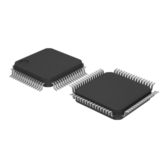
NUC502 2 Features 32-bit RISC CPU ARM7TDMI @ 81 MHz 16-bit Thumb mode supported to save code size Embedded 64 KB Local Memory divided into 32 segments for easier S/W programming Boot from SpiMemory or USB ... - Page 8 GNU-based, open-source IDE: compiler, linker and debugger Technology & Package 0.18um CMOS 3.3-volt single supply Dice form (NUC502)/LQFP-48 (NUC502ADN)/ LQFP-64 ( 10x10mm NUC502BDN) / LQFP-64 (7x7mm NUC502CDN) Apr 30, 2015 Page 8 of 266 Rev 1.1...
-
Page 9: Pad And Pin Configuration
NUC502 3 Pad and Pin Configuration NUC502ADN LQFP-48 Pin Out Apr 30, 2015 Page 9 of 266 Rev 1.1... - Page 10 NUC502 NUC502BDN NUC502CDN LQFP-64 Pin Out Apr 30, 2015 Page 10 of 266 Rev 1.1...
-
Page 11: Pin Descriptions
NUC502 Pin Descriptions In order to maximize the NUC502 application for different field, each pin of NUC502 is very flexible and can play up to four different functions. The user can program each pin to the wanted function for the different product. The pin functions are controlled by the registers PAD_REG0, PAG_REG1 and PAD_REG2. - Page 12 NUC502 Default Alternative Alternative Alternative Power on Function Function 1 Function 2 Function 3 setting Name GPA[8] SPIM0_SCK Power on set (IBR) GPA[9] SPIM0_SO Power on set (IBR) GPA[10] SPIM0_SI GPA[11] SPIMS_SI GPA[12] SPIMS_SO PWMT0 Power on set (IBR) Power on set GPA[13] SPIMS_SCK PWMT1...
- Page 13 NUC502 Default Alternative Alternative Alternative Power on Function Function 1 Function 2 Function 3 setting Name X12M EX12M X32K EX32K POWER VPP (6.5V) VBAT USBVDD33 DVDD33 DVDD33 AVDD33 DVSS DVSS DVSS AVSS VCC_CORE (OUTPUT) Pin Function for LQFP 64 nTRST GPC[0] SPIM1_SO USB_DET...
- Page 14 NUC502 Default Alternative Alternative Alternative Power on Function Function 1 Function 2 Function 3 setting Name GPC[5] PWMT2 UART1_TXD GPC[6] PWMT3 UART1_RXD GPC[7] PWMT0 UART1_CTS GPC[8] PWMT1 UART1_RTS GPC[9] PWMT2 I2C_DATA GPC[10] PWMT3 I2C_CLK Table4.1 Pin function Apr 30, 2015 Page 14 of 266 Rev 1.1...
- Page 15 NUC502 Symbol LQFP64 LQFP48 TYPE Description GPA[0] / 4/8mA I/O GPA[0] – General purpose AI[0] / with input/output digital pin MICP Analog input AI[0] – ADC analog input 0 MICP – MIC+ GPA[1] / 4/8mA I/O GPA[1] – General purpose AI[1] / with input/output digital pin...
- Page 16 NUC502 Symbol LQFP64 LQFP48 TYPE Description SPIMS_SO / input/output digital pin PWMT0 SPIMS_SO - Serial data output pin for SPIMS. PWMT0 – PWM output for timer GPA[13] / 4/8mA GPA[13] – General purpose SPIMS_SCK input/output digital pin SPIMS_SCK - Serial clock pin PWMT1 for SPIMS (master/slave).
- Page 17 NUC502 Symbol LQFP64 LQFP48 TYPE Description USB_DET / PWMT2 – PWM output for timer UART0_CTS USB_DET– USB detected input UART0_CTS – Clear to Send input pin for UART0 (High speed) GPB[4] / 12/16mA GPB[4] – General purpose PWMT3 / input/output digital pin USB_DET / PWMT3–...
- Page 18 NUC502 Symbol LQFP64 LQFP48 TYPE Description GPC[0] / 4/8mA GPC[0] – General purpose SPIM1_S0 / input/output digital pin USB_DET SPIM1_SO –Serial data output pin for SPIM1 (master) USB_DET– USB detected input GPC[1] / 4/8mA GPC[1] – General purpose SPIM1_SI / input/output digital pin USB_DET SPIM1_SI –Serial data input...
- Page 19 NUC502 Symbol LQFP64 LQFP48 TYPE Description PWMT2 / input/output digital pin I2C_DATA PWMT2 – PWM output for timer I2C_DATA – I2C data input/output pin, if this pin is select for I2C function GPC[10] / 4/8mA GPC[10] – General purpose PWMT3 / input/output digital pin I2C_CLK PWMT3 –...
- Page 20 NUC502 Symbol LQFP64 LQFP48 TYPE Description AVDD33 3.3V power supply for internal analog circuit VBAT 1.8V Power supply for internal RTC circuit VCC_CORE LDO 1.8V output pin OTP 6.5V VPP pin. For OTP write, this pin supply is 6.5V for read, this pin supply is 1.8V DVSS 18, 41, 13, 34,...
-
Page 21: System Diagram
NUC502 4 System Diagram 32.768kHz 12MHz Motor System Block Diagram X’tal Battery LDV/LVR 3.3V 1.8V ARM7TD USB Device 64KB SRAM TIME SPI Flash Securit RS232 37 GPIO’s Sensor Keypad Speaker Apr 30, 2015 Page 21 of 266 Rev 1.1... -
Page 22: Block Diagram
NUC502 5 Block Diagram 5.1 System Block Diagram ARM7TDMI SPIM x 2 TIMER Internal Boot ROM UART x 2 Internal SRAM USBPHY (64KB) GPIO Audio 8ch/10b - SARADC SPIMS Ctrl Mono 16 - bits DAC LVD, LDR Apr 30, 2015 Page 22 of 266 Rev 1.1... -
Page 23: On-Chip Bus Block Diagram
NUC502 5.2 On-Chip Bus Block Diagram NUC502 Bus Block Diagram 1.8V ARM7TDMI USBPHY CLKCTL Audio DAC SPIM ARM7 MISC Mono WRAPPER 16 - bits DAC APB - Bridge 6K Byte ROM 64K Byte SRAM 8ch/10b - SARADC LVD, LDR UART0 TIMER GPIO SPIMS... -
Page 24: Functional Description
NUC502 6 Functional Description 6.1 ARM7TDMI CPU Core The ARM7TDMI CPU core, a member of the Advanced RISC Machines (ARM) family of general-purpose 32-bit microprocessors, offers high performance with very low power consumption. The architecture is based on Reduced Instruction Set Computer (RISC) principles, and the instruction set and related decode mechanism are much simpler than those of micro-programmed Complex Instruction Set Computers. -
Page 25: System Manager
NUC502 6.2 System Manager 6.2.1 Overview The following functions are included in system manager section System memory map Bus arbitration algorithm Power-on setting Product identify register System control registers for reset/share pin/GPIO Clock control registers ... - Page 26 NUC502 Address Space Token Modules 0xB800_3000 – 0xB800_3FFF GPIO_BA GPIO Controller Registers 0xB800_4000 – 0xB800_4FFF I2C_BA I2C Interface Control Registers 0xB800_7000 – 0xB800_7FFF PWM_BA PWM Controller Registers 0xB800_8000 – 0xB800_8FFF RTC_BA Real Time Clock (RTC) Control Register 0xB800_A000 – 0xB800_AFFF SPIMS_BA SPI master/slave function Controller Registers 0xB800_B000 –...
-
Page 27: Ahb Bus Arbitration
NUC502 6.2.3 AHB Bus Arbitration The internal bus of NUC502 chip is an AHB-compliant Bus and supports to connect with the standard AHB master or slave. NUC502’s AHB arbiter provides a choice of two arbitration algorithms for simultaneous requests. These two arbitration algorithms are the d-priority mode and the round-robin-priority (rotate) mode. -
Page 28: Power-On Settings
NUC502 Round Robin Priority Mode 6.2.4.1 Round-robin priority mode is selected if PRTMODx = 1. The AHB bus arbiter uses a round robin arbitration scheme for every master module to gain the bus ownership in turn. That is the requestor having the highest priority becomes the lowest-priority requestor after it has been granted access. -
Page 29: System Manager Control Registers
NUC502 6.2.6 System Manager Control Registers Default Register Address Description Value GCR_BA = 0xB100_0000 PDID GCR_BA+0x00 Product Identification Register 0x0055_0502 System Power-On Configuration SPOCR GCR_BA+0x04 0x0000_00XX Register CPUCR GCR_BA+0x08 CPU Control Register 0x0000_0000 MISCR GCR_BA+0x0C Miscellaneous Control Register 0x0000_0000 IPRST GCR_BA+0x14 IP Reset Control Resister 0x0000_0000... - Page 30 NUC502 Bits Descriptions [31:24] Reserved Reserved Chip Version Identifier [27:24] Chip version identifier is “4’h0” for 1 version Chip Identifier [23:0] Chip identifier is “24’h55_0502” for NUC502. System Power On Configuration Register (SPOCR) This register provides specific information for software to identify this chip’s power-on setting.
- Page 31 NUC502 Bits Descriptions SPI flash speed selection (SCLK) 00 : 72 MHz [6:5] SYS_CFG 01 : 36 MHz 10 : 18 MHz 11 : 50 KHz ICE Mode configuration setting (Read Only) 0: ICE mode enable and the disable the cipher function 1: Normal mode LQFP48 ICE mode configuration setting 0: 48-pins package and GPB[9:5] for ICE connection...
- Page 32 NUC502 Bits Descriptions [31:1] Reserved Reserved CPU one shut reset. Write this bit 1 will reset the CPU. This bit will auto clear after the CPU reset CPURST 0 : Normal 1 : Reset CPU MISC Control Register (MISCR) Register Address Description Reset Value...
- Page 33 NUC502 IP Reset Control Register (IPRST) This register provides specific read-only information for software to identify this chip. Default Register Address Description Value IPRST GCR_BA+14 IP Reset Control Resister 0x0000_0000 Reserve SPIMS_RS Reserve ADC_RS GPIO_RS Reserved SRAM_RS Reserved Reserved APU_RST Reserved UDC_RST SPIM_RS...
- Page 34 NUC502 Bits Descriptions APU controller Reset [16] APU_RST “0”: Normal operation “1”: IP reset [15:12] Reserved Reserved USB Device controller Reset [11] UDC_RST “0”: Normal operation “1”: IP reset SPIM0 and SPI1 controller Reset [10] SPIM_RST “0”: Normal operation “1”: IP reset I2C controller Reset I2C_RST “0”: Normal operation...
- Page 35 NUC502 Reserved Reserved Reserved Reserved IPACT IPEN Reserved PRTMOD0 Bits Descriptions [31:6] Reserved Reserved Interrupt active status in IPEN enabled mode This bit is set when the IPEN is enabled and the external FIQ or IRQ IPACT is active Write “1” to clear the status 0: Inactive 1: Active Enable raising the Priority of CPU in IRQ or FIQ period...
- Page 36 NUC502 PWM_TMR3_I PWM_TMR3_O PWM_TMR2_I PWM_TMR2_O PWM_TMR1_I PWM_TMR1_O PWM_TMR0_I PWM_TMR0_O Bits Descriptions PWM Timer 3 input pin selection 000 = PWM Timer 3 input from GPIOB[0] 001 = PWM Timer 3 input from GPIOB[4] [31:29] PWM_TMR3_I 010 = PWM Timer 3 input from GPIOC[6] 011 = PWM Timer 3 input from GPIOC[10] 100 = PWM Timer 3 input from GPIOB[7] Others : disable PWM Timer 3 input function...
- Page 37 NUC502 Bits Descriptions PWM Timer 2 output pin selection 1 = output enable 0 = output disable [16] = PWM Timer 2 output to GPIOA[15] PWM_TMR2_O [20:16] [17] = PWM Timer 2 output to GPIOB[3] [18] = PWM Timer 2 output to GPIOC[5] [19] = PWM Timer 2 output to GPIOC[9] [20] = PWM Timer 2 output to GPIOB[6] PWM Timer 1 input pin selection...
- Page 38 NUC502 Register Address Description Reset Value PAD_REG1 GCR_BA+34 PAD Control Register 0x0000_0000 Reserved ADCP_EN Reserved UART1_M UART0_M Reserv UART1_ UART0_ Reserv SPIM0_ SPIMS_ SPIM1_EN I2CP_EN ICE_EN Bits Descriptions [31:24] Reserved Reserved ADC pins enable [23:16] represents GPIOA[7:0] respectively [23:16] ADCP_EN 0 = disable 1 = enable [15:13]...
- Page 39 NUC502 Bits Descriptions SPIM0 pin enable GPIOA[10:8] used as pins of the SPIM0 (SPI_ROM) SPIM0_EN 0 = disable 1 = enable SPIMS pin enable (SPIMS pins at GPIOA[14:11]) GPA[14] used as the CS_ pin of SPIMS, and was controlled by SPIMS_EN SPIMS CNTRL[16] 0 = disable...
- Page 40 NUC502 Reserved USBDET_SEL Bits Descriptions [31:4] Reserved Reserved USB detection selection 0000 : disable 0001 : USB connection detect pin from GPA[14] 0010 : USB connection detect pin from GPA[15] 0011 : USB connection detect pin from GPB[0] 0100 : USB connection detect pin from GPB[1] 0101 : USB connection detect pin from GPB[2] 0110 : USB connection detect pin from GPB[3] [3:0]...
- Page 41 NUC502 Bits Descriptions [31:16] Reserved Reserved GPIOA driving strength [15:0] GPA_DS 0: 4mA driving strength IO 1: 8mA driving strength IO GPIOB driving strength (GPB_DS) Reset Register Address Description Value GPB_DS GCR_BA+78 GPIOB driving strength 0x0000_0000 Reserved Reserved Reserved GPB_DS[9:8] GPB_DS[7:0] Bits Descriptions...
- Page 42 NUC502 Reset Register Address Description Value GPC_DS GCR_BA+7C GPIOC driving strength 0x0000_0000 Reserved Reserved Reserved GPC_DS[10:8] GPC_DS[7:0] Bits Descriptions [31:11] Reserved Reserved GPIOC driving strength [10:0] GPC_DS 0: 4mA driving strength IO 1: 8mA driving strength IO Apr 30, 2015 Page 42 of 266 Rev 1.1...
-
Page 43: Clock Controller
NUC502 6.3 Clock Controller 6.3.1 Function Description The clock controller generates the clocks for the whole chip, it include all AMBA interface modules and all peripheral clocks, the USB, UART, APU and so on. There is one PLL modules in this chip, and the PLL clock source is from the external crystal input. 1/ADC_N ADC_CK_EN 1/APB_N... -
Page 44: Clock Control Registers
NUC502 6.3.2 Clock Control Registers Register Address Description Reset Value CLK_BA = 0xB100_0200 PWRCON CLK_BA + 00 R/W System Power Down Control Register 0x00FF_FF03 AHB Device Clock Enable Control AHBCLK CLK_BA + 04 0x0000_0083 Register APB Device Clock Enable Control APBCLK CLK_BA + 08 0x0000_0007... - Page 45 NUC502 Power Down Control Register (PWRCON) The chip clock source is from an external crystal. The crystal oscillator can be control on/off by the register XTAL_EN. When turn off the crystal, the chip into power down state. Crystal wake up pre-scale counter value. After the clock counter count pre-scale × 256 crystal cycle, the clock controller output the clock to system.
- Page 46 NUC502 Bits Descriptions Crystal to stable. 1 = Enable the pre-scale counter 0 = Disable the pre-scale, assume the crystal is stable Crystal Oscillator (Power Down) Control XTAL_EN 1: Crystal oscillation enable (Normal operation) 0: Crystal oscillation disable (Power down) Apr 30, 2015 Page 46 of 266 Rev 1.1...
- Page 47 NUC502 AHB Devices Clock Enable Control Register (AHBCLK) These register bits are used to enable/disable clock for AMBA clock, AHB engine and peripheral Register Address Description Reset Value AHB Devices Clock Enable Control AHBCLK CLK_BA + 04 0x0000_0083 Register Reserved Reserved Reserved APU_CK_EN...
- Page 48 NUC502 APB Devices Clock Enable Control Register (APBCLK) These register bits are used to enable/disable clock for APB engine and peripheral. Register Address Description Reset Value APB Devices Clock Enable Control APBCLK CLK_BA + 08 0x0000_0007 Register Reserved Reserved ADC_CK_E SPIMS_CK_E Reserved Reserve...
- Page 49 NUC502 Bits Descriptions Real-Time-Clock APB interface Clock Control. This bit is used to control the APB clock only, The RTC engine clock source is from the RTC_CK_EN 32.768 KHz crystal input. 0 = Disable 1 = Enable Watch Dog Clock Enable. The Watch Dog engine clock source is from the crystal input WD_CK_EN 0 = Disable...
- Page 50 NUC502 Clock Source Select Control Register (CLKSEL) Before clock switch the related clock sources (pre-select and new-select) must be turn on. Register Address Description Reset Value CLKSEL CLK_BA + 10 R/W Clock Source Select Control Register 0x0000_0000 Reserved Reserved ADC_S Reserved UART_S APU_S...
- Page 51 NUC502 Bits Descriptions HCLK clock source select. [1:0] 00: clock source from crystal clock in. [1:0] HCLK_S 01: clock source from divided MPLL clock 10: clock source from divided MPLL clock / 2 11: clock source from crystal 32k input Apr 30, 2015 Page 51 of 266 Rev 1.1...
- Page 52 NUC502 Clock Divider Register0 (CLKDIV0) Register Address Description Reset Value CLKDIV0 CLK_BA_+ 14 R/W Clock Divider Number Register 0x0000_0000 Reserved USB_N UART_N APU_N APB_N Reserved HCLK_N Bits Descriptions [31:24] Reserved Reserved USB clock divide number from USB clock source [23:20] USB_N The USB clock frequency = (USB clock source frequency ) / (USB_N + 1) UART clock divide number from UART clock source [19:16] UART_N...
- Page 53 NUC502 ADC_N Reserved Reserved Bits Descriptions [31:24] Reserved Reserved ADC engine clock divide number from ADC clock source [23:16] ADC_N The ADC engine clock frequency = (ADC engine clock source frequency ) / (ADC_N + 1) [15:0] Reserved Reserved Apr 30, 2015 Page 53 of 266 Rev 1.1...
- Page 54 NUC502 MPLL Control Register (MPLLCON) The MPLL reference clock input is directly from the external clock input, and the other PLL control inputs are connected to bits of the registers. Register Address Description Reset Value MPLLCON CLK_BA + 20 R/W MPLL Control Register 0x0001_4035 Reserved Reserved...
- Page 55 NUC502 Output Clock Frequency Setting FOUT Constrain: preferred FOUT Output Clock Frequency Input (Reference) Clock Frequency Input Divider (2 x (IN_DV + 2)) Feedback Divider (2 x (FB_DV + 2)) OUT_DV = “00”...
-
Page 56: Spi Synchronous Serial Interface Controller (Master Mode)
NUC502 6.4 SPI Synchronous Serial Interface Controller (Master Mode) 6.4.1 Overview The SPI Synchronous Serial Interface controller performs a serial-to-parallel conversion on data received from the peripheral, and a parallel-to-serial conversion on data received from CPU. This controller can drive up to 2 external peripherals and is seen as the master. It can generate an interrupt signal when data transfer is finished and can be cleared by writing 1 to the interrupt flag. -
Page 57: Spim Timing Diagram
NUC502 6.4.3 SPIM Timing Diagram The timing diagram of SPI transaction is shown as following: spi_ss_o spi_sclk_o spi_so_o Tx[6] Tx[5] Tx[4] Tx[3] Tx[2] Tx[1] (Tx[7]) (Tx[0]) spi_si_i Rx[6] Rx[5] Rx[4] Rx[3] Rx[2] Rx[1] (Rx[7]) (Rx[0]) CNTRL[LSB]=0, CNTRL[Tx_NUM]=0x0, CNTRL[Tx_BIT_LEN]=0x08, CNTRL[Tx_NEG]=1, CNTRL[Rx_NEG]=0, SSR[SS_LVL]=0 SPI Timing 6.4.4 SPIM Programming Example without DMA If you want to access a device with following specifications:... -
Page 58: Spim Programming Example With Dma
NUC502 6.4.5 SPIM Programming Example with DMA If users want to access a device with DMA function, 3 additional registers need to be configured. They are CODE_LEN, AHB_ADDR and SPI_ADDR. DMA function can be used to support loading boot code, reading data from system memory into peripherals or copy data from peripherals, reading data from peripherals into system memory. -
Page 59: Direct Memory Mapping Mode
NUC502 7. Set SPI_CNTRL = 0x161345 for control information. 8. Wait code write finish. Wait interrupt 9. Set SSR register to un-select spi slave. ( no support ASS in dma mode ) 10. Check the BUSY status in SPI Flash 6.4.6 Direct memory mapping mode Users can see SPI flash as a ROM when in direct memory mapping mode. -
Page 60: Spim Serial Interface Control Registers Mapping
NUC502 6.4.7 SPIM Serial Interface Control Registers Mapping R: read only, W: write only, R/W: both read and write, C: Only value 0 can be written Register Address R/W/C Description Reset Value Base Address: 0xB100_7000 CNTRL SPI_BA + 0x00 Control and Status Register 0x0000_0004 DIVIDER SPI_BA + 0x04... - Page 61 NUC502 Control and Status Register (CNTRL) Register Address R/W/C Description Reset Value SPI_BA + CNTRL Control and Status Register 0x0000_0004 0x00 SPI_MODE COMMAND DIS_M BOOT_SPI F_DRD F_TYPE Insert_ SLEEP Tx_NUM dummy Tx_BIT_LEN Tx_NEG Rx_NEG GO_BUSY Descriptions Bits SPI read mode selection 8’h03: standard read mode [31:24] SPIM_MODE...
- Page 62 NUC502 Descriptions Bits NOTE: When want to access SPI flash through direct memory mapping, please set this bit high. SPI ROM Boot /Page Write enable 0 = Disable ROM boot or page write operation. [20] BOOT_SPIM 1 = Enable ROM boot or page write operation. NOTE: When want to access SPI flash through direct memory mapping, please set this bit high.
- Page 63 NUC502 Descriptions Bits default value is 0x0. When CNTRL[Tx_NUM] = 00, setting this field has no effect on transfer. The desired interval is obtained according to the following equation (from the last falling edge of current sclk to the first rising edge of next sclk): (CNTRL[SLEEP] + 2)*period of SCLK SLEEP = 0x0 …...
- Page 64 NUC502 Descriptions Bits one transfer. 11 = Four successive transmit/receive will be executed in one transfer. Transmit Bit Length This field specifies how many bits are transmitted in one transmit/receive. Up to 32 bits can be transmitted. Tx_BIT_LEN = 0x01 … 1 bit [7:3] Tx_BIT_LEN Tx_BIT_LEN = 0x02 …...
- Page 65 NUC502 Divider Register (DIVIDER) Register Address R/W/C Description Reset Value SPIM_BA + DIVIDER Clock Divider Register 0x0000_0000 0x04 Reserved Reserved SCLK_IN_DLY IDLE_CNT DIVIDER[15:8] DIVIDER[7:0] Bits Descriptions [31:23] Reserved Reserved Serial CLK Input Delay register Set this register to adjust the spi_sclki clock input delay. There are total 8 buffers in this delay path.
- Page 66 NUC502 Bits Descriptions NOTE: When set DIVIDER to zero, SPI clock will be equal to engine clock. NOTE: when set DIVIER to zero, sleep(CNTRL[SLEEP]) can’t set to zero. Apr 30, 2015 Page 66 of 266 Rev 1.1...
- Page 67 NUC502 Slave Select Register (SSR) Register Address R/W/C Description Reset Value SPIM_BA + Slave Select Register 0x0000_0000 0x08 Reserved Reserved Reserved Reserved SS_LVL Reserved Bits Descriptions [31:4] Reserved Reserved Automatic Slave Select 0 = If this bit is cleared, slave select signals are asserted and de-asserted by setting and clearing related bits in SSR register.
- Page 68 NUC502 Bits Descriptions If SSR[ASS] bit is cleared, writing 1 to any bit location of this field sets the proper spi_ss_o line to an active state and writing 0 sets the line back to inactive state. If SSR[ASS] bit is set, writing 1 to any bit location of this field will select appropriate spi_ss_o line to be automatically driven to active state for the duration of the transmit/receive, and will be driven to inactive state for the rest of the time.
- Page 69 NUC502 Data Receive Register 0/1/2/3 (RX0/0/2/3) Register Address R/W/C Description Reset Value SPIM_BA + Data Receive Register 0 0x0000_0000 0x10 SPIM_BA + Data Receive Register 1 0x0000_0000 0x14 SPIM_BA + Data Receive Register 2 0x0000_0000 0x18 SPIM_BA + Data Receive Register 3 0x0000_0000 0x1C Rx [31:24]...
- Page 70 NUC502 Data Transmit Register 0/1/2/3 (TX0/1/2/3) Register Address R/W/C Description Reset Value SPIM_BA + Data Transmit Register 0 0x0000_0000 0x20 SPIM_BA + Data Transmit Register 1 0x0000_0000 0x24 SPIM_BA + Data Transmit Register 2 0x0000_0000 0x28 SPIM_BA + Data Transmit Register 3 0x0000_0000 0x2C Tx [31:24]...
- Page 71 NUC502 AHB Address Register (AHB_ADDR) Register Address R/W/C Description Reset Value SPIM_BA + AHB_ADDR AHB address Register 0x0000_0000 0x30 AHB_ADDR AHB_ADDR AHB_ADDR AHB_ADDR Bits Descriptions AHB address [31:0] AHB_ADDR This is the system memory address when in DMA mode. Code Length Register (CODE_LEN) Register Address R/W/C Description...
- Page 72 NUC502 SPIM_ADDR SPIM_ADDR SPIM_ADDR Reserved Bits Descriptions [31:24] Reserved Reserved SPI Flash start access address [23:2] SPIM_ADDR Note: SPI Flash starting address must be word alignment [1:0] Reserved Reserved Apr 30, 2015 Page 72 of 266 Rev 1.1...
-
Page 73: Audio Processing Unit
NUC502 6.5 Audio Processing Unit The main purpose of Audio Processing Unit (APU) is used to playback the audio data (PCM format) which CPU decoded and stored in global RAM. The APU built in a monophonic DAC with 16-bit resolution per channel which supports speakerphone output and monophonic output for headphone. -
Page 74: Apu Control Register Mapping
NUC502 input data is 48KHz, the AUDIO_DAC clock should be set to 6.144Mhz. Therefore, CLKSEL[5:4] and CLKDIV0[15:8] should be set a proper value to divide the clock source by about 26 (166/6.144)). We my set CLKSEL[5:4]=2’b01 and set CLKDIV0[15:8]=0x19. 2. Set base address and threshold addresses The APU implement the ping-pong buffer mechanism and the buffers are ... -
Page 75: Apu Control Registers
NUC502 6.5.6 APU Control Registers APU Control Register Register Address Description Reset Value APUCON APU_BA+0x00 R/W APU Control Register 0x0000_0000 Reserved Reserved APURST Reserved Reserved APURUN Bits Descriptions [31:17] Reserved Reserved APU Reset [16] APURST 0 = No action 1 = Reset the whole ADC except register value. [15:1] Reserved Reserved... - Page 76 NUC502 Parameter Control Register Register Address Description Reset Value PARCON APU_BA+0x04 R/W Parameter Control Register 0x0000_0001 Reserve Reserved ZERO_EN Reserved SWAP Reserved Reserved Bits Descriptions [31:26] Reserved Reserved Zero cross detection enable [25] ZERO_EN 0 = Disable 1 = Enable Reserved [24] Reserved...
- Page 77 NUC502 APU Power Down Control Register Register Address Description Reset Value PDCON APU_BA+0x08 R/W Power Down Control Register 0x0001_0000 Reserved Reserved ANA_PD Reserved Reserved Bits Descriptions [31:17] Reserved Reserved Audio DAC Power Down [16] ANA_PD 0 = Normal operation 1 = Power down [15:0] Reserved Reserved...
- Page 78 NUC502 APU Interrupt Register Register Address Description Reset Value APUINT APU_BA+0x0C R/W APU Interrupt Register 0x0000_0000 Reserved Reserved T2INTEN T1INTEN Reserved Reserved T2INTS T1INTS Bits Descriptions [31:18] Reserved Reserved Threshold 2 Interrupt Enable [17] T2INTEN 0 = Disable 1 = Enable Threshold 1 Interrupt Enable [16] T1INTEN...
- Page 79 NUC502 RAM Base Address Register Register Address R/W Description Reset Value RAMBSAD APU_BA+0x10 R/W RAM Base Address Register 0x0000_0000 BSAD[31:24] BSAD[23:16] BSAD[15:8] BSAD[7:0] Bits Descriptions [31:0] BSAD Global RAM Base Address Apr 30, 2015 Page 79 of 266 Rev 1.1...
- Page 80 NUC502 Threshold 1 Address Register Register Address Description Reset Value THAD1 APU_BA+0x14 R/W Threshold 1 Address Register 0x0000_0000 TH1[31:24] TH1[23:16] TH1[15:8] TH1[7:0] Bits Descriptions [31:0] Threshold 1 Address Apr 30, 2015 Page 80 of 266 Rev 1.1...
- Page 81 NUC502 Threshold 2 Address Register Register Address Description Reset Value THAD2 APU_BA+0x18 R/W Threshold 2 Address Register 0x0000_0000 TH2[31:24] TH2[23:16] TH2[15:8] TH2[7:0] Bits Descriptions [31:0] Threshold 2 Address 0x00000000 Internal SRAM RAM Base Address Threshold 1 Address Threshold 2 Address Apr 30, 2015 Page 81 of 266 Rev 1.1...
- Page 82 NUC502 Current Address Register Register Address Description Reset Value CURAD APU_BA+0x1C Current Access RAM Address Register 0x0000_0000 CURAD[31:24] CURAD[23:16] CURAD[15:8] CURAD[7:0] Bits Descriptions [31:0] CURAD Current APU Access RAM Address Apr 30, 2015 Page 82 of 266 Rev 1.1...
-
Page 83: Sram Controller
NUC502 6.6 SRAM Controller 6.6.1 Overview The SRAM controller is design for program code and data storage. It’s an AHB slave and SRAM size is up to 64KB. This 64KB memory is separated into 32 memory block and the size of each memory block is 2KB. Each memory block could be randomly mapped to any 2KB space of 0x0000_0000 ~ 0x1FFF_FFFF of system memory by modifying the control register. -
Page 84: Sram Block Diagram
NUC502 6.6.3 SRAM Block Diagram The block diagram of SRAM Controller is depicted as following: AHB BUS AHB Slave Wrapper I/O Decoder & TAG Control Register SRAM0 SRAM8 SRAM16 SRAM24 SRAM1 SRAM9 SRAM17 SRAM25 SRAM2 SRAM10 SRAM18 SRAM26 SRAM3 SRAM11 SRAM19 SRAM27 SRAM4... -
Page 85: Sram System Diagram
NUC502 6.6.4 SRAM System Diagram The following diagram briefs the related circuit with SRAM Controller: AHB Bus Clock Reset SRAM Controller Controller Controller Apr 30, 2015 Page 85 of 266 Rev 1.1... -
Page 86: Sram Function Description
NUC502 6.6.5 SRAM Function Description It’s an AHB slave and SRAM size is up to 64KB. The 64KB memory is separated into 32 memory block and the size of each memory block is 2KB. Each memory block could be randomly mapped to any 2KB space of 0x0000_0000 ~ 0x1FFF_FFFF of system memory. For this purpose, 32 tag registers are implemented to keep the base address of each 2KB memory block. -
Page 87: Sram Register Mapping
NUC502 6.6.6 SRAM Register Mapping Register Address Description Reset Value SRAMCTRL_BA = 0xB100_4000 SCTRL0 SRAMCTRL_BA + SRAM Control Register 0 0x0000_0001 SCTRL1 SRAMCTRL_BA + SRAM Control Register 1 0x0000_0801 SCTRL2 SRAMCTRL_BA + SRAM Control Register 2 0x0000_1001 SCTRL3 SRAMCTRL_BA + SRAM Control Register 3 0x0000_1801 SCTRL4... - Page 88 NUC502 SCTRL22 SRAMCTRL_BA + SRAM Control Register 22 0x0000_B001 SCTRL23 SRAMCTRL_BA + SRAM Control Register 23 0x0000_B801 SCTRL24 SRAMCTRL_BA + SRAM Control Register 24 0x0000_C001 SCTRL25 SRAMCTRL_BA + SRAM Control Register 25 0x0000_C801 SCTRL26 SRAMCTRL_BA + SRAM Control Register 26 0x0000_D001 SCTRL27 SRAMCTRL_BA +...
- Page 89 NUC502 Register Descriptions 6.6.6.1 SRAM Control Register 0 (SCTRL0 ~ SCTRL15) Register Address R/W/C Description Reset Value SCTRL0 SRAMCTRL_BA+0x000 R/W SRAM Control Register 0 0x0000_0001 SCTRL1 SRAMCTRL_BA+0x004 R/W SRAM Control Register 1 0x0000_0801 SCTRL2 SRAMCTRL_BA+0x008 R/W SRAM Control Register 2 0x0000_1001 SCTRL3 SRAMCTRL_BA+0x00C R/W SRAM Control Register 3...
- Page 90 NUC502 SCTRL30 SRAMCTRL_BA+0x078 R/W SRAM Control Register 30 0x0000_F001 SCTRL31 SRAMCTRL_BA+0x07C R/W SRAM Control Register 31 0x0000_F801 Reserved Reserved Reserved VALID Bits Descriptions [31:29] Reserved Reserved TAG Address This field keeps the base address of each 2KB memory block. Once the [28:11] address bits [28:11] from system bus are the same with the content of this filed, and the VALID flag is enabled, the related memory block will be...
-
Page 91: Usb Device Controller
NUC502 6.7 USB Device Controller 6.7.1 Overview The USB device is an interface that transmits and receives data packets between host and USB device controller. It also handles the routing data between the bus interface and various endpoints on the device controller. On the device controller, it includes the AHB bus and USB bus which comes from the USB PHY transceiver. -
Page 92: Functional Descriptions
NUC502 6.7.3 Functional Descriptions SIE (Serial Interface Engine) 6.7.3.1 The SIE is the front-end of the device controller and handles most of the USB packet protocol. The SIE typically comprehends signaling up to the transaction level. The functions that it handles could include: Packet recognition, transaction sequencing SOP, EOP, RESET, RESUME signal detection/generation Clock/Data separation... -
Page 93: Memory Mapping
NUC502 Interrupt 6.7.3.5 This USB provides 1 interrupt source with 4 interrupt events (WAKEUP, FLO, USB, BUS). WAKEUP interrupt is for stop wakeup only, FLO interrupt is for USB plug-in or unplug, USB event notifies users of some USB requests, like IN ACK, OUT ACK etc., and BUS event notifies users of some bus events, like suspend, resume, etc. - Page 94 NUC502 Register Address R/W Description Reset Value BUFSEG USB_BA+0x018 R/W Buffer Segmentation 0x0000_0000 BUFSEG0 USB_BA+0x020 R/W Buffer Segmentation of endpoint 0 0x0000_0000 MXPLD0 USB_BA+0x024 R/W Maximal payload of endpoint 0 0x0000_0000 CFG0 USB_BA+0x028 R/W Configuration of endpoint 0 0x0000_0000 stall control register and In/out ready CFGP0 USB_BA+0x02C R/W 0x0000_0000...
- Page 95 NUC502 Interrupt Enable Register (IEF) Register Address Description Reset Value USB_BA+0x000 R/W Interrupt Enable Flag 0x0000_0000 Reserved Reserved INNAKEN Reserved WAKEFUEN Reserved WAKEUPEN FLDEN USBEN BUSEN Bits Descriptions [31:16] Reserved Reserved 0 = Disable IN NAK INT (Write Only) [15] INNAKEN 1 = Enable [14:9]...
- Page 96 NUC502 Interrupt Event Flag Register (EVF) This register is USB Interrupt Event Flag register, clear by read STS, ATTR or FLODET. Register Address Description Reset Value USB_BA+0x004 R/W Interrupt Event Flag 0x0000_0000 Setup Reserved Reserved EPTF5 EPTF4 EPTF3 EPTF2 EPTF1 EPTF0 Reserved Reserved...
- Page 97 NUC502 Bits Descriptions [15:4] Reserved Reserved WAKEUP Wake up event occurred, cleared by write 1 to EVF[3] Floating detect event occurred, cleared by write 1 to EVF[2]. USB event occurred, check STS[6:4] or STS0~5[2:0] to know which kind of USB event was occurred, cleared by write 1 to EVF[1] or EPTF0~5 and Setup = 0.
- Page 98 NUC502 Reserved STS5 STS5 STS4 STS3 STS2 STS2 STS1 STS0 Overrun Bits Descriptions [31:26] Reserved Reserved System states of endpoint 5 000: In ACK 001: In NAK [25:23] STS5 010: Out 0 ACK 110: Out 1 ACK 011: Setup ACK 111: Isochronous translation end System states of endpoint 4 000: In ACK...
- Page 99 NUC502 Bits Descriptions System states of endpoint 2 000: In ACK 001: In NAK [16:14] STS2 010: Out 0 ACK 110: Out 1 ACK 011: Setup ACK 111: Isochronous translation end System states of endpoint 1 000: In ACK 001: In NAK [13:11] STS1 010: Out 0 ACK...
- Page 100 NUC502 Reserved enUSB Reserved RWakeup enPHY Timeout Resume Suspend usbRST Bits Descriptions [31:8] Reserved Reserved 0 = Disable USB enUSB 1 = Enable Reserved Reserved 0 = Nothing RWakeUp 1 = force USB bus to K state, used for remote wake-up. 0 = Disable PHY enPHY 1 = Enable...
- Page 101 NUC502 Floating detection Register (FLODET) Register Address Description Reset Value FLODET USB_BA+0x014 R Floating detection 0x0000_0000 Reserved Reserved Reserved Reserved FLODET Bits Descriptions [31:1] Reserved Reserved 0 = floating FLODET 1 = connected Buffer Segmentation Register (BUFSEG) For Setup token only. Register Address Description Reset Value...
- Page 102 NUC502 For Setup token only. [8:3] BUFSEG Effective starting address USB buffer = {BUFSEG[8:3], 3’b000} [2:0] Reserved Reserved Buffer Segmentation Register (BUFSEGx) x = 0~5 Register Address Description Reset Value BUFSEG0 USB_BA+0x020 R/W Buffer segmentation of endpoint 0 0x0000_0000 BUFSEG1 USB_BA+0x030 R/W Buffer segmentation of endpoint 1 0x0000_0000 BUFSEG2 USB_BA+0x040 R/W...
- Page 103 NUC502 Maximal Payload Register (MXPLDx) x = 0~5 Register Address Description Reset Value MXPLD0 USB_BA+0x024 R/W Maximal Payload of endpoint 0 0x0000_0000 MXPLD1 USB_BA+0x034 R/W Maximal Payload of endpoint 1 0x0000_0000 MXPLD2 USB_BA+0x044 R/W Maximal Payload of endpoint 2 0x0000_0000 MXPLD3 USB_BA+0x054 R/W Maximal Payload of endpoint 3...
- Page 104 NUC502 Configuration Register (CFGx) x = 0~5 Register Address Description Reset Value CFG0 USB_BA+0x028 R/W Configuration of Endpoint 0 0x0000_0000 CFG1 USB_BA+0x038 R/W Configuration of Endpoint 1 0x0000_0000 CFG2 USB_BA+0x048 R/W Configuration of Endpoint 2 0x0000_0000 CFG3 USB_BA+0x058 R/W Configuration of Endpoint 3 0x0000_0000 CFG4 USB_BA+0x068 R/W...
- Page 105 NUC502 Extra Configuration Register (CFGPx) x = 0~5 Register Address Description Reset Value stall control register and In/out CFGP0 USB_BA+0x02C R/W 0x0000_0000 ready clear flag of endpoint 0 stall control register and In/out CFGP 1 USB_BA+0x03C R/W 0x0000_0000 ready clear flag of endpoint 1 stall control register and In/out CFGP 2 USB_BA+0x04C R/W...
- Page 106 NUC502 USBSE0 Register Address Description Reset Value USBSE0 USB_BA+0x090 R/W Set D+ and D- to idle state 0x0000_0000 Reserved Reserved Reserved Reserved Bits Descriptions [31:1] Reserved Reserved 0: Normal state 1: SE0 state In SE0 state, the USB D+ and D- will be drive low and cause host doesn’t see the device even the USB cable is still connected.
-
Page 107: Advanced Interrupt Controller
NUC502 6.8 Advanced Interrupt Controller 6.8.1 Overview An interrupt temporarily changes the execution sequence of a program to react to a particular event such as power failure, watchdog timer timeout, and engine complete, system events, external event trigger and so on. The ARM processor provides two modes of interrupts, the Fast Interrupt (FIQ) mode for critical session and the Interrupt (IRQ) mode for general purpose. -
Page 108: Interrupt Sources
NUC502 6.8.3 Interrupt Sources The following table lists all interrupts from various peripheral interface modules or external devices. Reset Channel Name Source (default) level WDT_INT SCR1[15:8] Watch Dog Timer Interrupt Reserved Reserved Reserved INT_GPIO0 SCR1[31:24] GPIO Interrupt0 INT_GPIO1 SCR2[7:0] GPIO Interrupt1 INT_GPIO2 SCR2[15:8] GPIO Interrupt2... - Page 109 NUC502 INT_PWM2 SCR7[7:0] PWM Interrupt2 INT_PWM3 SCR7[15:8] PWM Interrupt3 INT_I2C SCR7[23:16] I2C Interface Interrupt INT_SPIMS SPI (Master/Slave) Serial SCR7[31:24] Interface Interrupt Reserved Reserved Reserved INT_PWR SCR8[15:8] System Wake-Up Interrupt INT_SPIM SCR8[23:16] SPIM0/1 Interrupt Reserved Reserved Reserved SPIM SPIMS PWM3 PWM2 PWM1 PWM0 TMR0...
-
Page 110: Aic Functional Descriptions
NUC502 6.8.4 AIC Functional Descriptions Hardware Interrupt Vectoring The hardware interrupt vectoring can be used to shorten the interrupt latency. If not used, priority determination must be carried out by software. When the Interrupt Priority Encoding Register (AIC_IPER) is read, it will return an integer representing the channel that is active and having the highest priority. - Page 111 NUC502 Interrupt Masking Each interrupt source can be enabled or disabled individually by using the command registers AIC_MECR and AIC_MDCR. The status of interrupt mask can be read in the read only register AIC_IMR. A disabled interrupt doesn’t affect the servicing of other interrupts. Interrupt Clearing and Setting All interrupt sources can be individually set or clear by respectively writing to the registers AIC_SSCR and AIC_SCCR when they are programmed to be edge triggered.
-
Page 112: Aic Registers Mapping
NUC502 The following table shows the main steps of an interrupt and the order in which they are performed according to the mode: Action Normal Mode ICE/Debug Mode Calculate active interrupt Read AIC_IPER Read AIC_IPER Determine and return the vector of Read AIC_IPER Read AIC_IPER the active interrupt... - Page 113 NUC502 AIC_ISR AIC_BA+108 Interrupt Status Register 0x0000_0000 AIC_IPER AIC_BA+10C Interrupt Priority Encoding Register 0x0000_0000 AIC_ISNR AIC_BA+110 Interrupt Source Number Register 0x0000_0000 AIC_IMR AIC_BA+114 Interrupt Mask Register 0x0000_0000 AIC_OISR AIC_BA+118 Output Interrupt Status Register 0x0000_0000 Reserved Reserved Reserved Undefined AIC_MECR AIC_BA+120 Mask Enable Command Register Undefined AIC_MDCR AIC_BA+124...
-
Page 114: Aic Control Registers
NUC502 6.8.6 AIC Control Registers AIC Source Control Registers (AIC_SCR1 ~ AIC_SCR8) Register Address R/W/C Description Reset Value AIC_SCR1 AIC_BA+000 Source Control Register 1 ~ 0x4747_4747 Source Control Register 8 AIC_SCR8 AIC_BA+01C TYPE (Channel 3) Reserved PRIORITY (Channel 3) TYPE (Channel 2) Reserved PRIORITY (Channel 2) TYPE (Channel 1) - Page 115 NUC502 Bits Descriptions Priority Level (0 – 7) The level 0 indicates the highest priority and the level 7 indicates the lowest priority. [26:24] An interrupt is treated as a FIQ mode for the priority level 0, and [18:16] PRIORITY is treated as an IRQ mode for other levels.
- Page 116 NUC502 AIC Interrupt Raw Status Register (AIC_IRSR) Register Address Description Reset Value AIC_IRSR AIC_BA+100 Interrupt Raw Status Register 0x0000_0000 IRS[31:24] IRS[23:16] IRS[15:8] IRS[7:0] This register records the intrinsic state within each interrupt channel. Bits Descriptions Interrupt Status Indicate the intrinsic status of the corresponding interrupt source [31:0] IRS x ...
- Page 117 NUC502 AIC Interrupt Active Status Register (AIC_IASR) Register Address Description Reset Value AIC_IASR AIC_BA+104 Interrupt Active Status Register 0x0000_0000 IAS[31:24] IAS[23:16] IAS[15:8] IAS[7:0] This register indicates the status of each interrupt channel in consideration of the interrupt source type as defined in the corresponding Source Control Register, but regardless of its mask setting.
- Page 118 NUC502 AIC Interrupt Status Register (AIC_ISR) Register Address Description Reset Value AIC_ISR AIC_BA+108 Interrupt Status Register 0x0000_0000 ISR[31:24] ISR[23:16] ISR[15:8] ISR[7:0] This register identifies those interrupt channels whose are both active and enabled. Bits Descriptions Interrupt Status Register Indicates the status of corresponding interrupt channel ...
- Page 119 NUC502 AIC IRQ Priority Encoding Register (AIC_IPER) Register Address Description Reset Value AIC_IPER AIC_BA+10C Interrupt Priority Encoding Register 0x0000_0000 Reserved Reserved Reserved Reserved VECTOR Reserved When the AIC generates the interrupt, VECTOR represents the interrupt channel number that is active, enabled, and has the highest priority. If the representing interrupt channel possesses a priority level 0, then the interrupt asserted is FIQ mode;...
- Page 120 NUC502 AIC Interrupt Source Number Register (AIC_ISNR) Register Address Description Reset Value AIC_ISNR AIC_BA+110 Interrupt Source Number Register 0x0000_0000 Reserved Reserved Reserved Reserved IRQID The purpose of this register is to record the interrupt channel number that is active, enabled, and has the highest priority.
- Page 121 NUC502 AIC Interrupt Mask Register (AIC_IMR) Register Address Description Reset Value AIC_IMR AIC_BA+114 Interrupt Mask Register 0x0000_0000 IM[31:24] IM[23:16] IM[15:8] IM [7:0] Bits Descriptions Interrupt Mask This bit determines whether the corresponding interrupt channel is enabled or disabled. Every interrupt channel can be active no matter whether it is enabled or disabled.
- Page 122 NUC502 AIC Output Interrupt Status Register (AIC_OISR) Register Address Description Reset Value AIC_OISR AIC_BA+118 Output Interrupt Status Register 0x0000_0000 Reserved Reserved Reserved Reserved The AIC classifies the interrupt into FIQ mode and IRQ mode. This register indicates whether the asserted interrupt is NFIQ or NIRQ. If both NIRQ and NFIQ are equal to 0, it means there is no interrupt occurred.
- Page 123 NUC502 AIC Mask Enable Command Register (AIC_MECR) Register Address R/W Description Reset Value AIC_MECR AIC_BA+120 Mask Enable Command Register Undefined MEC[31:24] MEC[23:16] MEC[15:8] MEC[7:0] Bits Descriptions Mask Enable Command 0 = No effect [31:0] MEC x 1 = Enables the corresponding interrupt channel Apr 30, 2015 Page 123 of 266 Rev 1.1...
- Page 124 NUC502 AIC Mask Disable Command Register (AIC_MDCR) Register Address Description Reset Value AIC_MDCR AIC_BA+124 Mask Disable Command Register Undefined MDC[31:24] MDC[23:16] MDC[15:8] MDC[7:0] Bits Descriptions Mask Disable Command 0 = No effect [31:0] MDC x 1 = Disables the corresponding interrupt channel Apr 30, 2015 Page 124 of 266 Rev 1.1...
- Page 125 NUC502 AIC Source Set Command Register (AIC_SSCR) Register Address Description Reset Value AIC_SSCR AIC_BA+128 Source Set Command Register Undefined SSC[31:24] SSC[23:16] SSC[15:8] SSC[7:0] When the NUC502 is under debugging or verification, software can activate any interrupt channel by setting the corresponding bit in this register. This feature is useful in hardware verification or software debugging.
- Page 126 NUC502 AIC Source Clear Command Register (AIC_SCCR) Register Address Description Reset Value AIC_SCCR AIC_BA+12C Source Clear Command Register Undefined SCC[31:24] SCC[23:16] SCC[15:8] SCC[7:0] When the NUC502 is under debugging or verification, software can deactivate any interrupt channel by setting the corresponding bit in this register. This feature is useful in hardware verification or software debugging.
- Page 127 NUC502 AIC End of Service Command Register (AIC_EOSCR) Register Address Description Reset Value AIC_EOSC AIC_BA+130 End of Service Command Register Undefined This register is used by the interrupt service routine to indicate that it is completely served. Thus, the interrupt handler can write any value to this register to indicate the end of its interrupt service.
-
Page 128: General Purpose I/O
NUC502 6.9 General Purpose I/O 6.9.1 Overview and Features 26 pins for 48-pins package and 37 pins for 64-pins package and COB of General Purpose I/O are shared with special feature functions. Supported Features of these I/O are: input or output facilities, pull-up resistors. All these general purpose I/O functions are achieved by software programming setting. -
Page 129: Gpio Control Register Mapping
NUC502 6.9.2 GPIO Control Register Mapping R: read only, W: write only, R/W: both read and write Register Address R/W Description Reset Value GP_BA = 0xB800_3000 GPIOA_OMD GP_BA+0x00 R/W GPIO Port A Bit Output Mode Enable 0x0000_0000 GPIOA_PUEN GP_BA+0x04 R/W GPIO Port A Bit Pull-up Resistor Enable 0x0000_0000 GPIOA_DOUT GP_BA+0x08 R/W GPIO Port A Data Output Value 0x0000_0000... -
Page 130: Gpio Control Register Description
NUC502 6.9.3 GPIO Control Register Description GPIO Port [A] Bit Output Mode Enable (GPIOA_OMD) Register Address Description Reset Value GPIOA_OMD GP_BA+0x00 GPIO Port A Bit Output Mode Enable 0x0000_0000 Reserved Reserved OMD15 OMD14 OMD13 OMD12 OMD11 OMD10 OMD9 OMD8 OMD7 OMD6 OMD5 OMD4... - Page 131 NUC502 GPIOC_OMD GP_BA+0x20 GPIO Port C Bit Output Mode Enable 0x0000_0000 Reserved Reserved Reserved OMD10 OMD9 OMD8 OMD7 OMD6 OMD5 OMD4 OMD3 OMD2 OMD1 OMD0 Bits Descriptions Bit Output Mode Enable 1 = GPIO port [A/B/C] bit [n] output mode is enabled, the bit value contained in the corresponding bit [n] of GPIO[A/B/C]_DOUT is driven on the pin.
- Page 132 NUC502 GPIO Port [A] Bit Pull-up Resistor Enable (GPIOA_PUEN) Register Address Description Reset Value GPIOA_PUEN GP_BA+0x04 GPIO Port A Bit Pull-up Resistor Enable 0x0000_0000 Reserved Reserved PUEN15 PUEN14 PUEN13 PUEN12 PUEN11 PUEN10 PUEN9 PUEN8 PUEN7 PUEN6 PUEN5 PUEN4 PUEN3 PUEN2 PUEN1 PUEN0 GPIO Port [B] Bit Pull-up Resistor Enable (GPIOB_PUEN)
- Page 133 NUC502 Reserved Reserved PUEN10 PUEN9 PUEN8 PUEN7 PUEN6 PUEN5 PUEN4 PUEN3 PUEN2 PUEN1 PUEN0 Bits Descriptions PUEN[n]: Bit Pull-up Resistor Enable PUENn 1 = GPIO port [A/B/C] bit [n] pull-up resistor is enabled. 0 = GPIO port [A/B/C] bit [n] pull-up resistor is disabled. Apr 30, 2015 Page 133 of 266 Rev 1.1...
- Page 134 NUC502 GPIO Port [A] Data Output Value (GPIOA_DOUT) Register Address Description Reset Value GPIOA_DOUT GP_BA+0x08 GPIO Port A Data Output Value 0x0000_0000 Reserved Reserved DOUT15 DOUT14 DOUT13 DOUT12 DOUT11 DOUT10 DOUT9 DOUT8 DOUT7 DOUT6 DOUT5 DOUT4 DOUT3 DOUT2 DOUT1 DOUT0 GPIO Port [B] Data Output Value (GPIOB_DOUT) Register Address...
- Page 135 NUC502 Reserved Reserved Reserved DOUT10 DOUT9 DOUT8 DOUT7 DOUT6 DOUT5 DOUT4 DOUT3 DOUT2 DOUT1 DOUT0 Bits Descriptions Bit Output Value 1 = GPIO port [A/B/C] bit [n] will drive High if the corresponding output mode DOUTn enabling bit is set. 0 = GPIO port [A/B/C] bit [n] will drive Low if the corresponding output mode enabling bit is set.
- Page 136 NUC502 Reserved Reserved PIN[9:8] PIN[7:0] GPIO Port [C] Pin Value (GPIOC_PIN) Register Address Description Reset Value GPIOC_PIN GP_BA+0x2C GPIO Port C Pin Value 0x0000_0XXX Reserved Reserved Reserved PIN[10:8] PIN[7:0] Bits Descriptions Port [A/B/C] Pin Values Apr 30, 2015 Page 136 of 266 Rev 1.1...
- Page 137 NUC502 Interrupt Debounce Control (DBNCECON) Register Address Description Reset Value DBNCECON GP_BA+0x70 External Interrupt De-bounce Control 0x0000_0000 Reserved Reserved Reserved DBCLKSEL DBEN Bits Descriptions [31:8] Reserved Reserved Debounce sampling cycle selection DBCLKS Description Sample interrupt input once per 1 APB clocks Sample interrupt input once per 2 APB clocks Sample interrupt input once per 4 APB clocks Sample interrupt input once per 8 APB clocks...
- Page 138 NUC502 Register Address Description Reset Value IRQSRCGPA GP_BA+0x80 GPIO Port A IRQ Source Grouping 0x0000_0000 GPA15SEL GPA14SEL GPA13SEL GPA12SEL GPA11SEL GPA10SEL GPA9SEL GPA8SEL GPA7SEL GPA6SEL GPA5SEL GPA4SEL GPA3SEL GPA2SEL GPA1SEL GPA0SEL Bits Descriptions Selection for GPAx as one of input Pins to IRQ0, IRQ1, IRQ2, or IRQ3 [2x+1:2x] GPAxSEL interrupt source...
- Page 139 NUC502 IRQ Source Grouping (IRQSRCGPB) Register Address Description Reset Value IRQSRCGPB GP_BA+0x84 GPIO Port B IRQ Source Grouping 0x0005_5555 Reserved Reserved GPB9SEL GPB8SEL GPB7SEL GPB6SEL GPB5SEL GPB4SEL GPB3SEL GPB2SEL GPB1SEL GPB0SEL Bits Descriptions Default Selection for GPBx as one of input Pins to IRQ0, IRQ1, IRQ2, or [2x+1:2x] GPBxSEL IRQ3 interrupt source...
- Page 140 NUC502 IRQ Source Grouping (IRQSRCGPC) Register Address Description Reset Value IRQSRCGPC GP_BA+0x88 GPIO Port C IRQ Source Grouping 0x002A_AAAA Reserved Reserved GPC10SEL GPC9SEL GPC8SEL GPC7SEL GPC6SEL GPC5SEL GPC4SEL GPC3SEL GPC2SEL GPC1SEL GPC0SEL Bits Descriptions Selection for GPCx as one of input Pins to IRQ0, IRQ1, IRQ2, or IRQ3 interrupt [2x+1:2x] GPCxSEL source...
- Page 141 NUC502 GPIO A Interrupt Enable (IRQENGPA) Register Address Description Reset Value IRQENGPA GP_BA+0x90 GPIO Port A Interrupt Enable 0x0000_0000 PA15ENR PA14ENR PA13ENR PA12ENR PA11ENR PA10ENR PA9ENR PA8ENR PA7ENR PA6ENR PA5ENR PA4ENR PA3ENR PA2ENR PA1ENR PA0ENR PA15ENF PA14ENF PA13ENF PA12ENF PA11ENF PA10ENF PA9ENF PA8ENF...
- Page 142 NUC502 GPIO B Interrupt Enable (IRQENGPB) Register Address Description Reset Value IRQENGPB GP_BA+0x94 GPIO Port B Interrupt Enable 0x0000_0000 Reserved PB9ENR PB8ENR PB7ENR PB6ENR PB5ENR PB4ENR PB3ENR PB2ENR PB1ENR PB0ENR Reserved PB9ENF PB8ENF PB7ENF PB6ENF PB5ENF PB4ENF PB3ENF PB2ENF PB1ENF PB0ENF Bits Descriptions...
- Page 143 NUC502 GPIO C Interrupt Enable (IRQENGPC) Register Address Description Reset Value IRQENGPC GP_BA+0x98 GPIO Port C Interrupt Enable 0x0000_0000 Reserved PC10ENR PC9ENR PC8ENR PC7ENR PC6ENR PC5ENR PC4ENR PC3ENR PC2ENR PC1ENR PC0ENR Reserved PC10ENF PC9ENF PC8ENF PC7ENF PC6ENF PC5ENF PC4ENF PC3ENF PC2ENF PC1ENF PC0ENF...
- Page 144 NUC502 Interrupt Latch Trigger Selection (IRQLHSEL) Register Address Description Reset Value IRQLHSEL GP_BA+0xA0 Interrupt Latch Trigger Selection Register 0x0000_0000 Reserved Reserved IRQ_SRC Reserved IRQ3Wak IRQ2Wak IRQ1Wak IRQ0Wak IRQ3LHE IRQ2LHE IRQ1LHE IRQ0LHE Bits Descriptions [31:9] Reserved Reserved Interrupt Request Source Control 0 = While the gpio interrupt occur, the gpio interrupt controller generate one clock pulse to the AIC IRQ_SRCC...
- Page 145 NUC502 GPIO A Interrupt Latch (IRQLHGPA) Register Address Description Reset Value IRQLHGPA GP_BA+0xA4 GPIO Port A Interrupt Latch Value 0x0000_0000 Reserved Reserved PA15LHV PA14LHV PA13LHV PA12LHV PA11LHV PA10LHV PA9LHV PA8LHV PA7LHV PA6LHV PA5LHV PA4LHV PA3LHV PA2LHV PA1LHV PA0LHV Bits Descriptions Latched value of GPAx while the IRQ (IRQ0~IRQ3) selected by IRQLHSEL is PAxLHV active.
- Page 146 NUC502 GPIO B Interrupt Latch (IRQLHGPB) Register Address Description Reset Value IRQLHGPB GP_BA+0xA8 GPIO Port B Interrupt Latch Value 0x0000_0000 Reserved Reserved Reserved PB9LHV PB8LHV PB7LHV PB6LHV PB5LHV PB4LHV PB3LHV PB2LHV PB1LHV PB0LHV Bits Descriptions Latched value of GPBx while the IRQ (IRQ0~IRQ3) selected by IRQLHSEL is PBxLHV active.
- Page 147 NUC502 IRQ Interrupt Trigger Source 0 (IRQTGSRC0) Register Address Description Reset Value IRQ0~3 Interrupt Trigger Source IRQTGSRC0 GP_BA+0xB4 R/C Indicator from GPIO Port A and 0x0000_0000 GPIO Port B Reserved PB9TG PB8TG PB7TG PB6TG PB5TG PB4TG PB3TG PB2TG PB1TG PB0TG PA15T PA14TG PA13TG...
- Page 148 NUC502 IRQ Interrupt Trigger Source 1 (IRQTGSRC1) Register Address Description Reset Value IRQ0~3 Interrupt Trigger Source IRQTGSRC1 GP_BA+0xB8 0x0000_0000 Indicator from GPIO Port C Reserved Reserved Reserved PC10TG PC9TG PC8TG PC7TG PC6TG PC5TG PC4TG PC3TG PC2TG PC1TG PC0TG Bits Descriptions When this bit is read as “1”, it indicates GPCx is the trigger source to PCxTG generate interrupt to the IRQ (IRQ0~IRQ3) selected by IRQLHSEL[4].
-
Page 149: I2C Synchronous Serial Interface
NUC502 6.10 I2C Synchronous Serial Interface 6.10.1 Overview C is a two-wire, bi-directional serial bus that provides a simple and efficient method of data exchange between devices. The I C standard is a multi-master bus with integrated addressing and data-transfer protocols. It includes collision and arbitration loses detection that prevents data corruption if two or more masters attempt to control the bus simultaneously. -
Page 150: I 2 C Protocol
NUC502 6.10.3 C Protocol Normally, a standard communication consists of four parts: 1) STA T or Repeated START signal generation 2) Slave address transfer 3) Data transfer 4) STOP signal generation 3 - 7 NACK A4 - A1 D5 - D1 Data transfer on the I C-bus SLAVE ADDRESS... -
Page 151: Stop Signal
NUC502 the bus. The I C core generates a START signal when the START bit in the Command Register (CMDR) is set and the READ or WRITE bits are also set. Depending on the current status of the SCL line, a START or Repeated START is generated. STOP signal The master can terminate the communication by generating a STOP signal. -
Page 152: I 2 C Programming Examples
NUC502 If the master, as the receiving device, does Not Acknowledge (NACK) the slave, the slave releases the SDA line for the master to generate a STOP or Repeated START signal. To write data to a slave, store the data to be transmitted in the Transmit Register (TxR) and set the WRITE bit. - Page 153 NUC502 Data to write = 0xAC C Sequence: generate start command write slave address + write bit receive acknowledge from slave write data receive acknowledge from slave generate stop command Commands: 1) Write a value into DIVIDER to determine the frequency of serial clock. 2) Set Tx_NUM = 0x1 and set I2C_EN = 1 to enable I C core.
-
Page 154: Software I 2 C Operation
NUC502 generate stop signal Commands: 1) Write a value into DIVIDER to determine the frequency of serial clock. 2) Set Tx_NUM = 0x0 and set I2C_EN = 1 to enable I C core. 3) Write 0x9C (address + write bit) to TxR[7:0], set START bit and WRITE bit. ––... - Page 155 NUC502 SCL_PADOEN_O SDA_PADOEN_O SDO_PADOEN_O I2C_EN Core Logic The other two registers – SCW and , SDW just represent the status of input port – scl pin, sda pin. Software can read/write this register at any time, but the output enable – scl pin and sda pin are controlled by software only when I2C_EN = 0.
-
Page 156: I 2 C Serial Interface Control Registers Mapping
NUC502 6.10.6 C Serial Interface Control Registers Mapping R: read only, W: write only, R/W: both read and write Register Offset R/W/C Description Reset Value I2C_BA = 0xB800_4000 I2C_BA+0x00 Control and Status Register 0x0000_0000 DIVIDER I2C_BA+0x04 Clock Pre-scale Register 0x0000_0000 CMDR I2C_BA+0x08 Command Register... - Page 157 NUC502 Control and Status Register (CSR) Register Offset R/W/C Description Reset Value 0x00 Control and Status Register 0x0000_0000 Reserved Reserved Reserved I2C_RxACK I2C_BUSY I2C_AL I2C_TIP Reserved Tx_NUM Reserved I2C_EN Bits Descriptions [31:12] Reserved Reserved Received Acknowledge From Slave (Read only) This flag represents acknowledge from the addressed slave.
- Page 158 NUC502 Bits Descriptions Transfer has been completed. Transfer has not been completed, but slave responded NACK (in multi-byte transmit mode). Arbitration is lost. NOTE: This bit is read only, but can be cleared by writing 1 to this bit. Interrupt Enable 0 = Disable I C Interrupt.
- Page 159 NUC502 Pre-scale Register (DIVIDER) Register Offset R/W/C Description Reset Value DIVIDER 0x04 Clock Pre-scale Register 0x0000_0000 Reserved Reserved DIVIDER[15:8] DIVIDER[7:0] Bits Descriptions [31:16] Reserved Reserved Clock Pre-scale Register It is used to pre-scale the SCL clock line. Due to the structure of the I interface, the core uses a 5*SCL clock internally.
- Page 160 NUC502 Command Register (CMDR) Register Offset R/W/C Description Reset Value CMDR 0x08 Command Register 0x0000_000x Reserved Reserved Reserved Reserved START STOP READ WRITE NOTE: Software can write this register only when I2C_EN = 1. Bits Descriptions [31:5] Reserved Reserved Generate Start Condition START Generate (repeated) start condition on I C bus when this bit set 1.
- Page 161 NUC502 Software Mode Register (SWR) Register Offset R/W/C Description Reset Value 0x0C Software Mode Control Register 0x0000_003F Reserved Reserved Reserved Reserved NOTE: This register is used as software mode of I C. Software can read/write this register no matter I2C_EN is 0 or 1. But SCL and SDA are controlled by software only when I2C_EN = 0.
- Page 162 NUC502 Data Receive Register (RxR) Register Offset R/W/C Description Reset Value 0x10 Data Receive Register 0x0000_0000 Reserved Reserved Reserved Rx [7:0] Bits Descriptions [31:8] Reserved Reserved Data Receive Register [7:0] The last byte received via I C bus will put on this register. The I C core only used 8-bit receive buffer.
- Page 163 NUC502 Data Transmit Register (TxR) Register Offset R/W/C Description Reset Value 0x14 Data Transmit Register 0x0000_0000 Tx [31:24] Tx [23:16] Tx [15:8] Tx [7:0] Bits Descriptions Data Transmit Register The I C core used 32-bit transmit buffer and provide multi-byte transmit function.
-
Page 164: Pwm-Timer
NUC502 6.11 PWM-Timer 6.11.1 Introduction There are 4 PWM-Timers enclosed. The 4 PWM-Timers has 2 Pre-scale, 2 clock divider, 4 clock selectors, 4 16-bit counters, 4 16-bit comparators, 2 Dead-Zone generators. They are all driven by APB clock. Each can be used as a timer and issues interrupt independently. Each two PWM-Timers share the same pre-scale (0-1 share prescale0 and 2-3 share prescale1). -
Page 165: Features
NUC502 0/1/2/3 will be reload at this moment. There are only four interrupts from PWM to advanced interrupt controller (AIC). PWM 0 and Capture 0 share the same interrupt; PWM1 and Capture 1 share the same interrupt and so on. Therefore, PWM function and Capture function in the same channel cannot be used at the same time. -
Page 166: Pwm Architecture
NUC502 6.11.4 PWM Architecture PWM_OE[0] enable timer PWM0 output GPA[12] or GPB[1] or GPB[8] or GPC[3] or GPC[7] PWM_OE[1] enable timer PWM1 output GPA[13] or GPB[2] or GPB[9] or GPC[4] or GPC[8] PWM_OE[2] enable timer PWM2 output GPA[15] or GPB[3] or GPB[6] or GPC[5] or GPC[9] PWM_OE[3] enable ... - Page 167 NUC502 DZI0 Dead Zone Generator pwm_clk Dead Zone CNR2 CMR2 PWM2 Control Logic 8-bit Dead Zone Pre-scale CNR3 CMR3 1/16 PWM3 Control Logic Apr 30, 2015 Page 167 of 266 Rev 1.1...
-
Page 168: Basic Timer Operation
NUC502 6.11.5 Basic Timer Operation Basic Timer operation Counter Timer output CMP : 1 CMP : 0 CNR : 3 CNR : 3 Auto reload : 1 Auto-load Auto-load Timer enable Basic Timer Operation Timing 6.11.6 PWM Double Buffering and Automatic Reload PWM-Timers have a double buffering function, enabling the reload value changed for next timer operation without stopping current timer operation. -
Page 169: Modulate Duty Ratio
NUC502 PWM double buffering Reg_CNT=150 Reg_CNT=199 Reg_CNT=99 Reg_CNT=0 Reg_CMP=50 Reg_CMP=49 Reg_CMP=0 Reg_CMP=XX Start Stop pwm_out write a nonzero number to prescaler & setup clock dividor PWM Double Buffering Illustration 6.11.7 Modulate Duty Ratio The double buffering function allows CMR written at any point in current cycle. The loaded value will take effect from next cycle. -
Page 170: Dead-Zone Generator
NUC502 Modulate PWM controller ouput duty ratio(CNR = 150) Write Write Write CMR=100 CMR=50 CMR=0 1 PWM cycle = 151 1 PWM cycle = 151 1 PWM cycle = 151 PWM Controller Output Duty Ratio 6.11.8 Dead-Zone Generator PWM is implemented with Dead Zone generator. They are built for power device protection. -
Page 171: Pwm Timer Start Procedure
NUC502 Dead zone generator operation PWM_out1 PWM_out1_n PWM_out1_DZ PWM_out1_n_DZ Dead zone interval Dead Zone Generation Operation 6.11.9 PWM Timer Start Procedure Setup clock selector (CSR) Setup prescale & dead zone interval (PPR) Setup inverter on/off, dead zone generator on/off, toggle mode /one-shot mode, and PWM timer off. - Page 172 NUC502 6.11.10.1 Capture Start Procedure Setup clock selector (CSR) Setup pre-scale & dead zone interval (PPR) Setup inverter on/off, dead zone generator on/off, toggle mode /one-shot mode, and PWM timer off. (PCR) Setup the comparator register (CMR) Setup the counter register (CNR) Setup the capture register (CCR) Setup PWM output enables (POE) Enable PWM timer (PCR)
-
Page 173: Pwm Timer Register Mapping
NUC502 6.11.11 PWM Timer Register Mapping R: read only, W: write only, R/W: both read and write, C: Only value 0 can be written Register Address Description Reset Value PWM_BA = 0xB800_7000 PWM_BA+0x000 PWM Pre-scale Register 0x0000_0000 PWM_BA+0x004 PWM Clock Select Register 0x0000_0000 PWM Control Register PWM_BA+0x008... - Page 174 NUC502 PWM_BA+0x000 PWM Pre-scale Register 0x0000_0000 DZI1 DZI0 Bits Descriptions Dead zone interval register 1 [31:24] DZI11 These 8-bit determine dead zone length. The 1 unit time of dead zone length is received from clock selector 1. Dead zone interval register 0 [23:16] DZI0 These 8-bit determine dead zone length.
- Page 175 NUC502 PWM Clock Selector Register (CSR) Register Offset R/W Description Reset Value PWM_BA+0x004 R/W PWM Clock Selector Register (CSR) 0x0000_0000 Reserved Reserved Reserved CSR3 Reserved CSR2 Reserved CSR1 Reserved CSR0 Bits Descriptions [31:15] Reserved Reserved Timer 3 Clock Source Selection Select clock input for timer 3.
- Page 176 NUC502 Register Offset R/W Description Reset Value PWM_BA+0x008 PWM Control Register (PCR) 0x0000_0000 Reserved CH3MOD CH3INV Reserved CH3EN Reserved CH2MOD CH2INV Reserved CH2EN Reserved CH1MOD CH1INV Reserved CH1EN Reserved DZEN1 DZEN0 CH0MOD CH0INV Reserved CH0EN Bits Descriptions [31:28] Reserved Reserved Timer 3 Toggle/One-Shot Mode 1: Toggle Mode [27]...
- Page 177 NUC502 [15:10] Reserved Reserved Timer 1 Toggle/One-Shot Mode 1: Toggle Mode [11] CH1MOD 0: One-Shot Mode NOTE: If there is a rising transition at this bit, it will cause CNR1 and CMR1 be clear. Timer 1 Inverter ON/OFF [10] CH1INV 1: Inverter ON 0: Inverter OFF Reserved...
- Page 178 NUC502 PWM Counter Register 3-0 (CNR3-0) Register Offset R/W Description Reset Value CNR0 PWM_BA+0x00C PWM Counter Register 0 0x0000_0000 CNR1 PWM_BA+0x018 PWM Counter Register 1 0x0000_0000 CNR2 PWM_BA+0x024 PWM Counter Register 2 0x0000_0000 CNR3 PWM_BA+0x030 PWM Counter Register 3 0x0000_0000 Reserved Reserved CNR [15:8]...
- Page 179 NUC502 PWM Comparator Register 3-0 (CMR3-0) Register Offset R/W Description Reset Value CMR0 PWM_BA+0x010 PWM Comparator Register 0 0x0000_0000 CMR1 PWM_BA+0x01C PWM Comparator Register 1 0x0000_0000 CMR2 PWM_BA+0x028 PWM Comparator Register 2 0x0000_0000 CMR3 PWM_BA+0x034 PWM Comparator Register 3 0x0000_0000 Reserved Reserved CMR [15:8]...
- Page 180 NUC502 PWM Data Register 3-0 (PDR 3-0) Register Offset R/W Description Reset Value PDR0 PWM_BA+0x014 PWM Data Register 0 0x0000_0000 PDR1 PWM_BA+0x020 PWM Data Register 1 0x0000_0000 PDR2 PWM_BA+0x02C PWM Data Register 1 0x0000_0000 PDR3 PWM_BA+0x038 PWM Data Register 1 0x0000_0000 Reserved Reserved...
- Page 181 NUC502 PWM Interrupt Enable Register (PIER) Register Offset R/W Description Reset Value PIER PWM_BA+0x040 PWM Interrupt Enable Register 0x0000_0000 Reserved Reserved Reserved Reserved PIER3 PIER2 PIER1 PIER0 Bits Descriptions [31:4] Reserved Reserved PWM Timer 3 Interrupt Enable PIER3 1: Enable 0: Disable PWM Timer 2 Interrupt Enable PIER2...
- Page 182 NUC502 PWM Interrupt Indication Register (PIIR) Register Offset R/W Description Reset Value PIIR PWM_BA+0x044 PWM Interrupt Indication Register 0x0000_0000 Reserved Reserved Reserved Reserved PIIR3 PIIR2 PIIR1 PIIR0 Bits Descriptions [31:4] Reserved Reserved PWM Timer 3 Interrupt Flag PIIR3 1: Interrupt Flag ON 0: Interrupt Flag OFF PWM Timer 2 Interrupt Flag PIIR2...
- Page 183 NUC502 Capture Control Register (CCR0) Register Offset Description Reset Value CCR0 PWM_BA+0x050 Capture Control Register 0x0000_0000 Reserved CFLRD1 CRLRD1 Reserved CIIR1 CAPCH1EN FL&IE1 RL&IE1 INV1 Reserved CFLRD0 CRLRD0 Reserved CIIR0 CAPCH0EN FL&IE0 RL&IE0 INV0 Bits Descriptions [31:24] Reserved Reserved CFLR1 dirty bit [23] CFLRD1 When input channel 1 has a rising transition, CFLR1 was updated and this...
- Page 184 NUC502 Channel 1 Inverter ON/OFF [16] INV1 1: Inverter ON 0: Inverter OFF [15:7] Reserved Reserved CRLR0 dirty bit CRLRD0 When input channel 0 has a falling transition, CRLR0 was updated and this bit was “1”. [5:4] Reserved Reserved Capture Channel 0 transition Enable/Disable 1: Enable 0: Disable CAPCH0EN...
- Page 185 NUC502 CFLRD2 CRLRD2 Reserved CIIR2 CAPCH2EN FL&IE2 RL&IE2 INV2 Bits Descriptions [31:23] Reserved Reserved CRLR3 dirty bit [22] CRLRD3 When input channel 1 has a falling transition, CRLR3 was updated and this bit was “1”. [21] Reserved Reserved Capture Interrupt Indication 3 Enable/Disable 1: Interrupt Flag ON 0: Interrupt Flag OFF [20]...
- Page 186 NUC502 Bits Descriptions When input channel 2 has a falling transition, CRLR2 was updated and this bit was “1”. Reserved Reserved Capture Interrupt Indication 2 Enable/Disable 1: Interrupt Flag ON 0: Interrupt Flag OFF CIIR2 Note: If this bit is “1”, PWM-counter 2 will not reload when next capture interrupt occur.
- Page 187 NUC502 Reserved Reserved CRLR0 [15:8] CRLR0 [7:0] Bits Descriptions [31:16] Reserved Reserved Capture Rising Latch Register0 [15:0] CRLR0 Latch the PWM counter when Channel 0 has rising transition. Capture Falling Latch Register3-0 (CFLR3-0) Register Offset R/W Description Reset Value CFLR0 PWM_BA+0x05C Capture Falling Latch Register (channel 0) 0x0000_0000...
- Page 188 NUC502 CAPENR PWM_BA+0x078 Capture Input Enable Register 0x0000_0000 Reserved Reserved Reserved Reserved CAPENR[3:0] Bits Descriptions [31:4] Reserved Reserved Capture Input Enable Register There are eight capture inputs from pad. Bit0~Bit3 are used to control each inputs ON or OFF. (At most 4 inputs can be used at the same time) 0 : OFF / 1 : ON CAPENR[3:0] 3210...
- Page 189 NUC502 Reserved PWM3 PWM2 PWM1 PWM0 Bits Descriptions [31:4] Reserved Reserved PWM timer 3 Output Enable Setup. PWM3 1 : Enable 0 : Disable PWM timer 2 Output Enable Setup. PWM2 1 : Enable 0 : Disable PWM timer 1 Output Enable Setup. PWM1 1 : Enable 0 : Disable...
-
Page 190: Real Time Clock (Rtc)
NUC502 6.12 Real Time Clock (RTC) 6.12.1 Overview Real Time Clock (RTC) block can be operated by independent power supply while the system power is off. The RTC uses a 32.768 KHz external crystal. A built in RTC is designed to generate the periodic interrupt signal. -
Page 191: Rtc Function Description
NUC502 6.12.3 RTC Function Description RTC Initiation When RTC block is power on, programmer has to write a number (0xa5eb1357) to INIR to reset all logic. INIR act as hardware reset circuit. Once INIR has been set as 0xa5eb1357, there is no action for RTC if any value be programmed into INIR register. RTC Read/Write Enable Register AER bit 15~0 is served as RTC read/write password. - Page 192 NUC502 Note: 1. TAR, CAR, TLR and CLR registers are all BCD counter. 2. Programmer has to make sure that the loaded values are reasonable, For example, Load CLR as 201a (year), 13 (month), 00 (day), or CLR does not match with DWR, etc.
-
Page 193: Rtc Register Mapping
NUC502 6.12.4 RTC Register Mapping Register Address Description Reset Value RTC_BA = 0xB800_8000 INIR RTC_BA+0x000 RTC Initiation Register 0x0000_0000 RTC_BA+0x004 RTC Access Enable Register 0x0000_0000 RTC_BA+0x008 RTC Frequency Compensation Register 0x0000_0700 RTC_BA+0x00C Time Loading Register 0x0000_0000 RTC_BA+0x010 Calendar Loading Register 0x0005_0101 TSSR RTC_BA+0x014... -
Page 194: Rtc Register Descriptions
NUC502 6.12.5 RTC Register Descriptions RTC Initiation Register (INIR) Register Address R/W/C Description Reset Value INIR RTC_BA+0x000 R/W RTC Initiation Register 0x0000_0000 INIR INIR INIR INIR INIR/Active Bits Descriptions RTC Active Status (Read only), Active 0: RTC is at reset state 1: RTC is at normal active state. - Page 195 NUC502 RTC Access Enable Register (AER) Register Address R/W/C Description Reset Value RTC_BA+0x004 R/W RTC Access Enable Register 0x0000_0000 Reserved Reserved Bits Descriptions [31:17] Reserved Reserved RTC Register Access Enable Flag (Read only) 1: RTC register read/write enable [16] 0: RTC register read/write disable This bit will be set after AER[15:0] register is load a 0xA965, and be clear automatically in a long time or AER[15:0] is not 0xA965.
- Page 196 NUC502 RTC Frequency Compensation Register (FCR) Register Address R/W/C Description Reset Value RTC_BA+0x008 R/W Frequency Compensation Register 0x0000_0700 Reserved Reserved Reserved INTEGER Reserved FRACTION Bits Descriptions [31:12] Reserved Reserved Integer Part Integer part of FCR[11:8] Integer part of FCR[11:8] detected value detected value 32776 1111...
- Page 197 NUC502 RTC Time Loading Register (TLR) Register Address R/W/C Description Reset Value RTC_BA+0x00C R/W Time Loading Register 0x0000_0000 Reserved Reserved 10HR Reserved 10MIN 1MIN Reserved 10SEC 1SEC Bits Descriptions [31:22] Reserved Reserved [21:20] 10HR 10 Hour Time Digit [19:16] 1 Hour Time Digit [15] Reserved Reserved...
- Page 198 NUC502 RTC Calendar Loading Register (CLR) Register Address R/W/C Description Reset Value RTC_BA+0x010 R/W Calendar Loading Register 0x0005_0101 Reserved 10YEAR 1YEAR Reserved 10MON 1MON Reserved 10DAY 1DAY Bits Descriptions [31:24] Reserved Reserved [23:20] 10YEAR 10-Year Calendar Digit [19:16] 1YEAR 1-Year Calendar Digit [15:13] Reserved Reserved...
- Page 199 NUC502 RTC Time Scale Selection Register (TSSR) Register Address R/W/C Description Reset Value RTC_BA+0x014 R/W TSSR Time Scale Selection Register 0x0000_0001 Reserved Reserved Reserved 24hr/12hr Reserved Bits Descriptions [31:1] Reserved Reserved 24hr/12hr 24-Hour / 12-Hour Mode Selection It indicate that TLR and TAR are in 24-hour mode or 12-hour mode 1: select 24-hour time scale 0: select 12-hour time scale with AM and PM indication 24-hour time...
- Page 200 NUC502 RTC Day of the Week Register (DWR) Register Address R/W/C Description Reset Value RTC_BA+0x018 R/W Day of the Week Register 0x0000_0006 Reserved Reserved Reserved Reserved Bits Descriptions [31:3] Reserved Reserved Day of the Week Register Sunday Monday Tuesday [2:0] Wednesday Thursday Friday...
- Page 201 NUC502 RTC Time Alarm Register (TAR) Register Address R/W/C Description Reset Value RTC_BA+0x01C R/W Time Alarm Register 0x0000_0000 Reserved Reserved 10HR Reserved 10MIN 1MIN Reserved 10SEC 1SEC Bits Descriptions [31:22] Reserved Reserved [21:20] 10HR 10 Hour Time Digit [19:16] 1 Hour Time Digit [15] Reserved Reserved...
- Page 202 NUC502 RTC Calendar Alarm Register (CAR) Register Address R/W/C Description Reset Value RTC_BA+0x020 R/W Calendar Alarm Register 0x0000_0000 Reserved 10YEAR 1YEAR Reserved 10MON 1MON Reserved 10DAY 1DAY Bits Descriptions [31:24] Reserved Reserved [23:20] 10YEAR 10-Year Calendar Digit [19:16] 1YEAR 1-Year Calendar Digit [15:13] Reserved Reserved...
- Page 203 NUC502 RTC Leap year Indication Register (LIR) Register Address R/W/C Description Reset Value RTC_BA+0x024 R RTC Leap year Indication Register 0x0000_0000 Reserved Reserved Reserved Reserved Bits Descriptions [31:1] Reserved Reserved Leap Year Indication REGISTER (Real only). 1 : It indicate that this year is leap year 0 : It indicate that this year is not a leap year Apr 30, 2015 Page 203 of 266...
- Page 204 NUC502 RTC Interrupt Enable Register (RIER) Register Address R/W/C Description Reset Value RTC_BA+0x028 R/W RIER RTC Interrupt Enable Register 0x0000_0000 Reserved Reserved Reserved TIER AIER Reserved Bits Descriptions [31:2] Reserved Reserved Time Tick Interrupt Enable TIER 1 => RTC Time Tick Interrupt and counter enable 0 =>...
- Page 205 NUC502 RTC Interrupt Indication Register (RIIR) Register Address R/W/C Description Reset Value RTC_BA+0x02C R/C RIIR RTC Interrupt Indication Register 0x0000_0000 Reserved Reserved Reserved Reserved Bits Descriptions [31:2] Reserved Reserved RTC Time Tick Interrupt Indication 1: It indicates that time tick interrupt has been activated. 0: It indicates that time tick interrupt never occurred.
- Page 206 NUC502 RTC Time Tick Register (TTR) Register Address R/W/C Description Reset Value RTC_BA+0x030 R/C RTC Time Tick Register 0x0000_0000 Reserved Reserved Reserved TTR[2:0] Reserved Bits Descriptions [31:3] Reserved Reserved Time Tick Register The RTC time tick is used for interrupt request. TTR[2:0] Time tick (second) [2:0]...
-
Page 207: Serial Peripheral Interface Controller (Spi Master/Slave)
NUC502 6.13 Serial Peripheral Interface Controller (SPI Master/Slave) 6.13.1 SPI Function Description and Features The SPI controller performs a serial-to-parallel conversion on data characters received from the peripheral, and a parallel-to-serial conversion on data characters received from CPU. This controller can drive up to 2 external peripherals, but is time- shared and can not operate simultaneously. -
Page 208: Spims Timing Diagram
NUC502 6.13.2 SPIMS Timing Diagram The timing diagrams of SPI (Master/Slave)are shown as following. SPI Timing (Master) Alternate Phase SCLK Clock Timing (Master) Apr 30, 2015 Page 208 of 266 Rev 1.1... -
Page 209: Spims Programming Example
NUC502 SPI Timing (Slave) Alternate Phase SCLK Clock Timing (Slave) 6.13.3 SPIMS Programming Example When using this SPI controller as a master to access a slave device (as slave device) with following specifications: Data bit latches on positive edge of serial clock Apr 30, 2015 Page 209 of 266 Rev 1.1... - Page 210 NUC502 Data bit drives on negative edge of serial clock Data is transferred with the MSB first SCLK idle low. Only one byte transmits/receives in a transfer Chip select signal is active low Basically, the following actions should be done (also, the specification of the connected slave device should be referred to when consider the following steps in detail): Write a divisor into DIVIDER to determine the frequency of serial clock.
-
Page 211: Spims Serial Interface Control Register Map
NUC502 0x08, Tx_NUM = 0x0, LSB = 1, and GO_BUSY = 1 to start the transfer and waiting for the slave select input and serial clock input signals from the external master device. -- Wait for interrupt (if IE = 1) or polling the GO_BUSY bit until it turns to 0 -- Read out the received data from Rx0. -
Page 212: Spims Control Register Description
NUC502 6.13.5 SPIMS Control Register Description Control and Status Register (CNTRL) Register Offset R/W Description Reset Value CNTRL SPIMS_BA + 0x00 Control and Status Register 0x0000_0004 Reserved Reserved SLAVE SLEEP CLKP Tx_NUM Tx_BIT_LEN Tx_NEG Rx_NEG GO_BUSY Bits Descriptions [31:19] Reserved Reserved SPI Operation Mode [18]... - Page 213 NUC502 Bits Descriptions SLEEP = 0xf … 17 SCLK clock cycle Clock Polarity [11] CLKP 0 = The serial clock output, spi_sclk_o, idle low. 1 = The serial clock output , spi_sclk_o, idle high. Send LSB First 0 = The MSB is transmitted/received first (which bit in TxX/RxX register that [10] is depends on the Tx_BIT_LEN field in the CNTRL register).
- Page 214 NUC502 Bits Descriptions SPI master/slave core has no effect. Divider Register (DIVIDER) Register Offset R/W Description Reset Value DIVIDER SPIMS_BA + 0x04 R/W Clock Divider Register 0x0000_0000 Reserved Reserved DIVIDER[15:8] DIVIDER[7:0] Bits Descriptions [31:16] Reserved Reserved Clock Divider Register (master only) The value in this field is the frequency divider of the system clock PCLK to generate the serial clock on the output spi_sclk_o.
- Page 215 NUC502 Reserved SS_LVL Reserved Bits Descriptions [31:4] Reserved Reserved Automatic Slave Select (master only) 0 = If this bit is cleared, slave select signals are asserted and de-asserted by setting and clearing related bits in SSR register. 1 = If this bit is set, spi_ss_o signals are generated automatically. It means that device/slave select signal, which is set in SSR register is asserted by the SPI controller when transmit/receive is started by setting CNTRL[GO_BUSY], and is de-asserted after every transmit/receive is finished.
- Page 216 NUC502 Rx [31:24] Rx [23:16] Rx [15:8] Rx [7:0] Bits Descriptions Data Receive Register The Data Receive Registers hold the value of received data of the last executed transfer. Valid bits depend on the transmit bit length field in the CNTRL register.
- Page 217 NUC502 Bits Descriptions register. For example, if CNTRL[Tx_BIT_LEN] is set to 0x08 and the CNTRL[Tx_NUM] is set to 0x0, the bit Tx0[7:0] will be transmitted in next transfer. If CNTRL[Tx_BIT_LEN] is set to 0x00 and CNTRL[Tx_NUM] is set to 0x3, the core will perform four 32-bit transmit/receive successive using the same setting (the order is Tx0[31:0], Tx1[31:0], Tx2[31:0], Tx3[31:0]).
-
Page 218: Timer Controller
NUC502 6.14 Timer Controller 6.14.1 General Timer Controller The timer module includes two channels, TIMER0~TIMER1, which allow you to easily implement a counting scheme for use. The clock source of timer is always the external crystal input clock, i.e. the TCLK speed is dependent on the external crystal clock speed. The timer can perform functions like frequency measurement, event counting, interval measurement, clock generation, delay timing, and so on. - Page 219 NUC502 Watchdog Timer Block Diagram Watchdog Timer Timing Diagram Apr 30, 2015 Page 219 of 266 Rev 1.1...
-
Page 220: Timer Control Registers Map
NUC502 6.14.3 Timer Control Registers Map R: read only, W: write only, R/W: both read and write Register Address R/W/C Description Reset Value TMR_BA = 0xB800_B000 TCSR0 TMR_BA+00 Timer Control and Status Register 0 0x0000_0005 TCSR1 TMR_BA+04 Timer Control and Status Register 1 0x0000_0005 TICR0 TMR_BA+08... - Page 221 NUC502 Timer Control Register 0~1 (TCSR0~TCSR1) Register Address Description Reset Value TCSR0 TMR_BA+000 Timer Control and Status Register 0 0x0000_0005 TCSR1 TMR_BA+004 Timer Control and Status Register 1 0x0000_0005 nDBGACK_EN MODE[1:0] CRST CACT Reserved Reserved Reserved PRESCALE[7:0] Bits Descriptions ICE debug mode acknowledge enable ...
- Page 222 NUC502 Bits Descriptions The timer is operating in the periodic mode. The associated interrupt signal is generated periodically (if IE is enabled). The timer is operating in the toggle mode. The interrupt signal is generated periodically (if IE is enabled). And the associated signal (tout) is changing back and forth with 50% duty cycle.
- Page 223 NUC502 Timer Initial Count Register 0~1 (TICR0~TICR1) Register Address Description Reset Value TICR0 TMR_BA+008 Timer Initial Control Register 0 0x0000_0000 TICR1 TMR_BA+00C Timer Initial Control Register 1 0x0000_0000 TIC[31:24] TIC [23:16] TIC[15:8] TIC [7:0] Bits Descriptions Timer Initial Count This is a 32-bit value representing the initial count. Timer will reload this value whenever the counter is decremented to zero.
- Page 224 NUC502 Timer Data Register 0~1 (TDR0~TDR1) Register Address Description Reset Value TDR0 TMR_BA+10 Timer Data Register 0 0x0000_0000 TDR1 TMR_BA+14 Timer Data Register 1 0x0000_0000 TDR[31:24] TDR [23:16] TDR[15:8] TDR [7:0] Bits Descriptions Timer Data Register The current count is registered in this 32-bit value. [31:0] NOTE: Software can read a correct current value on this register only when CEN = 0, or the value represents here could not be a correct one.
- Page 225 NUC502 Timer Interrupt Status Register (TISR) Register Address Description Reset Value TISR TMR_BA+18 Timer Interrupt Status Register 0x0000_0000 Reserved Reserved Reserved Reserved TIF1 TIF0 Bits Descriptions [31:2] Reserved Reserved Timer Interrupt Flag 1 This bit indicates the interrupt status of Timer channel 1. ...
- Page 226 NUC502 Watchdog Timer Control Register (WTCR) Register Address Description Reset Value WTCR TMR_BA+01C Watchdog Timer Control Register 0x0000_0400 Reserved Reserved Reserved WTCLK nDBGACK_EN WTTME WTIE WTIS WTIF WTRF WTRE Bits Descriptions [31:11] Reserved Reserved Watchdog Timer Clock This bit is used for deciding whether the Watchdog timer clock input is divided by 256 or not.
- Page 227 NUC502 Bits Descriptions 0 = Put the Watchdog timer in normal operating mode 1 = Put the Watchdog timer in test mode Watchdog Timer Enable 0 = Disable the Watchdog timer (This action will reset the internal counter) ...
- Page 228 NUC502 Bits Descriptions Setting this bit will enable the Watchdog timer reset function. 0 = Disable Watchdog timer reset function 1 = Enable Watchdog timer reset function Watchdog Timer Reset This bit brings the Watchdog timer into a known state. It helps reset the Watchdog timer before a timeout situation occurring.
-
Page 229: Uart Interface Controller
NUC502 6.15 UART Interface Controller 6.15.1 Overview The UART interface controller module includes two channels, UART0~UARTR1. One of them is equipped with flow control function High Speed UART and the other is a Normal Speed UART. The Universal Asynchronous Receiver/Transmitter (UART) performs a serial- to-parallel conversion on data characters received from the peripheral, and a parallel-to- serial conversion on data characters received from the CPU. -
Page 230: Block Diagram
NUC502 6.15.3 Block Diagram APB BUS UART TX_FIFO RX_FIFO Controller (64/16) (64/16) Rx shift Baud Rate Tx shift register register Generator SOUT External clock 6.15.4 Functional Blocks Descriptions TX_FIFO The transmitter is buffered with a 64/16 byte FIFO to reduce the number of interrupts presented to the CPU. -
Page 231: Finite State Machine
NUC502 Control and Status Register This is a register set, including the FIFO control registers (FCR), FIFO status registers (FSR), and line control register (LCR) for transmitter and receiver. The line status register (LSR) provides information to the CPU concerning the data transfer. - Page 232 NUC502 The transmitter transmits the data. PARITY The transmitter transmits the parity bit. STOP The transmitter transmits the stop bit. Signal Description THRE Te transmitter holding register is empty. Count7 The counter of clock equals to 7. CountF The counter of clock equals to 15. TXDATA_END The data part transfer is finished.
- Page 233 NUC502 Receiver 6.15.5.2 !start_detect IDLE start_detect SIN_syn2 & count 7 !SIN_syn2 &count 7 START count F !RXDATA_EN D & count F RXDATA_END & Parity &count F RXDATA_END & ! PARITY Parity & count F count F !start_detect start_detect STOP State Definition IDLE The receiver has no data to receive.
- Page 234 NUC502 CountF The counter of clock equals to F. RXDATA_END The data received finished PARITY Receiving the parity bit if needed Apr 30, 2015 Page 234 of 266 Rev 1.1...
-
Page 235: Uart Interface Control Registers Mapping
NUC502 6.15.6 UART Interface Control Registers Mapping R: read only, W: write only, R/W: both read and write, C: Only value 0 can be written First set of the UART Interface register Map Channel0: UART_Base0 (High Speed) = B800_C000 Channel1: UART_Base1 (Normal Speed) = B800_C100 Register Address R/W Description... - Page 236 NUC502 Receive Buffer Register (UA_RBR) Register Address Description Reset Value UA_RBR UA_BA + 0x00 Receive Buffer Register (DLAB = 0) Undefined Reserved Reserved Reserved 8-bit Received Data Bits Descriptions [31:8] Reserved Reserved 8-bit By reading this register, the UART will return an 8-bit data received from SIN [7:0] Received pin (LSB first).
- Page 237 NUC502 Transmit Holding Register (UA_THR) Register Address Description Reset Value UA_THR UA_BA + 0x00 Transmit Holding Register (DLAB = 0) Undefined Reserved Reserved Reserved 8-bit Transmitted Data Bits Descriptions [31:8] Reserved Reserved 8-bit By writing to this register, the UART will send out an 8-bit data through the [7:0] Transmitted SOUT pin (LSB first).
- Page 238 NUC502 Interrupt Enable Register (UA_IER) Register Address Description Reset Value UA_IER UA_BA + 0x04 R/W Interrupt Enable Register (DLAB = 0) 0x0000.0000 Reserved Reserved Reserved Wake_o_IE WakeIE nDBGACK_EN RTOIE MSIE RLSIE THREIE RDAIE Bits Descriptions [31:8] Reserved Reserved Wake up interrupt enable for Irpt_WakeUp Wake_o_IE 0 = Mask off Irpt_Wakeup ...
- Page 239 NUC502 Bits Descriptions 0 = Mask off INTR_RLS 1 = Enable INTR_RLS Transmit Holding Register Empty Interrupt (INTR_THRE) Enable 0 = Mask off INTR_THRE THREIE 1 = Enable INTR_THRE Receive Data Available Interrupt (INTR_RDA) Enable. 0 = Mask off INTR_RDA ...
- Page 240 NUC502 Divider Latch (Low Byte) Register (UA_DLL) Register Address Description Reset Value UA_DLL UA_BA + 0x00 Divisor Latch Register (LS) (DLAB = 1) 0x0000_0000 Reserved Reserved Reserved Baud Rate Divider (Low Byte) Bits Descriptions [31:8] Reserved Reserved Baud Rate Divisor [7:0] The low byte of the baud rate divider (Low Byte)
- Page 241 NUC502 Divisor Latch (High Byte) Register (UA_DLM) Register Address Description Reset Value UA_DLM UA_BA + 0x04 R/W Divisor Latch Register (MS) (DLAB = 1) 0x0000_0000 Reserved Reserved Reserved Baud Rate Divider (High Byte) Bits Descriptions [31:8] Reserved Reserved Baud Rate Divisor The high byte of the baud rate divider [7:0] (High Byte)
- Page 242 NUC502 IID_RX FMES RFTLS Reserved Bits Descriptions [31:8] Reserved Reserved FIFO Mode Enable Status This bit indicates whether the FIFO mode is enabled or not. Since the FIFO FMES mode is always enabled, this bit always shows the logical 1 when CPU is reading this register.
- Page 243 NUC502 UA_IIR Priority Interrupt Type Interrupt Source Interrupt Reset [3:0] control to low. Note1: The definition of bit-7, bit-6, bit-5 and bit-4 is different from the 16550. Note2: Only CTS/CTS can be used in this version FIFO Control Register (UA_FCR) Register Address Description...
- Page 244 NUC502 Bits Descriptions FIFO becomes empty (TX pointer is reset to 0) after such reset. This bit is returned to 0 automatically after the reset pulse is generated. RX FIFO Reset Setting this bit will generate an OSC cycle reset pulse to reset RX FIFO. The RX FIFO becomes empty (RX pointer is reset to 0) after such reset.
- Page 245 NUC502 Bits Descriptions 0 = Disable stick parity 1 = Parity bit is transmitted and checked as a logic 1 if bit 4 is 0 (odd parity), or as a logic 0 if bit 4 is 1 (even parity). This bit has effect only when bit 3 (parity bit enable) is set.
- Page 246 NUC502 MODEM Control Register (UA_MCR) Register Address Description Reset Value UA_MCR UA_BA + 0x10 R/W MODEM Control Register 0x0000.0000 Reserved Reserved Reserved Reserved LBME Reserved RTS# Reserved Bits Descriptions [31:5] Reserved Reserved Loop-back Mode Enable 0 = Disable 1 = When the loop-back mode is enable, the following signals are ...
- Page 247 NUC502 Reserved Reserved ERR_RX THRE RFDR Bits Descriptions [31:8] Reserved Reserved RX FIFO Error 0 = RX FIFO works normally 1 = There is at least one parity error (PE), framing error (FE), or break ERR_RX indication (BI) in the FIFO. ERR_RX is cleared when CPU reads the UA_LSR and if there are no subsequent errors in the RX FIFO.
- Page 248 NUC502 Bits Descriptions Parity Error Indicator This bit is set to logic 1 whenever the received character does not have a valid "parity bit", and is reset whenever the CPU reads the contents of the UA_LSR. Overrun Error Indicator An overrun error will occur only after the RX FIFO is full and the next character has been completely received in the shift register.
- Page 249 NUC502 Bits Descriptions CTS# Complement version of Clear to Send (CTS#) input CTS# State Change DCTS This bit is set whenever CTS# input has change state; it will be reset if the CPU reads the MSR. Note: Only CTS/RTS can be used in this version Whenever any of MSR[3:0] is set to logic 1, a Modem Status Interrupt is generated if IE[3] = 1.
-
Page 250: Analog To Digital Converter
NUC502 6.16 Analog to Digital Converter The 10-bit analog to digital converter (ADC) in this chip is a successive approximation type ADC with 8-channel inputs, 2 inputs of them are dedicated for audio recorder. It needs 50 cycles to convert one sample, the maximum input clock to ADC is 25MHz, so the maximum conversion rate is 400K/sec, and the operating voltage range is 3.3V +/- 10%. -
Page 251: Adc Control Register Mapping
NUC502 Standby mode 6.16.2.2 A standby mode is provided for ADC. When the ADC enable bit is cleared to 0, and the ADC clock is disable, the ADC enter standby mode. In the standby mode, the consumed current from AVDD will be less than 5uA. Note that the last conversion data is not cleared. Voltage detector 6.16.2.3 The architecture of the voltage detector is shown as in the following figure. - Page 252 NUC502 Reserved ADC_BA+0x004 Reserved ADC_BA+0x008 ADC_XDATA ADC_BA+0x00C ADC XDATA register 0x0000_0000 Reserved ADC_BA+0x010 LV_CON ADC_BA+0x014 Low Voltage Detector Control register 0x0000_0000 LV_STS ADC_BA+0x018 Low Voltage Detector Status register 0x0000_0000 AUDIO_CON ADC_BA+0x01C Audio control register 0x0000_0000 AUDIO_BUF0 ADC_BA+0x020 Audio data buffer register 0x0000_0000 AUDIO_BUF1 ADC_BA+0x024...
-
Page 253: Adc Control Register Description
NUC502 6.16.4 ADC Control Register Description ADC Control Register (ADC_CON) Register Address Description Reset Value ADC_CON ADC_BA+0x000 ADC control register 0x0000_0000 Reserved LVD_INT ADC_INT_ Reserved Reserved LVD_INT ADC_INT ADC_EN ADC_RST ADC_CON ADC_READ ADC_MODE ADC_MUX ADC_DIV _CONV ADC_FINIS ADC_DIV Bits Descriptions [31:23] Reserved Reserved... - Page 254 NUC502 ADC conversion control bit If ADC_CONV=1, inform ADC to converse, when conversion finished, this bit will be auto clear [13] ADC_CONV If ADC_CONV=0, the ADC no action, and this only could be cleared by hardware This bit can be wrote 1 ONLY. This bit control if next conversion start after ADC_XDATA register is read in normal conversion mode.
- Page 255 NUC502 Bits Descriptions [31:10] Reserved Reserved ADC Data Buffer [9:0] ADC_XDATA When normal conversion mode, the conversion data is always put at this register. Low Voltage Detector Control Register (LV_CON) Register Address Description Reset Value LV_CON ADC_BA+0x014 R/W Low voltage detector control register 0x0000_0000 Reserved Reserved...
- Page 256 NUC502 Low Voltage Detector Status Register (LV_STS) Register Address Description Reset Value LV_STS ADC_BA+0x018 R/W The status register of low voltage detector 0x0000_0000 Reserved Reserved Reserved Reserved LV_status Bits Descriptions [31:1] Reserved Reserved Low voltage detector status pin (Read Only) ...
- Page 257 NUC502 AUDIO_ AUDIO_E AUDIO_RE AUDIO_VOL HPEN Bits Descriptions Audio interrupt mode selection 2’b00: If AUD_INT=1, the recording for one sample is finished. 2’b01: If AUD_INT=1, the recording for two samples are finished. [31:30] AUD_INT_MODE 2’b10: If AUD_INT=1, the recording for four samples are finished. 2’b11: If AUD_INT=1, the recording for eight samples are finished.
- Page 258 NUC502 AUDIO_DATA1 AUDIO_DATA1 AUDIO_DATA0 AUDIO_DATA0 Bits Descriptions Converted audio data1 at buffer0 (Read Only) [31:16] AUDIO_DATA1 16-bit digital audio data in 2’s compliment format. Converted audio data0 at buffer0 (Read Only) [15:0] AUDIO_DATA0 16-bit digital audio data in 2’s compliment format. Audio control register (AUDIO_BUF1) Register Address...
- Page 259 NUC502 AUDIO_DATA5 AUDIO_DATA5 AUDIO_DATA4 AUDIO_DATA4 Bits Descriptions Converted audio data5 at buffer2 (Read Only) [31:16] AUDIO_DATA5 16-bit digital audio data in 2’s compliment format. Converted audio data4 at buffer2 (Read Only) [15:0] AUDIO_DATA4 16-bit digital audio data in 2’s compliment format. Audio control register (AUDIO_BUF3) Register Address...
-
Page 260: Electrical Characteristics
NUC502 7 Electrical Characteristics 7.1 Absolute Maximum Ratings Ambient temperature 0 °C~ 105 °C Storage temperature -40 °C ~ 125 °C Voltage on any pin -0.3V ~ 3.6V Power supply voltage (Core logic) -0.5V ~ 2.5V Power supply voltage (IO Buffer) -0.5V ~ 4.6V Injection current (latch-up testing) 100mA... -
Page 261: Ac Specifications
NUC502 7.3 AC Specifications 7.3.1 Audio DAC Characteristic Parameter Unit Operating Voltage Maximum Output Voltage Amplitude(R = 50 KΩ) THD + N(R = 50 KΩ, f = 1KHz) 0.025 7.3.2 ADC Characteristic Parameter Symbol Conditions Unit Operating Voltage =3.6V,Sample Operating Current rate=400KHz Resolution Conversion time... -
Page 262: Package Specifications
NUC502 8 Package Specifications LQFP-48 (7x7x1.4mm footprint 2.0mm) Apr 30, 2015 Page 262 of 266 Rev 1.1... - Page 263 NUC502 LQFP-64 (10x10x1.4mm) Dimension in inch Dimension in mm Symbol Min Nom Max 0.063 1.60 0.002 0.05 0.15 0.006 0.053 0.055 0.057 1.35 1.40 1.45 0.007 0.17 0.008 0.011 0.20 0.27 0.09 0.20 0.004 0.008 10.00 0.393 10.00 0.393 0.020 0.50 0.472 12.00...
- Page 264 NUC502 LQFP-64 (7x7x1.4mm footprint 2.0mm) Apr 30, 2015 Page 264 of 266 Rev 1.1...
-
Page 265: Revision History
NUC502 9 REVISION HISTORY Date Revision Description 1. Preliminary version 2014.02.28 1. Format update 2015.04.30 Apr 30, 2015 Page 265 of 266 Rev 1.1... -
Page 266: Apr 30, 2015
All Insecure Usage shall be made at customer’s risk, and in the event that third parties lay claims to Nuvoton as a result of customer’s Insecure Usage, customer shall indemnify the damages and liabilities thus incurred by Nuvoton.
Need help?
Do you have a question about the NUC502ADN and is the answer not in the manual?
Questions and answers