Kenwood NX-5900 Service Manual
700/800mhz digital transceiver
Hide thumbs
Also See for NX-5900:
- Common function reference (476 pages) ,
- Function reference (190 pages)
Advertisement
700/800MHz DIGITAL TRANSCEIVER
B5B-7211-00
9 S ERVICE MANUAL
2015
RA032<Rev.001>
COPYRIGHT © 2015 JVC KENWOOD Corporation
1
PRECAUTION. . . . . . . . . . . . . . . . . . . . . . . . . . . . . . . . . . . . . . . . . . . . . . . . . . . . . . . . . . . . . . . . . . . . . . . . . 1-4
2
SPECIFIC SERVICE INSTRUCTIONS . . . . . . . . . . . . . . . . . . . . . . . . . . . . . . . . . . . . . . . . . . . . . . . . . . . . . . 1-4
3
DISASSEMBLY . . . . . . . . . . . . . . . . . . . . . . . . . . . . . . . . . . . . . . . . . . . . . . . . . . . . . . . . . . . . . . . . . . . . . . 1-31
4
ADJUSTMENT . . . . . . . . . . . . . . . . . . . . . . . . . . . . . . . . . . . . . . . . . . . . . . . . . . . . . . . . . . . . . . . . . . . . . . . 1-34
5
TROUBLESHOOTING . . . . . . . . . . . . . . . . . . . . . . . . . . . . . . . . . . . . . . . . . . . . . . . . . . . . . . . . . . . . . . . . . 1-76
This product complies with the RoHS directive for the European market.
B5B-7211-00
SERVICE MANUAL
NX-5900, NX-5900(B)
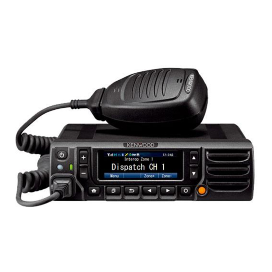
NX-5900 is a model that operation panel is attached.
NX-5900(B) is a model that operation panel is not attached.
The illustration is NX-5900.
COPYRIGHT © 2015 JVC KENWOOD Corporation
TABLE OF CONTENTS
Preliminary
This product uses Lead Free solder.
No.RA032<Rev.001>
2015/9
Advertisement
Table of Contents

Related Manuals for Kenwood NX-5900


Summary of Contents for Kenwood NX-5900
-
Page 1: Table Of Contents
9 S ERVICE MANUAL B5B-7211-00 NX-5900, NX-5900(B) NX-5900 is a model that operation panel is attached. NX-5900(B) is a model that operation panel is not attached. The illustration is NX-5900. COPYRIGHT © 2015 JVC KENWOOD Corporation TABLE OF CONTENTS PRECAUTION............... . . 1-4 SPECIFIC SERVICE INSTRUCTIONS . - Page 2 Neither is any liability assumed for damages resulting from the use of the information contained herein. JVC KENWOOD Corporation reserves the right to make changes to any products herein at any time for improvement purposes. Firmware Copyrights The title to and ownership of copyrights for firmware embedded in KENWOOD product memories are reserved for JVC KENWOOD Corporation.
- Page 3 4K00F1D, 4K00F7W, 4K00F2D Analog measurements made per TIA 603 and specifications shown are typical. P25 Digital measurements made per TIA 102CAAA and specifications shown are typical. JVC KENWOOD Corporation reserves the right to change specifications without prior notice or obligation. (No.RA032<Rev.001>)1-3...
-
Page 4: Precaution
NX-5900 Refer to the KRK-14H/15B service manual It's possible to combine and install the (B5B-7173-10) for Setup and installation RF Deck (NX-5900), Remote Kit (KRK-14H, Are you using information for all combinations. KRK-15B), Control Head (KCH-19, KCH-20R) the Multi-RF Deck/Multi-Control... - Page 5 ] + Power ON Select the “Panel Test” using the [ ] / [ ] key. Press the [ ] key. PC mode Received commands from PC Panel tuning mode [Panel test mode] + [ The illustration is NX-5900. KPG-46U/46X Transceiver Fig.1 (No.RA032<Rev.001>)1-5...
- Page 6 ] or [*] key, 2.2.6.3 Programming “CLONE MODE” displayed if the entered password is (1) Start up the firmware programming software (KENWOOD correct. If password is incorrect, “Input Password” is re- Firmware Loader). The KFL.exe exists in the KPG-D1/D1N displayed.
- Page 7 6.25kHz/12.5kHz • “Model name” must be same to clone the transceiver. P25: 12.5kHz 5 RX Signaling RX QT/DQT Receive QT/DQT The illustration is NX-5900. 6 TX Signaling TX QT/DQT Transmit QT/DQT 7 RX RAN RX RAN None, 1~63...
- Page 8 • Key operation Key\Item Zone Select Channel RX Frequency TX Frequency Channel Channel RX Signaling TX Signaling Select Type Spacing Decision Decision Decision Decision Decision Decision Decision Decision Unused Back to the Back to the pre- Back Back to the Back to the Back to the Back to the...
- Page 9 • Direct enter mode Key\Item Channel Frequency Frequency Signaling Signaling Name Decision Character/Channel name decision Delete Unused Exit panel program mode Unused Character selection (upper case char- acter → lower-case character → digit → upper case character...) Character selection (upper case char- acter →...
- Page 10 • Front panel programming mode flow chart NX-5900 Input Password Clone/Front Panel Password Enter the Front panel programming mode by using section "2.2.2 How to Enter Each Mode". Front panel Programming mode ] or [ ] or [ ] or [...
- Page 11 (4) To exit the transceiver information mode, turn the transceiver power OFF. Note: When the SCM board is not equipped to the transceiver, SCM Firmware Version and SCM Hardware Version are displayed as "-.-.-." INSTALLATION NX-5900 External View (No.RA032<Rev.001>)1-11...
- Page 12 NX-5900(B) External View (170) ATTENTION: When installing the option, please take measures to prevent static electricity. 2.3.1 Ignition Sense Cable (KCT-46: Option) The KCT-46 is an optional cable for enabling the ignition func- tion. The ignition function lets you turn the power to the transceiv- er on and off with the car ignition key.
- Page 13 2.3.2 Horn Alert/P.A. Relay Unit (KAP-2: Option) (7) Pass the 6-pin connector of the cable (E37-1113-25) The Horn alert (max. 2A drive), Public address and External through the chassis hole <5> and insert the bush into the speaker function are enabled by installing the KAP-2 in the trans- shassis hole.
- Page 14 2.3.3 External Speaker (Option) Connection Procedure Insert the crimp terminal into the Square plug supplied with the 2.3.3.1 KES-3 KAP-2. The KES-3 is an external speaker for the 3.5-mm-diameter speaker jack. Connection Procedure Connect the KES-3 to the 3.5-mm-diameter speaker jack on the rear of the transceiver.
- Page 15 (G1D-0006-XX) (G1D-0055-XX) (F3K-0004-XX) Note: Supplied accessories with * mark are not used for the NX-5900. 2.3.4.2 INSTALLING THE MODULE IN THE TRANSCEIVER (1) Remove the cabinet, top packing and shielding plate of the (5) Pull and remove the release paper while pressing down on transceiver.
- Page 16 2.3.5 Changing D-SUB 25-pin connector (4 pin, 5 pin) con- figuration 2.3.5.1 Change configuration of D-SUB 25-pin connector from AUXIO9 to CTS 4 pin The output (4 pin) of D-SUB 25-pin connector is configured at the AUXIO9 as the default value. Remove the R950 chip jumpers and solder the chip jumpers to $R952.
- Page 17 2.4.1 Overview The NX-5900 is a 700/800MHz Analog FM & Digital Mobile transceiver designed to operate in the frequency range of 763 to 775.99375MHz, 793 to 805.99375MHz (700M) and 806 to 825MHz, 851 to 870MHz (800M). The unit consists of a receiver, a trans- mitter, a phase-locked loop (PLL) frequency synthesizer, a digital control unit, and a power supply circuit.
- Page 18 2.4.4 Transmitter System 2.4.4.1 Audio Band Circuit The signal from microphone is amplified and converted to digital signal by IC902. IC902 includes AGC function. Digital signal is transferred to IC706 thru SSI. 2.4.4.2 Base Band Circuit The audio signal transferred from IC902 is processed at IC706. Voice signals of 300Hz or lower and frequencies of 3kHz or higher are cut off and an audio range 300Hz to 3kHz is extracted.
- Page 19 2.4.5.2 There are TX VCO and RX VCO. The TX VCO (Q102) generates the carrier for the transmitter. The oscillation frequency of the VCO is half of transmit frequency. VCO oscillation frequency range is 381.5 to 435MHz. The transmit frequency range is 763 to 870MHz. The RX VCO (Q104) generates the 1st local signal for the receiver.
- Page 20 2.4.6.5 The DSP circuit consists of a MPU/DSP (IC706) and processes the baseband signal. The DSP operates at 288MHz (MAX) clock, the I/O section operates at 3.3V/1.8V and the core section operates at 1.2V. The DSP carries out the following processes: •...
- Page 21 Final / Drive amp 31BU Q8, Q9, D11 50BU Power management IC 5V Reg 3.1V AVR 12BU MPU/DSP RTC 1.2V AVR SCTAM Q1, Q3 Option Board DC SW /BINT MPU/DSP Core 5.4V DC/DC 1.2V AVR MPU/DSP PLL BAT_CNT from Power management IC (IC2) MPU/DSP I/O(B), DDR IC11...
- Page 22 2.4.8 Signaling Circuit 2.4.8.1 Encode (QT/DQT/DTMF/2-tone/MSK) Each signaling data signal of QT, DQT, DTMF, 2-tone and MSK is generated by IC706, superposed on a modulation signal and output to TX VCO and PLL IC. 2.4.8.2 Decode (QT/DQT/DTMF/2-tone/MSK) The audio signal is removed from the FM detection signal sent to the IC706 and the resulting signal is decoded by IC706. 2.4.9 Bluetooth/GPS Circuit The main component of the Bluetooth/GPS circuit is Bluetooth / GPS IC (IC5) on MODULE unit.
- Page 23 COMPONENTS DESCRIPTION Ref.No Part Name Description 2.5.1 Main unit (XC1-1021-80) IC904 Logic control Ref.No Part Name Description IC905 Buffer AMP (BER CK/BER DT) Voltage regulator (31BU) IC906 Level shift Power management IC907 Analog switch Voltage regulator (12BU) IC908 Schmitt trigger Voltage regulator (33A) IC909 RS-232C driver...
- Page 24 VARI CAP DIODE VCO assist tune DC switch D115 DIODE Speed up D17, 18 Diode Overvoltage protection D117 Variable VCO assist tune 2.5.3 SUB (Display) unit (XC3-0020-20) (Only NX-5900) capacitance diode D300 Diode T/R switch Ref.No Part Name Description D304 Diode...
- Page 25 Ref.No Part Name Description Pin No. Name Function DC switch O 5.4V output Q3, 4 DIGI DC switch CN749 (to Sub (Display) unit CN6) TRANSISTOR NC (IGN) - No connection DIGI DC switch (Ignition sense input) TRANSISTOR - No connection D1, 2 Zener diode Overvoltage protection...
- Page 26 Pin No. Name Function Pin No. Name Function AFO+ O AF signal output plus TXD2 I Serial data input 2 AFO- O AF signal output minus AUXIO4 I/O AUX input/output 4 I MIC signal input AUXIO8 I/O AUX input/output 8 - MIC ground AUXIO5 I/O AUX input/output 5...
- Page 27 Pin No. Name Function Pin No. Name Function J901 (ACC. D-Sub 25-pin) GPS_PA_EN GPS receiver part switching signal input GPS_ANT_SW Enable signal for 33GPS RXD1 Ground TXD1 Ground AUXIO9 GPS_ALM O Antenna open/short detection GPS_PWR O Antenna power supply detec- tion 2.6.3 Sub (Display) unit (XC3-0020-20) AUXIO8...
- Page 28 Pin No. Name Function Pin No. Name Function DB17 I/O LCD driver data output D[5] I/O LCD driver data input CABC - No connection D[6] I/O LCD driver data input RESX O LCD driver reset signal D[7] I/O LCD driver data input O Interface mode select D[8] I/O LCD driver data input...
- Page 29 2.6.4 D-Sub 25-pin connector specification Rating and Condition Pin No. Pin Name Signal Type Parameter Unit RXD1 Digital Input Voltage Range Threshold Low Threshold High 1.60 2.45 Baud Rate 300k TXD1 Digital Voltage Swing (3kΩ Load) ±5 ±5.2 Baud Rate 300k AUXIO9 Digital...
- Page 30 Rating and Condition Pin No. Pin Name Signal Type Parameter Unit Power Voltage This parameter depends on Battery Voltage Supply Current AUXO2 Digital The type of this port is open collector. -500 AUXO1 Digital The type of this port is open collector. -500 Analog Output Level...
-
Page 31: Disassembly
SECTION 3 DISASSEMBLY Precautions for Disassembly 3.1.2 Removing the speaker hardware fixture (J2B-0023- 00) and holder (J1K-0019-00) 3.1.1 Main PCB (Main unit A/2) disassembly (1) Remove the speaker lead from the holder hook. <1> (1) Remove all screws and antenna terminals on the Main (2) Remove the speaker connector from the display unit con- PCB. - Page 32 Precautions for Reassembly 3.2.1 Main PCB (Main unit A/2) reassembly (1) With the Main PCB turned over, insert the flat cable from the D-sub PCB (Main unit B/2) into the connector (CN906) on the Main PCB. (2) Place the Main PCB at its original position as shown in Fig- ure 3.
- Page 33 Note: 3.2.6 Installing the holder (J1K-0019-00) and speaker hard- Push evenly on the top cover and be careful that you do ware fixture (J2B-0023-00) not bend it as you install it on the shield cover. (1) Insert two tabs of the holder (J1K-0019-00) into the hollows in the top of the panel.
-
Page 34: Adjustment
SECTION 4 ADJUSTMENT Controls 4.2.2 Key operation "Func" not appears on the sub LCD display Power switch Function Display Volume Up/Down key Channel Up/Down key Push: Volume up Hold: Volume up continu- ously Push: Volume down Hold: Volume down con- tinuously Push: Test channel up Channel No. - Page 35 "Func" appears on the sub LCD display "Func" appears on the sub LCD display Function Display Function Display Key/LCD check The contents of the [PTT] Transmit pressed key etc., [0] to [9] Function off appear. High power/Medium High: "H" [#], [ ] power/Low power Medium: "M"...
- Page 36 NXDN Mode signaling None Single Tone Encode (1000Hz) RAN1 RAN1 None MSK PN9 None MSK Decode MSK Encode RAN1 Maximum Deviation Pattern P25 Phase1 signaling FSW + PN9 FSW + PN9 Tone Pattern (1031Hz) Tone Pattern (1031Hz) NAC 293 NAC 293 RAN: Radio Access Number NAC 023 NAC 023...
- Page 37 4.3.2 Key operation RSSI Reference, Open Squelch, Low RSSI, High RSSI, Tight Squelch Function Tuning point Display RX (MHz) TX (MHz) Push Hold (1 second) 700M RX/TA 700M RX/TA 763.100000 763.000000 Volume up Continuation up Volume down Continuation down 700M RX/TA 700M RX/TA 769.100000 769.000000...
- Page 38 4.3.4 Adjustment item supplement Adjustment Item Description Adjustment Item Description DTMF Deviation DTMF tone deviation is adjusted. Receive Assist The lock voltage of VCO (Receive) is ad- justed. Single Tone Devia- The deviation of Single Tone used in “2- This item must be adjusted before all ad- tion tone”...
- Page 39 4.3.5 Adjustment item and Display Order Adjusutment Main Sub LCD Adjust item display (Analog (Analog (Analog (P25 (P25 (NXDN (NXDN item display Wide) Wide 4k) Narrow) Phase1) Phase2) Nar- Very Number row) Nar- row) Adjustment range Receive Assist RAST (CV voltage) Common 4 point ADJ Section 2...
- Page 40 Order Adjusutment Main Sub LCD Adjust item display (Analog (Analog (Analog (P25 (P25 (NXDN (NXDN item display Wide) Wide 4k) Narrow) Phase1) Phase2) Nar- Very Number row) Nar- row) Adjustment range LTR Deviation Transmitter Section 19 1~1024 DTMF Deviation DTMF Transmitter Section 20 1~1024...
- Page 41 4.3.6 Panel tuning mode flow chart Note: * In this Panel tuning mode flow chart, the Adjustment item name is modified. Adjustment Item N/W/VN Panel Test Mode LCD Display QT Deviation For all adjustment items, press the [ ] key DQT Deviation to write the adjustment value.
- Page 42 BER (Bit Error Rate) Measurement (For example, if the BER is 0.86%, the display shows (1) The Panel Test Mode is used to measure the BER (Refer "0.86".) "4.2.1 Test mode operation features"). (2) Select "10" (P25 Phase1), "7" (P25 Phase2) and "7" (NXDN Mode) for test signaling (Refer to "4.2.3 Frequency and Signaling"...
- Page 43 Test cable for microphone input (E30-3360-28) Tuning cable (E30-3383-05 or E30-7754-05) Adapter cable (E30-3383-05 or E30-7754-05) is required for GREEN injecting an audio if PC tuning is used. See “PC Mode” section for the connection. BLACK Illust is E30-3383-05. BLUE SHIELD MIC-E WHITE...
- Page 44 Item Condition Measurement Adjustment Specifica- tions Panel test PC test mode Test- Unit Terminal Unit Parts Method /Remarks mode equipment 2-2. 1)CH-Sig: 1-1 1)Test Channel Power Panel ANT Check 27.0W~30.0W High PTT: ON Channel: 1 meter 13.0A or less power TA: ON Test Signaling Mode: Analog Ammeter...
- Page 45 Item Condition Measurement Adjustment Specifica- tions Panel test PC test mode Test- Unit Terminal Unit Parts Method /Remarks mode equipment 3-1. 1)CH-Sig: 1-1 1)Test Channel Power Panel ANT Check 1.5W~2.0W PTT: ON Channel: 1 meter 5.0A or less power TA: OFF Test Signaling Mode: Analog Ammeter check...
- Page 46 Item Condition Measurement Adjustment Specifica- tions Panel test PC test mode Test- Unit Terminal Unit Parts Method /Remarks mode equipment 3-4. 1)CH-Sig: 7-1 1)Test Channel Power Panel ANT Check 1.5W~2.0W PTT: ON Channel: 7 meter 5.0A or less power TA: ON Test Signaling Mode: Analog Ammeter check...
- Page 47 Common Section Item Condition Measurement Adjustment Specifications /Remarks Panel tuning PC test mode Test- Unit Ter- Unit Parts Method mode equip- minal ment 1) DC voltage:13.6V Setting 2) SSG standard modulation [Wide 5k] MOD:1kHz,DEV:3kHz [Wide 4k] MOD:1kHz,DEV:2.4kHz [Narrow] MOD:1kHz,DEV:1.5kHz 1) Adj item: 1) Adj item: Panel [Panel [PC test mode]...
- Page 48 Item Condition Measurement Adjustment Specifications /Remarks Panel tuning PC test mode Test- Unit Ter- Unit Parts Method mode equip- minal ment *The Frequen- 1) Adj item: Panel ANT Panel [Panel [PC test mode] [PC test mode] Frequency cy adjust- [Frequency] tuning Press [Start] button of “IF20”...
- Page 49 Transmitter Section Item Condition Measurement Adjustment Specifica- tions Panel tuning PC test mode Test- Unit Ter- Unit Parts Method /Remarks mode equip- minal ment 1) Adj item: 1) Adj item: Power Panel ANT Panel [Panel [PC test mode] Ramp [RAMPU] [Ramp Up Offset] meter tuning...
- Page 50 Item Condition Measurement Adjustment Specifica- tions Panel tuning PC test mode Test- Unit Ter- Unit Parts Method /Remarks mode equip- minal ment 1) Adj item: 1) Adj item: Power Panel ANT Panel [Panel 45W (700M RX/TA Low, ±1.0W High [An MAX_H] [High Maximum meter tuning...
- Page 51 Item Condition Measurement Adjustment Specifica- tions Panel tuning PC test mode Test- Unit Ter- Unit Parts Method /Remarks mode equip- minal ment 1) Adj item: 1) Adj item: Power Panel ANT Panel [Panel 45W (700M RX/TA Low, ±1.0W [An MAX_L] [Low Maximum meter tuning...
- Page 52 Item Condition Measurement Adjustment Specifica- tions Panel tuning PC test mode Test- Unit Ter- Unit Parts Method /Remarks mode equip- minal ment 1) Adj item: 1) Adj item: Power Panel ANT Panel [Panel Write the value as Medium [An M_LMT] [Medium Transmit meter tuning...
- Page 53 Item Condition Measurement Adjustment Specifica- tions Panel tuning PC test mode Test- Unit Ter- Unit Parts Method /Remarks mode equip- minal ment 1) Adj item: 1) Adj item: Power Panel ANT Panel [Panel [7RL]: 28.5W ±1.0W High [An H_PWR] [High Transmit meter tuning [7RH]: 28.5W...
- Page 54 [TX High] ready. adjustment [700M TX [Frequency: (Same as TK-5910, the value after all High]→ 800MHz Band] old model of NX-5900). adjustment [800M TX Low]→ [TX Low]→ Press [AUX(Orange)] point was [800M TX [TX High]→ key to switch the tone to adjusted.
- Page 55 Item Condition Measurement Adjustment Specifica- tions Panel tuning PC test mode Test- Unit Ter- Unit Parts Method /Remarks mode equip- minal ment 1) Adj item: 1) Adj item: Devia- Panel ANT Panel [Panel Write fixed value for 4150~4250Hz Maxi- [Aw ADEV] [Maxmum tion tuning...
- Page 56 Item Condition Measurement Adjustment Specifica- tions Panel tuning PC test mode Test- Unit Ter- Unit Parts Method /Remarks mode equip- minal ment [Analog 1) Adj item: 1) Adj item: Devia- Panel ANT Panel [Panel Write fixed value for 2050~2150Hz Narrow] [As ADEV] [Maxmum tion...
- Page 57 Item Condition Measurement Adjustment Specifica- tions Panel tuning PC test mode Test- Unit Ter- Unit Parts Method /Remarks mode equip- minal ment 15. P25 1) Adj item: 1) Adj item: Devia- Panel ANT Panel [Panel Write fixed value for 3090~3215Hz H-CPM [P2 P2DEV] [P25 H-CPM...
- Page 58 Item Condition Measurement Adjustment Specifica- tions Panel tuning PC test mode Test- Unit Ter- Unit Parts Method /Remarks mode equip- minal ment [NXDN 1) Adj item: 1) Adj item: Devia- Panel ANT Panel [Panel Write fixed value for 1311~1363Hz Very [Nv NDEV] [NXDN High tion...
- Page 59 Item Condition Measurement Adjustment Specifica- tions Panel tuning PC test mode Test- Unit Ter- Unit Parts Method /Remarks mode equip- minal ment [Analog 1) Adj item: 1) Adj item: Devia- Panel ANT Panel [Panel Write the value as fol- 0.60kHz±0.05 Wide [An QT] [QT Deviation...
- Page 60 Item Condition Measurement Adjustment Specifica- tions Panel tuning PC test mode Test- Unit Ter- Unit Parts Method /Remarks mode equip- minal ment 18. DQT 1) Adj item: 1) Adj item: Devia- Panel ANT Panel [Panel Write the value as fol- 0.75kHz±0.05 Devia- [Aw DQT]...
- Page 61 Item Condition Measurement Adjustment Specifica- tions Panel tuning PC test mode Test- Unit Ter- Unit Parts Method /Remarks mode equip- minal ment [Analog 1) Adj item: 1) Adj item: Devia- Panel ANT Panel [Panel Write the value as fol- 0.35kHz±0.05 Narrow] [An DQT] [DQT Deviation...
- Page 62 Item Condition Measurement Adjustment Specifica- tions Panel tuning PC test mode Test- Unit Ter- Unit Parts Method /Remarks mode equip- minal ment [Analog 1) Adj item: 1) Adj item: Devia- Panel ANT Panel [Panel Write the value as fol- 0.9kHz±0.05k Wide [As LTR] [LTR Deviation...
- Page 63 Item Condition Measurement Adjustment Specifica- tions Panel tuning PC test mode Test- Unit Ter- Unit Parts Method /Remarks mode equip- minal ment 1) Adj item: 1) Adj item: Devia- Panel ANT Panel [Panel Write the value as fol- 2.50kHz±0.05 DTMF [Aw DTMF] [DTMF Deviation tion...
- Page 64 Item Condition Measurement Adjustment Specifica- tions Panel tuning PC test mode Test- Unit Ter- Unit Parts Method /Remarks mode equip- minal ment [Analog 1) Adj item: 1) Adj item: Devia- Panel ANT Panel [Panel Write the value as fol- 1.25kHz±0.05 Narrow] [An DTMF] [DTMF Deviation...
- Page 65 Item Condition Measurement Adjustment Specifica- tions Panel tuning PC test mode Test- Unit Ter- Unit Parts Method /Remarks mode equip- minal ment [Analog 1) Adj item: 1) Adj item: Devia- Panel ANT Panel [Panel Write the value as fol- 2.40kHz±0.05 Wide [As TONE] [Single Tone...
- Page 66 Item Condition Measurement Adjustment Specifica- tions Panel tuning PC test mode Test- Unit Ter- Unit Parts Method /Remarks mode equip- minal ment 22. MSK 1) Adj item: 1) Adj item: Devia- Panel ANT Panel [Panel Write the value as fol- 3.00kHz±0.05 Devia- [Aw MSK]...
- Page 67 Item Condition Measurement Adjustment Specifica- tions Panel tuning PC test mode Test- Unit Ter- Unit Parts Method /Remarks mode equip- minal ment [Analog 1) Adj item: 1) Adj item: Devia- Panel ANT Panel [Panel Write the value as fol- 1.50kHz±0.05 Narrow] [An MSK] [MSK Deviation...
- Page 68 4.9.1 Necessary Deviation adjustment item for each signaling and mode The following shows the necessary adjustment items for each signaling deviation. Please read the following table like the following example. In the case of the signaling "QT (Wide 5k)", this signaling is composed of three elements [Balance, Maximum Deviation (An- alog Wide 5k) and QT Deviation (Wide 5k)].
- Page 69 4.10 Receiver Section Item Condition Measurement Adjustment Specifi- cations Panel tuning mode PC test mode Test- Unit Ter- Unit Parts Method /Remarks equip- minal ment [Panel test mode] 1) Test Channel Panel ANT Panel [Panel Volume Up/Down knob to 1.41V AF level 1) CH-Sig: 1-1 Channel: 1...
- Page 70 Item Condition Measurement Adjustment Specifi- cations Panel tuning mode PC test mode Test- Unit Ter- Unit Parts Method /Remarks equip- minal ment [Analog 1) Adj item: 1) Adj item: Panel ANT Panel [Panel tuning mode] Wide [As SQL] [Open Squelch Distor- Ext.
- Page 71 Item Condition Measurement Adjustment Specifi- cations Panel tuning mode PC test mode Test- Unit Ter- Unit Parts Method /Remarks equip- minal ment [P25 1) Adj item: 1) Adj item: Panel ANT Panel [Panel tuning mode] (C4FM)] [P1 SQL] [Open Squelch Distor- Ext.
- Page 72 Item Condition Measurement Adjustment Specifi- cations Panel tuning mode PC test mode Test- Unit Ter- Unit Parts Method /Remarks equip- minal ment [NXDN 1) Adj item: 1) Adj item: Panel ANT Panel [Panel tuning mode] Narrow] [Nn SQL] [Open Squelch Distor- Ext.
- Page 73 Item Condition Measurement Adjustment Specifi- cations Panel tuning mode PC test mode Test- Unit Ter- Unit Parts Method /Remarks equip- minal ment 1) Adj item: 1) Adj item: Panel ANT Panel [Panel tuning mode] [An LRSSI] [Low RSSI (Analog Ext. After input signal from RSSI Adjust:[***]...
- Page 74 Item Condition Measurement Adjustment Specifi- cations Panel tuning mode PC test mode Test- Unit Ter- Unit Parts Method /Remarks equip- minal ment 1) Adj item: 1) Adj item: Panel ANT Panel [Panel tuning mode] Tight [Aw SQLT] [Tight Squelch Distor- Ext.
- Page 75 Item Condition Measurement Adjustment Specifi- cations Panel tuning mode PC test mode Test- Unit Ter- Unit Parts Method /Remarks equip- minal ment [Analog 1) Adj item: 1) Adj item: Panel ANT Panel [Panel tuning mode] Narrow] [As SQLT] [Tight Squelch Distor- Ext.
-
Page 76: Troubleshooting
SECTION 5 TROUBLESHOOTING Fault Diagnosis of the BGA (Ball Grid Array) IC Overview A flowchart for determining whether or not the transceiver can be powered on (the LCD does not function even if the power switch is turned on) due to broken BGA parts. BGA parts MPU/DSP (IC706), mobile DDR (IC702), Flash memory (IC701) When the BGA IC is problematic, please bring the printed circuit board (XC1-1021-81) in for service. - Page 77 Checking the output signal from the MPU/DSP. Checking the control signal output from If the /FRST is always 0V, the MPU/DSP When an abnormal the MPU/DSP is broken. value is confirmed. Points to be checked Normal voltage Remove D701 to check the voltage of Flash memory side R732.
- Page 78 *1 If 12M, 18M or 33M has still abnormal voltage after the implementation of each procedure above, 54M(IC8), 12M(A1), 18M(IC11), 33M(IC5) or one of these peripheral circuit is broken. 54M (normally 5.4V at L12) has an abnormal voltage, check the MSP430G25KGCA (IC2) according to the following procedure. Checking the operation of the IC2 When VIN of 54M Check that the voltage of VN of 54M (IC8-2pin)
- Page 79 Checking the operation of IC2 (/PSW and /IGN) Check that the signal /PSW (IC2-10pin) and /PSW_OUT (IC2-15pin) are linked with the power button on KCH-19 in power on state. Check that the signal /PSW and /PSW_OUT are IC2 is broken. 0V during the power button is pressed.
- Page 80 Failure diagnosis of the GPS section Over view: When the GPS function does not operate, use this flowchart to determine the problem. Major parts for a GPS circuit IC706 GPS antenna (KRA-40 (option)) UART UART UART GPS antenna unit Level Coaxial cable (E0E-0003-00) conversion SAW Filter (L9)
- Page 81 Check the Module (BT/GPS) unit PCB side B. When an abnormal When a normal Verify the power supply voltage Verify the BT/GPS power condition is confirmed. condition is confirmed. [The KRA-40 may be broken] after removing the KRA-40. supply. Replace the KRA-40. (33GPS) L6: 3.3V (33GPS) L6: 3.3V When an abnormal...
- Page 82 Check the Main unit P CB. Verify the BT/GPS control Verify the BT/GPS control When an abnormal When an abnormal signal (G_TXD2). signal (TXD2). condition is confirmed. condition is confirmed. [The MPU/DSP IC is abnormal] CP705 (2 pin): CN735 (15 pin): Square waveform Replace the PCB.
- Page 83 Failure diagnosis of the Bluetooth section Over view: When the Bluetooth function does not operate, use this flowchart to determine the problem. Major parts for a Bluetooth circuit IC706 Bluetooth antenna (Pattern Antenna) UART UART UART LC filter (L11) Level Bluetooth/GPS (IC5) conversion Bluet oot h...
- Page 84 When a normal condition is confirmed. Verify the reference clock for the [The reference clock circuit When an abnormal BT/GPS. for the BT/GPS is faulty] condition is confirmed. (BT_CLK) Intersection of Visual check of the R9, Q1, R10, R26, R12, R13, C8 and C9: Sine waveform, X1, C4, C8, C9 (Whether not damaged) Replace any abnormal parts.
- Page 85 When a normal condition is confirmed. When an abnormal When an abnormal Verify the BT/GPS control Verify the BT/GPS control condition is confirmed. condition is confirmed. signal (18BT_HCI_TX.). signal (RXD2). Check the Main unit PCB (c). IC6 (18 pin): CN1 (7 pin): Square waveform Square waveform UART data UART data of 3.3V logic.
- Page 86 Number Firmware NX-5900 Firmware. NX-5900 (F,K) XC1-1021-80 XC1-1021-81 FPU Data XC1-102 (NX-5900) F type data. (PC programming mode) Method of confirming “Original Main unit” and “Service Various Adjustment Data General adjustment values for the Main unit” (PC Test mode) XC1-102 (NX-5900) .
- Page 87 Note: • When a new printed circuit board is used, the KENWOOD • When using the ESN Validation function of NXDN Trunk- ESN changes, as does the Transceiver Information dis- ing, the NXDN ESN number changes when the circuit play of the KPG-D1/D1N, but this does not have any effect board is changed (the number is written on the circuit on the operation of the transceiver.
- Page 88 MEMO...
- Page 89 SCHEMATIC DIAGRAM MAIN UNIT (XC1-1021-80 (NX-5900(K), NX-5900B(F), NX-5900B(K))) NX-5900 700/800MHz THP1 IC13,D15 IC300 MAIN UNIT(A/2)(XC1-102) DC-DC BGU6104 4.92V 19.72V 19.72V R:0V PRE-DRIVE AMP C324 CONVERTER(200C) PRE-DRIVE AMP R:0V DB2J40700 200C T:4.98V BUFFER AMP DOUBLER AMP CUR_ADJ Q300 T:2.23V(H) RD01MUS2-T113 2.23V(L) L301 1.72V...
- Page 90 BLOCK DIAGRAM MAIN UNIT Main Unit (XC1-102 A/2) IC706 700MHz:763~775.99375MHz(RX/TX) IC702 DDR_A[0]~DDR_A[13] :793~805.99375MHz(TX) DDR_BA[0],DDR_BA[1] 800MHz:806~825MHz(TX) DDR_CAS,DDR_CKE,DDR_CLKN :851~870MHz(RX/TX) DDR_CLKP,DDR_CS DDR_DQM[0],DDR_DQM[1] IC100 Q102 SKY72310362LF MCH3914-H/8/ DDR_RAS,DDR_WE VCO_MOD D110 DDR_DQS[0],DDR_DQS[1] SMV1801-079LF DDR_D[0]~DDR_D[15] D106 D305 L8104 SMV1705-079LF D306 L8104 IC101 IC701 D107,108,109,117 D308 L8104 TC7SH17FUF SMV1130-079LF Q105...
- Page 91 SUB (Display) UNIT Sub (Display) Unit (XC3-002) DAT[0]~DAT[15] ADD[23] LCDRST BU30TD2WNVX MM3404A50URE 30LCD VOLTAGE REGULATOR VOLTAGE REGULATOR KEYi3(KEYi3_2) KEYi2(KEYi2_2) /PSW KEYi1(KEYi1_2) BH1721FVC KEYi0(KEYi0_2) LIGHT IC10 SENSOR TC35894FG I2CCK Q2 (1/2) I2CDT /EMG SSM6N37FE KEYo2 KEYo1 Q2(2/2) SSM6N37FE KEYo0 To LCD LCDRST KEYBLC LED_R...
-
Page 92: Printed Circuit Board
PRINTED CIRCUIT BOARD MAIN UNIT (XC1-1021-80) (XC1-1021-80 (NX-5900(K), NX-5900B(F), NX-5900B(K))) --- Component side view (J7C-0126-00) --- IC18 R402 CN909 CN908 CN19 C967 IC911 CN307 CN308 C423 D912 D911 D910 IC15 C399 L320 D915 D914 D913 TH306 F900 D918 R945 C943... - Page 93 MAIN UNIT (XC1-1021-80) (XC1-1021-80 (NX-5900(K), NX-5900B(F), NX-5900B(K))) --- Foil side view (J7C-0126-00) --- D924 Q906 C420 D905 R958 C977 R960 Q303 D307 C396 C349 R329 C395 C394 C355 R933 R930 C937 R338 R938 R963 R361 C986 C419 C418 R964 F300...
- Page 94 A-1C ADDRESS TABLE OF BOARD PARTS Y axis Side Each address may have an address error by one X axis interval. REF.NO. LOCATION REF.NO. LOCATION REF.NO. LOCATION REF.NO. LOCATION REF.NO. LOCATION REF.NO. LOCATION REF.NO. LOCATION REF.NO. LOCATION REF.NO. LOCATION REF.NO. LOCATION REF.NO. LOCATION REF.NO. LOCATION REF.NO. LOCATION REF.NO. LOCATION REF.NO. LOCATION REF.NO. LOCATION REF.NO. LOCATION Q305 A- 3B D909...
- Page 95 MODULE (BT/GPS) UNIT (XC2-0031-80) --- Component side view (J7C-0037-00) --- --- Foil side view (J7C-0037-00) --- XC2-003/004 J7C-0037 A-1C ADDRESS TABLE OF BOARD PARTS Side Y axis Each address may have an address error by one interval. X axis REF.NO. LOCATION REF.NO. LOCATION REF.NO. LOCATION REF.NO. LOCATION REF.NO. LOCATION REF.NO. LOCATION B- 3A CAPACITOR A- 2B...
- Page 96 SUB (DISPLAY) UNIT (XC3-0020-20 (NX-5900(K))) --- Component side view (J7C-0038-00) --- ADDRESS TABLE OF BOARD PARTS Each address may have an address error by one interval. A-1C Side Y axis X axis REF.NO. LOCATION REF.NO. LOCATION REF.NO. LOCATION B- 5A...
- Page 97 MODULE (BT/GPS) UNIT (XC2-0031-80) BT ANT MODULE UNIT (BT/GPS)(XC2-0031-80) LEVEL CONVERTER 1.8V 1.8V F10-3226-05 1.80V 18BT_HCI_TX 18BT_TX 74AVC4TD245GU 18BT_HCI_RX 18BT_RX VOLTAGE VOLTAGE REGULATOR(18BT) REGULATOR(33BT) DIR4 DIR1 3.31V 0.1u VCC(A) EM6M2 VCC(B) 0.1u 19.2MHz DIR3 DIR2 VCoNT VCC 4 DC SW LEVEL CONVERTER MSL-SL-MSL...
- Page 98 SUB (DISPLAY) UNIT (XC3-0020-20 (NX-5900(K))) SUB UNIT (DISPLAY)(XC3-002) KEYi3_2 B30-2364-05 S70-0901-05 S70-0901-05 S70-0901-05 THREE COLOR 3.28V 13.60V B30-2365-05 B30-2365-05 B30-2365-05 VSSA /KEYINT VSSA KEYi2_2 S70-0901-05 S70-0901-05 S70-0901-05 Q3,Q4,Q6 VSSA LTC014EEBFS8 0.1u 2.99V LED_B VSSD 5.32V B30-2365-05 B30-2365-05 B30-2365-05 VSSD KPY11...
-
Page 99: Interconnection Diagram
INTERCONNECTION DIAGRAM IC911 AF AMP LA4425A 20pin Option NX-5900 (K) only R402 CN749 INT SP NC(IGN) NC(IGN) CN907 CN906 A U X I O 6 A U X I O 6 A U X I O 7 A U X I O 7... -
Page 100: Level Diagram
LEVEL DIAGRAM Receiver Section 1st IF (58.05MHz) AF (1kHz) RF (Center Frequency) -120dBm -123dBm -124dBm -113dBm -114dBm -116dBm -117dBm -111dBm 141mVrms -121dBm -114dBm -102dBm 116mVrms D305 C552 L521 C544 Q501 C534 L510 C517 IC502 D306 IC501 IC600 IC706 IC902 IC719 C413 D308 C533 IC500 C500 XF600 C663 Q604 C658 Q603 C637 C927 IC903... -
Page 101: Parts List
PARTS LIST [NX-5900,NX-5900(B)] * SAFETY PRECAUTION Parts identified by the symbol are critical for safety. Replace only with specified part numbers. * BEWARE OF BOGUS PARTS Parts that do not meet specifications may cause trouble in regard to safety and performance. - Page 102 Exploded view of general assembly and parts list Block No.M1MM MAIN UNIT<01> SUB (DISPLAY) UNIT<03> MODULE (BT/GPS) UNIT<02> 3-2(No.RA032<Rev.001>)
- Page 103 General assembly Block No. [M][1][M][M] Symbol No. Part No. Part Name Description Local A0C-0107-00 PLASTIC CABINET A6C-0003-20 PANEL ASSY 5900_K B09-0681-03 CAP(KAP-2) B09-0754-05 CAP(SMA) B0K-0004-00 CAP(D-SUB) B1B-0017-00 ILLUMINATION GUIDE 5900_K B38-0966-05 LCD ASSY 5900_K B4B-0008-00 CAUTION STICKER 5900_K B4D-0021-00 BADGE 5900_K E04-0170-35 RF COAXIAL RECEPTACLE-N (ANT)
-
Page 104: Electrical Parts List
Electrical parts list MAIN UNIT Symbol No. Part No. Part Name Description Local XC1-1021-80 LTC014EEBFS8 DIGI TRANSISTOR *Note : This part cannot be replaced. There- EM6M2 fore, this part is not supplied as a service part. EM6M2 LTC014EEBFS8 DIGI TRANSISTOR Block No. - Page 105 Symbol No. Part No. Part Name Description Local Symbol No. Part No. Part Name Description Local D113 SMV1130-079LF VARIABLE CAPACITANCE DIODE CK73HBB1H471K C CAPACITOR 470PF K D114 SMV1130-079LF VARIABLE CAPACITANCE DIODE CK73GB1H105K C CAPACITOR 1.0UF K D115 1SS400SM DIODE CK73FB1C106K C CAPACITOR 10.0UF K D117...
- Page 106 Symbol No. Part No. Part Name Description Local Symbol No. Part No. Part Name Description Local C144 CC73HCH1HR75B C CAPACITOR 0.75PF B C322 CC73HCH1H470G C CAPACITOR 47PF G C145 CC73HCH1H0R5B C CAPACITOR 0.5PF B C323 CC73HCH1H470G C CAPACITOR 47PF G C146 CC73HCH1H060B C CAPACITOR 6.0PF B...
- Page 107 Symbol No. Part No. Part Name Description Local Symbol No. Part No. Part Name Description Local C438 CK73HB1H103K C CAPACITOR 10000PF K C616 CC73HCH1H330G C CAPACITOR 33PF G C439 CK73HBB1H332K C CAPACITOR 3300PF K C617 CC73HCH1H330G C CAPACITOR 33PF G C440 CK73HB1E333K C CAPACITOR...
- Page 108 Symbol No. Part No. Part Name Description Local Symbol No. Part No. Part Name Description Local C726 C93-1953-05 C CAPACITOR 0.10UF B C814 CC73HCH1H101J C CAPACITOR 100PF J C728 CK73GB0J106K C CAPACITOR 10.0UF K C815 CC73HCH1H101J C CAPACITOR 100PF J C729 CK73HB1H103K C CAPACITOR...
- Page 109 Symbol No. Part No. Part Name Description Local Symbol No. Part No. Part Name Description Local C956 CC73HCH1H101J C CAPACITOR 100PF J RK73JB1H102J MG RESISTOR 1.0K J 1/20W C957 CC73HCH1H101J C CAPACITOR 100PF J RK73HH1J103D MG RESISTOR 10K D 1/16W C958 CC73HCH1H101J C CAPACITOR 100PF J...
- Page 110 Symbol No. Part No. Part Name Description Local Symbol No. Part No. Part Name Description Local R145 RK73HH1J332D MG RESISTOR 3.3K D 1/16W R355 RK73HB1J271J MG RESISTOR 270 J 1/16W R146 RK73HB1J101J MG RESISTOR 100 J 1/16W R359 RK73GB2A000J MG RESISTOR 0.0 J 1/10W R147 RK73HB1J221J...
- Page 111 Symbol No. Part No. Part Name Description Local Symbol No. Part No. Part Name Description Local R520 RK73HH1J223D MG RESISTOR 22K D 1/16W R742 RK73HB1J102J MG RESISTOR 1.0K J 1/16W R521 RK73HH1J223D MG RESISTOR 22K D 1/16W R744 RK73HB1J102J MG RESISTOR 1.0K J 1/16W R527 RK73HB1J000J...
- Page 112 Symbol No. Part No. Part Name Description Local Symbol No. Part No. Part Name Description Local R858 RK73HH1J223D MG RESISTOR 22K D 1/16W R966 RK73HB1J471J MG RESISTOR 470 J 1/16W R859 RK73HH1J223D MG RESISTOR 22K D 1/16W R967 RK73GB2A221J MG RESISTOR 220 J 1/10W R862 RK73HB1J222J...
- Page 113 Symbol No. Part No. Part Name Description Local Symbol No. Part No. Part Name Description Local L142 LK73G0AFR27J M.CHIP INDUCTOR 270NH L701 LB73H0AV-003 CHIP FERRITE BEADS L300 L40-3363-71 SMALL FIXED INDUCTOR 3.3NH L702 LB73G0AK-001 CHIP FERRITE BEADS L301 LK73H0AM33NJ M.CHIP INDUCTOR 33NH L711 LR77Z0AE4R7J...
- Page 114 Symbol No. Part No. Part Name Description Local Symbol No. Part No. Part Name Description Local XF600 L7B-0001-00 RK73HB1J101J MG RESISTOR 100 J 1/16W RK73HB1J103J MG RESISTOR 10K J 1/16W RK73HB1J103J MG RESISTOR 10K J 1/16W RK73HB1J101J MG RESISTOR 100 J 1/16W MODULE (BT/GPS) UNIT RK73HB1J101J MG RESISTOR...
- Page 115 Symbol No. Part No. Part Name Description Local Symbol No. Part No. Part Name Description Local B30-2365-05 WHITE RK73HB1J000J MG RESISTOR 0.0 J 1/16W B30-2365-05 WHITE RK73HB1J000J MG RESISTOR 0.0 J 1/16W B30-2365-05 WHITE RK73HB1J000J MG RESISTOR 0.0 J 1/16W B30-2365-05 WHITE RK73HB1J000J...
- Page 116 Symbol No. Part No. Part Name Description Local S70-0901-05 TACT SWITCH S70-0901-05 TACT SWITCH S70-0901-05 TACT SWITCH S70-0901-05 TACT SWITCH S70-0901-05 TACT SWITCH S70-0901-05 TACT SWITCH S70-0901-05 TACT SWITCH 3-16(No.RA032<Rev.001>)
- Page 117 Packing materials and accessories parts list (NX-5900_K) Block No.M2MM Packing and accessories Block No. [M][2][M][M] Symbol No. Part No. Part Name Description Local B5A-0868-00 INSTRUCTION MANUAL ------------ PAMPHLET ------------ PAMPHLET E30-7523-65 DC CORD ASSY F52-0024-05 FUSE(BLADE TYPE) 15A(x2) H0C-0007-00 INNER CARTON CASE H1C-0077-00 PACKING FIXTURE(LOWER) H1C-0078-00...
- Page 118 Packing materials and accessories parts list (NX-5900B_F,NX-5900B_K) Block No.M3MM Packing and accessories Block No. [M][3][M][M] Symbol No. Part No. Part Name Description Local B5A-0868-00 INSTRUCTION MANUAL ------------ PAMPHLET ------------ PAMPHLET H1C-0077-00 PACKING FIXTURE(LOWER) H1C-0078-00 PACKING FIXTURE(UPPER) H1C-0027-00 PACKING FIXTURE(SPACER) ------------ ANTI-STATIC BAG H5A-0617-00 ITEM CARTON...
- Page 119 MEMO...
- Page 120 JVC KENWOOD Corporation Communications Systems Business Unit (No.RA032<Rev.001>) Printed in Japan...
Need help?
Do you have a question about the NX-5900 and is the answer not in the manual?
Questions and answers