Advertisement
Quick Links
B5B-7316-00
RA073<Rev.001>
3 S ERVICE MANUAL
2019
COPYRIGHT © 2019 JVC KENWOOD Corporation
1
PRECAUTION. . . . . . . . . . . . . . . . . . . . . . . . . . . . . . . . . . . . . . . . . . . . . . . . . . . . . . . . . . . . . . . . . . . . . . . . . 1-4
2
SPECIFIC SERVICE INSTRUCTIONS . . . . . . . . . . . . . . . . . . . . . . . . . . . . . . . . . . . . . . . . . . . . . . . . . . . . . . 1-4
3
DISASSEMBLY . . . . . . . . . . . . . . . . . . . . . . . . . . . . . . . . . . . . . . . . . . . . . . . . . . . . . . . . . . . . . . . . . . . . . . 1-33
4
ADJUSTMENT . . . . . . . . . . . . . . . . . . . . . . . . . . . . . . . . . . . . . . . . . . . . . . . . . . . . . . . . . . . . . . . . . . . . . . . 1-36
5
TROUBLESHOOTING . . . . . . . . . . . . . . . . . . . . . . . . . . . . . . . . . . . . . . . . . . . . . . . . . . . . . . . . . . . . . . . . . 1-62
This product complies with the RoHS directive for the European market.
B5B-7316-00
SERVICE MANUAL
VHF DIGITAL TRANSCEIVER
NX-5700HB
COPYRIGHT © 2019 JVC KENWOOD Corporation
TABLE OF CONTENTS
This product uses Lead Free solder.
No.RA073<Rev.001>
2019/3
Advertisement

Related Manuals for Kenwood NX-5700HB


Summary of Contents for Kenwood NX-5700HB
-
Page 1: Table Of Contents
B5B-7316-00 NX-5700HB COPYRIGHT © 2019 JVC KENWOOD Corporation TABLE OF CONTENTS PRECAUTION............... . . 1-4 SPECIFIC SERVICE INSTRUCTIONS . - Page 2 Neither is any liability assumed for damages resulting from the use of the information contained herein. JVC KENWOOD Corporation reserves the right to make changes to any products herein at any time for improvement purposes. Firmware Copyrights The title to and ownership of copyrights for firmware embedded in KENWOOD product memories are reserved for JVC KENWOOD Corporation.
- Page 3 *1 25 and 30 kHz are not included in the models sold in the USA or US territories. P25 Digital measurements made per TIA 102CAAA, analog measurements made per TIA 603 and specifications shown are typical. JVC KENWOOD Corporation reserves the right to change specifications without prior notice or obligation. (No.RA073<Rev.001>)1-3...
-
Page 4: Precaution
110W NX-5700HB is complete by combining options with only the transceiver body (without panel). RF Deck (NX-5700HB) is possible to combine and install the Remote Kit (KRK-14H), Control Head (KCH-19, KCH-20R, KCH-21R) and Cable (KCT-71, KCT-72) respectively. Are you using the Multi-RF Deck/Multi-Control... - Page 5 REALIGNMENT Mode Operation 2.2.1 Modes Firmware programming • [AUX (Orange)] + Power ON mode*2 • [ ] + Power ON User mode Select the “Firmware Prog” using the [] / [] key. Panel tuning mode Panel test mode Press the [ ] key.
- Page 6 Note: 2.2.6.3 Programming The data stored in the PC must match the “Model Name” (1) Start up the firmware programming software (KENWOOD when it is written into the flash memory. Firmware Loader). The KFL.exe exists in the KPG-D1/D1N installed folder.
- Page 7 • Tuning data • Embedded message with password • ESN (Electronic Serial Number) data Key guide on the Clone/ Front Panel Programming Password input screen. NX-5700HB with • Confirm ([ ] key): The password confirmation KCH-20R • Delete ([ ] key): Delete the latest digit from the current...
- Page 8 Setup item Display Remarks Setup item Display Remarks 8 RX RAN RX RAN None, 1~63 1 RX Frequency RX Frequency Receive Frequency 9 TX RAN TX RAN None, 1~63 2 TX Frequency TX Frequency Transmit Frequency 10 RX NAC RX NAC 000~FFF 3 Channel Type Channel Type...
- Page 9 Key operation (2/3) TX Signaling RX RAN TX RAN RX NAC TX NAC TG ID List No. Transmit \Item Power Decision Decision Decision Decision Decision Decision Decision Back to the Back to the Back to the Back to the Back to the Back to the Back to the...
- Page 10 • Front panel programming mode flow chart Input Password Enter the Front panel programming mode by using section "2.2.2 How to Enter Each Mode". Clone/Front Panel Password Front panel Programming mode ] or [ Zone Select Keep This Change? Channel Select Channel Name ] or [ ] or [...
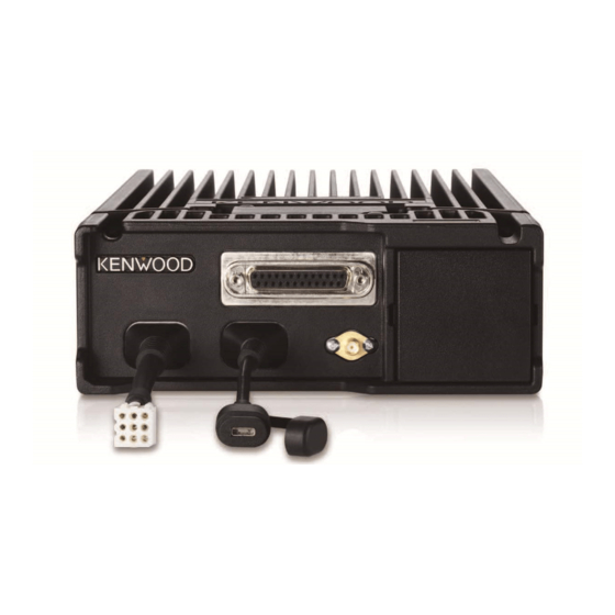
- Page 11 INSTALLATION External View 2-M x0.7 DEPTH OF DC CONNECTOR EFFECTIVE ANTENNA WITH CABLE THREAD:10 CONNECTOR (M TYPE) 3-M x0.7 DEPTH OF 3-M x0.7 EFFECTIVE DEPTH OF THREAD:8 EFFECTIVE THREAD:8 CAUTION LABEL (HOT SURFACE) KCT-71 CONNECTION CAUTION LABEL MODEL NAME PLATE (FCC) D-SUB CONNECTOR (25P) ACC.CONNECTOR...
- Page 12 For the multi RF Deck system, refer to the the KRK-14H/KRK-15B service manual (B5B-7173-20). Because the NX-5700HB has the function of the KRK-15B, it can be connected directly to the REMOTE CONTROL HEAD. The KRK-14H interface kit is required to connect the KCH-19 and radio. Refer to the KRK-14H/KRK-15B service manual (B5B- 7173-20).
- Page 13 2.3.1.1 Connecting procedure of the REMOTE CONTROL (3) Form the cable of the KCT-71 so as not to protrude from CABLE for Single Head system the groove of the chassis as shown below. (The procedure for connecting the KCT-71 to the radio and the procedure for connecting the KCT-77 to the radio are the same.) (1) Insert the connector of the KCT-71 into the connector of the radio.
- Page 14 2.3.1.2 Connecting procedure of the REMOTE CONTROL (4) Insert each of the 2 connectors of the KCT-71 made in step CABLE for Dual Head system (3) into the connectors of the radio. (The procedure for connecting the KCT-71 to the radio and the procedure for connecting the KCT-77 to the radio are the same.) (1) Cut the waterproof packing of the KCT-71 along the dotted line with a cutting tool so as to make the hole for the...
- Page 15 (1) Insert the KCT-18 lead terminal into pin 1 (IGN) of the (4) Insert the KCT-18 lead terminal into pin 1 (IGN) of the Socket (9-pin) NX-5700HB accessory. socket (12-pin) KCT-72 accessory. (2) Connect the socket (9-pin) to the connector (9-pin) for Socket (12-pin) KCT-72 accessory accessory on the front of the radio.
- Page 16 (1) The external speaker output from the connector (9-pin) for and 8. accessory on the front of the NX-5700HB is 12 W / 4 ohm. (1) Connect the lead wire of the KES-5 to the Socket (9-pin) (2) The KCH-20R Remote Control Head does not have a built- NX-5700HB accessory.
- Page 17 (G1D-0006-XX) (G1D-0055-XX) (F3K-0004-XX) Note: Supplied accessories with * mark are not used for the NX-5700HB. 2.3.5.2 INSTALLING THE MODULE IN THE TRANSCEIVER (1) Remove the M.CABINET and RUBBER SEAL of the (4) Insert the connector of the module into the CN5 of the Main transceiver.
- Page 18 (6) Reinstall the M.CABINET and RUBBER SEAL of the 2.3.6.2 Change configuration of D-SUB 25-pin connector transceiver. from DI to RTS Note: 5 pin • When the KWD-AE30/ KWD-AE31 is installed, select The input (5 pin) of D-SUB 25-pin connector is configured at the “Secure Cryptographic Module”...
- Page 19 2.4.1 Overview The NX-5700HB is a VHF Analog FM & Digital Mobile transceiver designed to operate in the frequency range of 136 to 174MHz. The unit consists of a receiver, a transmitter, a phase-locked loop (PLL) frequency synthesizer, a digital control unit, and a power supply circuit.
- Page 20 2.4.4 Transmitter System 2.4.4.1 Audio Band Circuit Refer to the “LEVEL DIAGRAM” in this manual. The signal from microphone is amplified and converted to digital signal by CODEC (IC902). IC902 includes AGC function. Digital signal is transferred to MPU/DSP (IC706) through SSI. 2.4.4.2 Baseband Circuit Refer to the "LEVEL DIAGRAM"...
- Page 21 2.4.5 PLL Frequency Synthesizer 2.4.5.1 TCXO (X700) TCXO (X700) generates a reference frequency of 19.2MHz for the PLL frequency synthesizer. This reference signal is buffered by Q700 and IC703. And it is distributed to PLL (IC100), IF IC (IC600), and MPU/DSP (IC706). The frequency adjustment is achieved by adjusting a D/A converter (IC715) output in the voltage of the control terminal of TCXO.
- Page 22 2.4.6.3 Interface Circuit The Interface unit is connected by a flexible cable (CN7 of the Main unit, CN1 of the Interface unit). Up to 2 control heads can be connected to the Interface unit. The control head is used for control and display of the radio equipment. 2.4.6.4 The DSP circuit consists of a MPU/DSP (IC706) and processes the base band signal.
- Page 23 RF Power Module 31BU Q8, Q9, D11 50BU Power management IC 5V Reg 3.1V AVR 12BU MPU/DSP RTC 1.2V AVR SCTAM1 Q1, Q3 Option Board DC SW /TAM_CNT MPU/DSP Core IC24 5.4V DC/DC 1.2V DC/DC MPU/DSP PLL BAT_CNT from Power management IC MPU/DSP I/O(B), DDR IC11 (IC2)
- Page 24 2.4.9 Bluetooth/GPS Circuit The main component of the Bluetooth/GPS circuit is Bluetooth / GPS IC (IC5) on Module (BT/GPS) unit. The clocks of Bluetooth/GPS IC require 19.2MHz for core and 32.768kHz slow clock (X1 and X2) for UART. Bluetooth/GPS IC communicates to the MPU/DSP (IC706) on the HCI UART. Interface of UART & Digital audio (PCM) between the MPU/DSP (IC706) and the Bluetooth/GPS IC (IC5), have level conversion at the level shift IC (IC6 and IC7) on Module (BT/GPS) unit.
- Page 25 COMPONENTS DESCRIPTION Ref.No. Part Name Use / Function 2.5.1 Main Unit (XC1-287F-00) IC903 AF amplifier (EXSP/DSUB) Ref.No. Part Name Use / Function IC904 Logic control Voltage regulator (31BU) IC905 Buffer amplifier (BER CK/BER DT) Power management IC906 Buffer amplifier Voltage regulator (12BU) IC907 Analog switch Voltage regulator (33A)
- Page 26 Ref.No. Part Name Use / Function Ref.No. Part Name Use / Function Q600 VCO oscillation D510 Variable RX Band-pass filter tune capacitance diode Q601 Transistor DC switch D600,601 Variable VCO frequency control Q602 Transistor Ripple filter capacitance diode Q603 Transistor IF amplifier D602 Diode...
- Page 27 TERMINAL FUNCTION Pin No. Name Function 2.6.1 Main unit (XC1-287F-00) - No connection Pin No. Name Function - No connection CN5 (for production) - No connection 1~20 - - No connection CN6 (to Module (BT/GPS) unit CN1) - No connection GPS_PWR I Antenna power supply detection - No connection...
- Page 28 Pin No. Name Function Pin No. Name Function AUXIO5 I/O AUX input/output 5 25pin ACCESSORY CONNECTOR - Ground - Refer to “D-sub 25pin connector specification”. AUXIO4 I/O AUX input/output 4 RXD0 AUXIO8 I/O AUX input/output 8 TXD0 AUXIO3 I/O AUX input/output 3 AUXIO9 TXD2 O Serial data output 2...
- Page 29 Pin No. Name Function Pin No. Name Function CTS2 O Serial data output - No connection RTS2 I Serial data input - No connection BT_AUD_DO I Audio signal input - No connection BT_AUD_DI O Audio signal output - No connection BCLK I Audio serial data bus bit clock - No connection...
- Page 30 2.6.4 D-Sub 25pin connector specification Pin Name Signal Type Rating and Condition Parameter Unit RXD0 Digital Input Voltage Range Threshold Low Threshold High 1.60 2.45 Baud Rate 300k TXD0 O Digital Voltage Swing (3kohm Load) ±5 ±5.2 Baud Rate 300k AUXIO9 I/O Digital -0.5...
- Page 31 Pin Name Signal Type Rating and Condition Parameter Unit AUXO1 O Digital The type of this port is open collector. -500 O Analog Output Level Vp-p Coupling Capacitor Allowable Load kohm Allowable Frequency 3000 O Analog Output Level 0.28 Vp-p Coupling Capacitor Allowable Load kohm...
- Page 32 2.6.5 Molex 9pin connector specification Pin Name Signal Type Rating and Condition Parameter Unit Analog Voltage Range O Analog Audio Output (3% Distortion) Allowable Frequency 3000 Analog Input Voltage 16.0 Input Current O Analog Output Voltage This parameter depends on HR1 Voltage. Output Voltage Loss Input Current O Analog...
-
Page 33: Disassembly
SECTION 3 DISASSEMBLY Precautions for Disassembly 3.1.2 Removing the Main unit (1) Disconnect the connectors of the Main unit. Note 2 3.1.1 Removing the M.CABINET, RUBBER SEAL and (2) Remove the solder fixing the antenna. SHIELDING COVER (3) Remove the FLAT SPRING. (1) Remove 6 screws fixing the M.CABINET(bottom).<1>... - Page 34 (6) The Main unit and the Interface unit are connected by FFC. Precautions for Reassembly When removing the Main unit, be careful not to apply 3.2.1 Wire forming excessive force to the FFC and the connectors. Refer to the following pictures. Main unit Interface unit 3.1.3 Removing the MOLDING COVER...
- Page 35 3.2.2 Attaching the RUBBER SEAL on the Chassis Note: There is a groove on the outer circumference of the RUBBER Make sure to press the outer circumference along the dotted SEAL. line of the RUBBER SEAL to confirm that the groove and the When attaching the RUBBER SEAL, fit the groove of the rib of the chassis are fitted.
-
Page 36: Adjustment
SECTION 4 ADJUSTMENT Controls 4.2.2 Key operation Function OFF: "Func" not appears on the sub LCD display Power switch Auxiliary (orange) key Function Display Volume UP/Down key Channel UP/Down key Push: Volume up Hold: Volume up continuously Push: Volume down Hold: Volume down continuously []... - Page 37 Function Display [] Key/LCD check The contents of the pressed key etc., appear. High power/Medium High: "H" power/Low power Medium: "M" Low: "L" Function off Compander on/off icon appears External Speaker on/off icon appears [AUX Function off (Orange)] [PTT] Transmit [0] to [9] Function off [#], [ ]...
- Page 38 (2)Test signaling P25 Phase2 signaling Analog mode signaling STTP-OB-1031-0 STTP-IB1031-1+Audio None None None PN9 Phase2 None Square Wave STTP-OB-1031-1 Symbol Rate Pattern LTR Data LTR Data Phase2 QT:67.0Hz QT:67.0Hz STTP-OB-1031-1 1/3 Deviation Pattern Phase2 QT:151.4Hz QT:151.4Hz STTP-OB-1031-1 0 Continuous Pattern QT:210.7Hz QT:210.7Hz STTP-OB-1031-1...
- Page 39 Panel Tuning Mode Function 4.3.1 Transceiver tuning (To enter tuning mode) Push Hold (1 second) To enter tuning mode, press the [ ] key while the transceiver [0] to [9] is in test mode. Use the [ ] key to write tuning data through tuning modes, and the [ ...
- Page 40 4.3.4 Adjustment item supplement Adjustment Item Description Adjustment Item Description CWID Deviation CWID tone deviation is adjusted. CWID is used to inform the others who is Receive Assist The lock voltage of VCO (Receive) is transmitting on a 6.25kHz spacing adjusted.
- Page 41 4.3.5 Adjustment item and Display Order Adjustment Main Sub LCD As *2 Adjust item display (Analog (Analog (Analog (P25 (P25 (NXDN (NXDN item display Wide) Wide 4k) Narrow) Phase1) Phase2) Narrow) Very Number Narrow) Adjustment range Receive Assist RAST (CV voltage) 9 point ADJ Common Section 2...
- Page 42 Order Adjustment Main Sub LCD As *2 Adjust item display (Analog (Analog (Analog (P25 (P25 (NXDN (NXDN item display Wide) Wide 4k) Narrow) Phase1) Phase2) Narrow) Very Number Narrow) Adjustment range CW ID Deviation CWID Transmitter Section 20 1~1024 Sensitivity 1 SENS1 (RSSI measurement Receiver...
- Page 43 4.3.6 Panel tuning mode flow chart Note: * In this Panel tuning mode flow chart, the Adjustment item name is modified. Panel Test Mode Upper: Adjustment Item N/W/VN Lower: Displayed character ]hold For all adjustment items, press the [ ] key RX Assist 9 reference level to write the adjustment value.
- Page 44 BER (Bit Error Rate) Measurement (For example, if the BER is 0.86%, the display shows (1) The Panel Test Mode is used to measure the BER (Refer "0.86".) "4.2.1 Test mode operation features"). (2) Select "10" (P25 Phase1), "7" (P25 Phase2) and "7" (NXDN Mode) for test signaling (Refer to "4.2.3 Frequency and Signaling"...
- Page 45 Test cable for microphone input (E30-3360-28) MIC connector (Front panel view) GREEN 1 : BLC 2 : +B 3 : GND BLACK 4 : PTT/TXD (PC serial data from radio) 5 : MICE BLUE 6 : MIC SHIELD MIC-E 7 : HOOK/RXD (PC serial data to radio) WHITE 8 : DM GRAY...
- Page 46 Item Condition Measurement Adjustment Specifications /Remarks <PC>: PC test mode Unit Parts Method <Panel>: Panel test mode 3. Medium <PC> Power meter Check 45~55W power check 1) Test Channel: 1 Ammeter 16A or less Test Signaling Mode: Analog Signaling: 1 2) Press [Transmit] key.
- Page 47 Item Condition Measurement Adjustment Specifications /Remarks <PC>: PC test mode Unit Parts Method <Panel>: Panel test mode 5. Sensitivity <PC> Check 12dB SINAD or check 1) Test Channel: 1 AF VM more Test Signaling Mode: Analog Oscilloscope Signaling: 1 Distortion 2) SSG output: -117dBm (0.32V) meter Wide: MOD: 1kHz/±3.0kHz...
- Page 48 Item Condition Measurement Adjustment Specifications /Remarks <PC>: PC tuning mode Unit Parts Method <Panel>: Panel tuning mode 3. Transmit <PC> [], [] <PC> 2.5V±0.1V Assist 1) Adj item: [Receive Assist] [Automatic Adjustment] 2) Adj points: 9 points 1) Press [Tune Assist Voltage] [Low1], [Low2], [Low3], key.
- Page 49 Transmitter Section Item Condition Measurement Adjustment Specifications /Remarks <PC>: PC tuning mode Unit Parts Method <Panel>: Panel tuning mode 1. High <PC> Power meter [], [] 125W ±2W Maximum 1) Adj item: [High Maximum Power] Ammeter 25A or less Power 2) Adj points: 5 points Press [Apply All] key for <PC>...
- Page 50 Item Condition Measurement Adjustment Specifications /Remarks <PC>: PC tuning mode Unit Parts Method <Panel>: Panel tuning mode 6. Low <PC> Power meter [], [] ±1W Transmit 1) Adj item: [Low Transmit Power] Ammeter 13A or less Power 2) Adj points: 5 points Press [Apply All] key for <PC>...
- Page 51 Item Condition Measurement Adjustment Specifications /Remarks <PC>: PC tuning mode Unit Parts Method <Panel>: Panel tuning mode 10. Maximum <PC> Deviation [], [] Set a fixed value "491" for each 4150~4250Hz Deviation 1) Adj item: [Maximum Deviation meter adjustment point. Transmit at [Analog Wide] (Analog Wide)] Oscilloscope...
- Page 52 Item Condition Measurement Adjustment Specifications /Remarks <PC>: PC tuning mode Unit Parts Method <Panel>: Panel tuning mode 13. NXDN <PC> Deviation [], [] Set a fixed value "500" for each 2995~3117Hz High 1) Adj item: [NXDN High Deviation meter adjustment point. Transmit at Deviation (NXDN Very Narrow)] Oscilloscope...
- Page 53 Item Condition Measurement Adjustment Specifications /Remarks <PC>: PC tuning mode Unit Parts Method <Panel>: Panel tuning mode [Analog <PC> Deviation [], [] Set a fixed value "528" for each 0.35kHz Narrow] 1) Adj item: [QT Deviation (Analog meter adjustment point. ±0.05kHz Narrow)] Oscilloscope...
- Page 54 Item Condition Measurement Adjustment Specifications /Remarks <PC>: PC tuning mode Unit Parts Method <Panel>: Panel tuning mode 16. LTR <PC> Deviation [], [] Set a fixed value "480" for each 1.00kHz Deviation 1) Adj item: [LTR Deviation (Analog meter adjustment point. ±0.05kHz [Analog Wide] Wide)]...
- Page 55 Item Condition Measurement Adjustment Specifications /Remarks <PC>: PC tuning mode Unit Parts Method <Panel>: Panel tuning mode [Analog <PC> Deviation [], [] Set a fixed value "548" for each 1.25kHz Narrow] 1) Adj item: [DTMF Deviation (Analog meter adjustment point. ±0.05kHz Narrow)] Oscilloscope...
- Page 56 Item Condition Measurement Adjustment Specifications /Remarks <PC>: PC tuning mode Unit Parts Method <Panel>: Panel tuning mode 19. MSK <PC> Deviation [], [] Set a fixed value "504" for each 3.00kHz Deviation 1) Adj item: [MSK Deviation (Analog meter adjustment point. ±0.05kHz [Analog Wide] Wide)]...
- Page 57 4.9.1 Necessary Deviation adjustment item for each signaling and mode The following shows the necessary adjustment items for each signaling deviation For example, in a case of the signaling "QT (Analog Wide)", this signaling deviation is composed of three elements [Balance, Maximum Deviation (Analog Wide) and QT Deviation (Analog Wide)].
- Page 58 4.10 Receiver Section Item Condition Measurement Adjustment Specifications /Remarks <PC>: PC tuning mode Unit Parts Method <Panel>: Panel tuning mode 1. AF level <PC test mode> Volume Turn the Volume knob to obtain 1.41V±0.1V setting 1) Test Channel: 1 AF VM knob 1.41V AF output.
- Page 59 Item Condition Measurement Adjustment Specifications /Remarks <PC>: PC tuning mode Unit Parts Method <Panel>: Panel tuning mode 5.Squelch <PC> [], [] After input signal from SSG; Open 1) Adj item: [Squelch Open (Analog Distortion [Analog Wide] Wide)] meter Press [Apply All] key for <PC> after 2) SSSG output: 12dB SINAD level Oscilloscope all adjustment points have been set.
- Page 60 Item Condition Measurement Adjustment Specifications /Remarks <PC>: PC tuning mode Unit Parts Method <Panel>: Panel tuning mode [NXDN <PC> [], [] After input signal from SSG; Narrow] 1) Adj item: [Squelch Open (NXDN Distortion Narrow)] meter Press [Apply All] key for <PC> after 2) SSG Output: 12dB SINAD level Oscilloscope all adjustment points have been set.
- Page 61 Item Condition Measurement Adjustment Specifications /Remarks <PC>: PC tuning mode Unit Parts Method <Panel>: Panel tuning mode 8. Tight <PC> [], [] After input signal from SSG; Squelch 1) Adj item: [Squelch Tight (Analog Distortion Press [Acquire Monitored Value] [Analog Wide] Wide)] meter key and then press [Apply] key for...
-
Page 62: Troubleshooting
SECTION 5 TROUBLESHOOTING Fault Diagnosis of the BGA (Ball Grid Array) IC Overview A flowchart for determining whether or not the transceiver can be powered on (the LCD does not function even if the power switch is turned on) due to broken BGA parts. BGA parts MPU/DSP (IC706), mobile DDR (IC702), Flash memory (IC701) When the BGA IC is problematic, please bring the printed circuit board (XCA-073F-00) in for service. - Page 63 Checking the output signal Pass from the MPU/DSP Checking the control signal output from If the /FRST is always 0V, the MPU/DSP the MPU/DSP is broken. Remove D701 to check the voltage of Fail Normal voltage Points to be checked Flash memory side R732.
- Page 64 *1 If 12M,18M or 33M has still abnormal voltage after the implementation of each procedure above, 54M(IC8),12M(IC24),18M(IC11), 33M(IC5) or one of these peripheral circuit is broken. 54M (normally 5.4V at L12) has an abnormal voltage, check the MSP430G25XXXX (IC2) according to the following procedure. Checking the operation of the IC2 When VIN of 54M Check that the voltage of VN of 54M...
- Page 65 Checking the operation of IC2 (/PSW and /IGN) Check that the signal /PSW (IC2-10pin) and /PSW_OUT (IC2-15pin) are linked with the power key on KCH-20R in power on state. Check that the signal /PSW and /PSW_OUT are IC2 is broken. 0V during the power key is pressed.
- Page 66 Failure diagnosis of the GPS section Overview: When the GPS function does not operate, use this flowchart to determine the problem. Major parts for a GPS circuit IC706 GPS antenna (KRA-40 (option)) UART UART UART GPS antenna unit Level Coaxial cable (E0E-0034-00) conversion SAW Filter (L9) Filter...
- Page 67 Check the Module (BT/GPS) unit PCB side B. Verify the power supply voltage Verify the BT/GPS power Fail Pass [The KRA-40 may be broken] after removing the KRA-40. supply. Replace the KRA-40. (33GPS) L6: 3.3V (33GPS) L6: 3.3V Fail Pass Verify the power supply voltage Fail and the BT/GPS control signal.
- Page 68 Check the Main unit P CB. Verify the BT/GPS control Verify the BT/GPS control signal (G_TXD2). signal (TXD2). Fail Fail [The MPU/DSP IC is abnormal] CP705 (2pin): CN735 (15pin): Square Replace the PCB. Square waveform UART data waveform UART data of 3.3V of 3.3V logic.
- Page 69 Failure diagnosis of the Bluetooth section Overview: When the Bluetooth function does not operate, use this flowchart to determine the problem. Major parts for a Bluetooth circuit IC706 Bluetooth antenna (Pattern Antenna) LC filter (L11) UART UART UART Level BT/GPS IC (IC5) conversion Bluetooth Level conversion IC (IC6, IC7)
- Page 70 Pass Verify the reference clock for the [The reference clock circuit BT/GPS. for the BT/GPS is faulty] Fail (BT_CLK) Intersection of Visual check of the R9, Q1, R10, R26, R12, R13, C8 and C9: Sine waveform, X1, C4, C8, C9 (Whether not damaged) 19.2MHz 0.2 to 1.2 Vp-p Replace any abnormal parts.
- Page 71 Pass Verify the BT/GPS control Verify the BT/GPS control Fail Fail signal (18BT_HCI_TX.). signal (RXD2). IC6 (18pin): Check the Main unit PCB (c). CN1 (7pin): Square waveform Square waveform UART data UART data of 3.3V logic. of 1.8V logic. Baud rate: Default: 115.2kbps After: 3.967Mbps.
- Page 72 Trunking System side to reprogram the NXDN ESN number. Item (Including Parts Number) Quantity • When a new printed circuit board is used, the KENWOOD Main Unit (XCA-073) ESN changes, as does the Transceiver Information display of the KPG-D1/D1N, but this does not have any KENWOOD ESN/ NXDN ESN/ Product Number/ effect on the operation of the transceiver.
- Page 73 Section 2.2.2 "How to Enter Each Mode" does not allow the transceiver to enter the firmware programming mode, for instance, when the transceiver fails to start up due to the transceiver failure. (1) Prepare the followings: • Transceiver (NX-5700HB) • Control Head (KCH-19, KCH-20R or KCH-21R) • Remote control cable (KCT-71 or KCT-77) •...
- Page 74 MEMO...
- Page 75 PRECAUTIONS ON SCHEMATIC DIAGRAMS * Due to the improvement in performance, some part numbers shown in the circuit diagrams may not agree with those indicated in the Parts List. * The parts numbers, values and rated voltage etc. in the Schematic Diagrams are for reference only.
- Page 76 LEVEL DIAGRAM Receiver Section RF (Center Frequency) 1st IF (49.95MHz) AF (1kHz) -122dBm -123dBm -124dBm -114dBm -116dBm -119dBm -113.5dBm -106dBm 195mVrms D310 D311 EVOL=14mVrms D312 C372 D313 C562 IC719 C548 Q502 C545 C521 IC500 C500 XF600 C663 Q604 C658 Q603 C653 IC706 IC902 C927...
- Page 77 INTERCONNECTION DIAGRAM IC302 IC303 R333 IC911 METAL POWER MODULE POWER MODULE FILM AF AMP RESISTOR COAXIAL RECEPTACLE-M RF ANT R347 /PRST /PSW MIC_A+ MIC_A- MIC_B+ MIC_B- 13.4 V AFoA+ AFoA- DC SUPPLY AFoB+ AFoB- CAN+ CAN- INTERFACE UNIT LITHIUM CELL XC3-073 /PRST /PRST...
- Page 78 PRINTED CIRCUIT BOARD INTERFACE UNIT (XC3-073F-00) --- Component side view/Side A (J7C-0301-00) --- --- Foil side view/Side B (J7C-0301-00) --- R101 C105 C100 C103 C104 C101 C102 C107 IC10 R103 A-1C ADDRESS TABLE OF BOARD PARTS Y axis Side Each address may have an address error by one X axis interval.
- Page 79 MODULE UNIT (XC2-0031-80) --- Component side view/Side A (J7C-0037-10) --- --- Foil side view/Side B (J7C-0037-10) --- XC2-003 -004 MODEL : J7C-0037 C45 C44 FCC ID : K44479250 IC : 282F-479250 A-1C ADDRESS TABLE OF BOARD PARTS Y axis Side Each address may have an address error by one X axis interval.
- Page 80 MAIN UNIT (XC1-287F-00) --- Component side view/Side A (J7C-0283-00) --- L324 L326 L325 R347 L327 R952 R938 L327 L325 L329 C562 IC911 R934 C372 Q915 R347 C971 R958 IC912 IC911 C972 Q914 IC912 IC308 IC307 R961 IC305 IC304 C976 R886 C955 R926 R384...
- Page 81 MAIN UNIT (XC1-287F-00) --- Foil side view/Side B (J7C-0283-00) --- C524 C534 R530 R523 R526 R527 C538 R529 D503 D501 C529 C523 D502 C528 C532 D504 C537 L508 L514 L510 R521 C522 C526 C536 R538 C553 C559 IC500 C552 L513 C544 R514 L516...
- Page 82 A-1C ADDRESS TABLE OF BOARD PARTS Side Y axis Each address may have an address error by one X axis interval. REF.NO. LOCATION REF.NO. LOCATION REF.NO. LOCATION REF.NO. LOCATION REF.NO. LOCATION REF.NO. LOCATION REF.NO. LOCATION REF.NO. LOCATION REF.NO. LOCATION REF.NO. LOCATION REF.NO. LOCATION REF.NO. LOCATION REF.NO. LOCATION REF.NO. LOCATION REF.NO. LOCATION REF.NO. LOCATION REF.NO. LOCATION REF.NO. LOCATION REF.NO. LOCATION Q105 B- 4B D508...
- Page 83 SCHEMATIC DIAGRAM INTERFACE UNIT (XC3-073F-00) Vref Vref /MIC_EN MICSW2 470p GND2 MICSW1 GND1 Vref MICA-_0 AFoA-_0 0.1u C107 MIC- MICB-_0 X-CoM 0.1u AFoA- 0.1u Y-CoM C108 0.1u IN_oUT1 OPA170AIDRLR Separate I/F AFoB-_0 AFoA_EN oUT_IN1 TC74VHC4052AK CoNT1 /PRST AFoB- 0.1u BU7445HFV CoNT2 0.1u C101...
- Page 84 MODULE (BT/GPS) UNIT (XC2-0031-80) 1.80V 1.80V 18BT_HCI_RX 18BT_RX 18BT_HCI_TX 18BT_TX 74AVC4TD245GU DIR1 DIR4 0.1u BT_TX_DBGX 3.31V VCC(A) EM6M2 0.1u VCC(B) DIR3 DIR2 19.2MHz L79-1987-05 VCoNT BT ANT 2.2n oUTPUT L77-3123-05 0.1u 0.1u 18BT 0.1u 0.1u 0.1u 3.17V VSS_RF_BT 0.1u BT_RF VDD_CLASS1P5_BT 0.1u STBY...
- Page 85 MAIN UNIT (XC1-287F-00) IC302 THP1 RA60H1317B501 19.6V 200C Q102 EMD9 IC13 TL66 TL68 TPS61041DRVR 20V DC/DC D101 C135 C145 L113 C152 D114 C164 RN262CS 470p RN262CS 1000p C179 R159 L134 C120 C129 Q106 2SC5108F/Y/ Q100 100p 1000p D115 L311 D302 LTA014YEBFS8 RB706F-40 D102...
- Page 86 BLOCK DIAGRAM Main Unit (XC1-287) /T_R J700 IC706 Q102 IC702 DDRM_A[0]~DDRM_A[13] DC SW /SD_DET DDRM_BA[0],DDRM_BA[1] SD1_CLK DDRM_CAS,DDRM_CKE,DDRM_CLKN SD1_CMD DDRM_CLKP,DDRM_CS IC307 SD1_DAT[0-3] DDRM_DQM[0],DDRM_DQM[1] Q100 D101 D114 DDRM_RAS,DDRM_WE Q101 D115 Q106 D102 PDET2 DDRM_DQS[0],DDRM_DQS[1] 33SD DC SW DDRM_D[0]~DDRM_D[15] Interface Unit (XC3-073) IC701 TEMP IC307 /CS2,/FRST,/OE,/WP,/WE...
- Page 87 PARTS LIST [NX-5700HB] * SAFETY PRECAUTION Parts identified by the symbol are critical for safety. Replace only with specified part numbers. * BEWARE OF BOGUS PARTS Parts that do not meet specifications may cause trouble in regard to safety and performance.
- Page 88 Exploded view of general assembly and parts list Block No.M1MM MODULE UNIT<02> INTERFACE UNIT<03> MAIN UNIT<01> XC1-287 R333 IC911 IC303 IC302 If a part reference number is listed in a box on the exploded view of the PCB, that part does not come with the PCB. These parts must be ordered separately.
- Page 89 General assembly Block No. [M][1][M][M] Symbol No. Part No. Part Name Description Local --------- M.CABINET --------- CHASSIS B09-0754-05 B43-0336-04 BADGE KENWOOD E04-0167-15 C.RECEPTACLE-M E0E-0034-00 C.RECEPTACLE-SM B41-1837-04 CAUTION STICKER HOT SURFACE B4B-0008-00 CAUTION STICKER E3A-0558-00 DC CORD E3A-0574-00 CORD WITH PLUG...
- Page 90 Electrical parts list MAIN UNIT Symbol No. Part No. Part Name Description Local XC1-287F-00 IC911 TDA8561Q/N3S *Note:This part cannot be replaced.Therefore, IC912 TC7W53FKFT this part is not supplied as a service part. IC1013 MP2560DQ-LF-Z IC1014 TPS2051BDBV Block No. [0][1] IC1015 TC7SZ08FEJC ...
- Page 91 Symbol No. Part No. Part Name Description Local Symbol No. Part No. Part Name Description Local RB520SM-30 DIODE D907 RB521CM-30 DIODE EDZV8.2B ZENER DIODE D908 DAN217WM DIODE ST70-27F-572 ZENER DIODE D910 AVRM10270K10N VARISTOR RB520SM-30 DIODE D911 DAN217WM DIODE RB521CM-30 DIODE D1001...
- Page 92 Symbol No. Part No. Part Name Description Local Symbol No. Part No. Part Name Description Local CK73HB1E104K C CAPACITOR 0.1uF 25V K C142 CC73HCH1H151J C CAPACITOR 150pF 50V J CK73GXR1H105K C CAPACITOR 1uF 50V K C143 CC73GCH1H471J C CAPACITOR 470pF 50V J CK73GXR1H105K C CAPACITOR 1uF 50V K...
- Page 93 Symbol No. Part No. Part Name Description Local Symbol No. Part No. Part Name Description Local C323 CC73HCH1H101J C CAPACITOR 100pF 50V J C506 CK73HBB1H102K C CAPACITOR 1000pF 50V K C324 CK73HBB1H102K C CAPACITOR 1000pF 50V K C507 CC73HCH1H471J C CAPACITOR 470pF 50V J C325...
- Page 94 Symbol No. Part No. Part Name Description Local Symbol No. Part No. Part Name Description Local C619 C93-1959-05 C CAPACITOR 0.1uF 16V C713 C93-1959-05 C CAPACITOR 0.1uF 16V C620 CK73HB1C105K C CAPACITOR 1uF 16V K C714 C93-1959-05 C CAPACITOR 0.1uF 16V C621 CK73HB1H103K...
- Page 95 Symbol No. Part No. Part Name Description Local Symbol No. Part No. Part Name Description Local C824 CK73HBB1H102K C CAPACITOR 1000pF 50V K C1002 CC73HCH1H101J C CAPACITOR 100pF 50V J C829 CK73HB1C105K C CAPACITOR 1uF 16V K C1003 CC73HCH1H101J C CAPACITOR 100pF 50V J C830...
- Page 96 Symbol No. Part No. Part Name Description Local Symbol No. Part No. Part Name Description Local RK73JB1H104J MG RESISTOR 100k 1/20W J R128 RK73HB1J470J MG RESISTOR 47 1/16W J RK73JB1H473J MG RESISTOR 47k 1/20W J R129 RK73HH1J104D MG RESISTOR 100k...
- Page 97 Symbol No. Part No. Part Name Description Local Symbol No. Part No. Part Name Description Local R322 RK73GB2A821J MG RESISTOR 820 1/10W J R397 RK73HB1J822J MG RESISTOR 8.2k 1/16W J R324 RK73GB2A821J MG RESISTOR 820 1/10W J R398 RK73HH1J103D MG RESISTOR 10k...
- Page 98 Symbol No. Part No. Part Name Description Local Symbol No. Part No. Part Name Description Local R613 RK73HH1J104D MG RESISTOR 100k 1/16W D R763 RK73JB1H220J MG RESISTOR 22 1/20W J R614 RK73HB1J470J MG RESISTOR 47 1/16W J R764 RK73JB1H104J MG RESISTOR 100k...
- Page 99 Symbol No. Part No. Part Name Description Local Symbol No. Part No. Part Name Description Local R859 RK73HH1J223D MG RESISTOR 22k 1/16W D R949 RK73HH1J472D MG RESISTOR 4.7k 1/16W D R862 RK73HB1J222J MG RESISTOR 2.2k 1/16W J R950 RK73GB2A000J MG RESISTOR 0...
- Page 100 Symbol No. Part No. Part Name Description Local Symbol No. Part No. Part Name Description Local L100 LB73H0AV-002 CHIP FERRITE L504 L41-8275-53 CHIP INDUCTOR L101 LB73H0AV-002 CHIP FERRITE L505 L41-4775-53 CHIP INDUCTOR L102 LB73H0AV-002 CHIP FERRITE L506 L41-3975-53 CHIP INDUCTOR L103 LB73H0AV-002...
- Page 101 MODULE UNIT Symbol No. Part No. Part Name Description Local XC2-0031-80 L905 LB73G0AM-003 CHIP FERRITE *Note:This part cannot be replaced.Therefore, this part is not supplied as a service part. L906 LB73G0AM-003 CHIP FERRITE L907 LB73G0AM-003 CHIP FERRITE Block No. [0][2] L908 LB73G0AM-003 CHIP FERRITE...
- Page 102 INTERFACE UNIT Symbol No. Part No. Part Name Description Local XC3-073F-00 CC73HCH1H470J C CAPACITOR 47pF 50V J Block No. [0][3] CC73HCH1H010B C CAPACITOR 1pF 50V B Symbol No. Part No. Part Name Description Local RK73HB1J101J MG RESISTOR 100 1/16W J RK73HB1J103J MG RESISTOR 10k...
- Page 103 Symbol No. Part No. Part Name Description Local Symbol No. Part No. Part Name Description Local RK73HB1J820J MG RESISTOR 82 1/16W J EC710AM-0550A FFC FPC CONNE RK73HB1J000J MG RESISTOR 0 1/16W J EA710AC-1516B W TO B CONNE RK73HB1J000J MG RESISTOR 0...
- Page 104 Packing materials and accessories parts list Block No.M2MM Packing and accessories Block No. [M][2][M][M] Symbol No. Part No. Part Name Description Local B5A-2531-10 INST.MANUAL E6J-0019-00 SOCKET F0G-0296-00 MOLDING COVER ACC(KCT-71) N67-4010-43 P.H.SEMS SCREW ACC(KCT-71)(x2) H02-0626-04 INNER CARTON OPTION H1C-0209-00 PACKING FIXTURE BOTTOM LEFT H1C-0210-00...
- Page 105 MEMO...
- Page 106 JVC KENWOOD Corporation Communications Systems Division (No.RA073<Rev.001>) Printed in Japan...
Need help?
Do you have a question about the NX-5700HB and is the answer not in the manual?
Questions and answers