Table of Contents
Advertisement
Quick Links
Advertisement
Table of Contents

Related Manuals for Advantech PCL-812PG


Summary of Contents for Advantech PCL-812PG
- Page 1 PCL-812PG Enhanced Multi-Lab Card User's Manual for PCL-812PG...
-
Page 2: Copyright Notice
Copyright Notice This documentation and the software routines contained in the PCL-812PG software diskette are copyrighted, 1993, by Advan- tech Co. Ltd. All rights are reserved. Advantec reserves the right to make improvements to the products described in this manual at any time without notice. -
Page 3: Packing List
Packing List Before installing your board, insure that the following materials have been received: • If any of these items are missing or damaged, contact your distributor or sales representative immediately. -
Page 4: General Information
General Information This chapter gives background information on the PCL-812PG. Sections include: • Key Features • Expansion Capabilities • Product Specifications Chapter 1 General Information 9 9 9 9 9... -
Page 5: Key Features
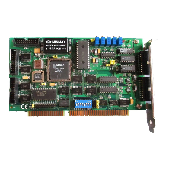
1.1 Introduction The PCL-812PG is a high performance, high speed, multi-function data acquisition card for IBM PC/XT/AT and compatible computers. The high-end specifications fo this full-sized card, and complete software support from third-party vendors makes it ideal for a wide range of applications in industrial and laboratory environments. -
Page 6: Expansion Capabilities
• 16 TTL/DTL compatible digital inputs, and 16 digital output channels. 1.3 Expansion Capabilities To complement the powerful features of the PCL-812PG, the versatility of the card can be enhanced by using the following optional daughter boards: PCLD-789 Amplifier/Multiplier Board This powerful front end analog input signal conditioning card can multiplex 16 differential inputs to one A/D input channel. -
Page 7: Software Support
1.4 Software Support The PCL-812PG also provides powerful and easy to use software driver functions which can be accessed by referring a user-defined parameter table. These driver functions simplify programming,... - Page 8 1.5.1 Analog Input (A/D Converter) Channels: 16 single-ended Resolution: 12 bits Input Range: Bipolar +/- 10V, +/- 5V, +/- 2.5 V, +/- 1.25 V, +/- 0.625 V, +/- 0.3125 V. All input ranges are software programmable. Overvoltage: Continuous +/- 30V max. Conversion type: Successive approximation Converter:...
-
Page 9: General Specifications
IRQ 2 to 7, 10, 11, 12, 14, 15 jumper selectable Enable: VIA S0, S1 and S2 of CONTROL register 1.5.7 DMA Channel Level: 1 or 3, jumper selectable Enable: Via S0, S1 and S2 of CONTROL register 1.5.8 General Specifications PCL-812PG User's Manual... - Page 10 Power consumption: +5V: typ. 500 mA, max 1A +12 V: typ. 50 mA, max 100 mA -12V: typ. 14 mA, max 20 mA I/O connector: 20 pin post header for I/O connection. Adapter available to convert to 37 pin D-type connector I/O base address: Requires 16 consecutive address locations.
-
Page 11: Initial Inspection
PCL-812PG. 2.2 Jumper Settings The PCL-812PG is designed for ease of use. There is one DIP switch and nine jumpers on the PCL-812PG card and the functions of the switch and the jumpers are discussed in this section. -
Page 12: Base Address Selection
The I/O port base address for the PCL-812PG is selectable via an 8-position DIP switch. The PCL-812PG requires 16 consecutive address locations in I/O space. Valid addresses are from hex 200 to hex 3F0;... - Page 13 OUT Signal output of the 8253 counter VREF Voltage reference Connector 1 (CN1) Analog Input (single-ended channels) A.GND A.GND A.GND A.GND A.GND A.GND A.GND A.GND A.GND A.GND Connector 2 (CN2) - Analog Output A.GND A.GND A.GND A.GND PCL-812PG User's Manual...
- Page 14 A.GND A.GND A.GND A.GND V.REF 1 A.GND V.REF 2 A.GND Connector 3 (CN3) Digital Output D.GND D.GND + 5V + 12V Connector 4 (CN4) - Digital Input D.GND D.GND + 5V + 12V Connector 5 (CN5) - Counter EX.TRG EX.TRG EX.TRG CTR1 GATE Chapter 2 General Information...
- Page 15 (save the screw to secure the interface card retaining bracket). Carefully grasp the upper edge of the PCL-812PG card. Align the hole in the retaining bracket with the hole on top of the expansion slot, and align the gold-striped edge connector with the expansion slot socket.
-
Page 16: Installation
Installation This chapter provides detailed installation information about the PCL-812PG. Sections include: • Initial inspection • Jumper settings • Connector pin assignments • Hardware installation • Software installation Chapter 2 General Information... - Page 17 PCL-812PG. 2.2 Jumper Settings The PCL-812PG is designed for ease of use. There is one DIP switch and nine jumpers on the PCL-812PG card and the functions of the switch and the jumpers are discussed in this section.
- Page 18 The I/O port base address for the PCL-812PG is selectable via an 8-position DIP switch. The PCL-812PG requires 16 consecutive address locations in I/O space. Valid addresses are from hex 200 to hex 3F0;...
- Page 19 The reference voltage of D/A converters can be the internally generated -5 or -10 V or an external reference voltage from connector CN2 pin 17 or pin 19. The reference source of D/A channel 1 (2) is selected by JP3 (4). PCL-812PG User's Manual...
-
Page 20: Connector Pin Assignment
JP9. If JP9 is set in the +/- 5V range, the analog input ranges of PCL-812PG are +/- 5V, +/- 2.5 V, +/- 1.25V, +/- 0.625V and +/- 0.3125V. If JP9 is set to the +/- 10V range, the analog input ranges are then +/- 10V, +/- 5V, +/- 2.5V,... - Page 21 OUT Signal output of the 8253 counter VREF Voltage reference Connector 1 (CN1) Analog Input (single-ended channels) A.GND A.GND A.GND A.GND A.GND A.GND A.GND A.GND A.GND A.GND Connector 2 (CN2) - Analog Output A.GND A.GND A.GND A.GND PCL-812PG User's Manual...
- Page 22 A.GND A.GND A.GND A.GND V.REF 1 A.GND V.REF 2 A.GND Connector 3 (CN3) Digital Output D.GND D.GND + 5V + 12V Connector 4 (CN4) - Digital Input D.GND D.GND + 5V + 12V Connector 5 (CN5) - Counter EX.TRG EX.TRG EX.TRG CTR1 GATE Chapter 2 General Information...
- Page 23 (save the screw to secure the interface card retaining bracket). Carefully grasp the upper edge of the PCL-812PG card. Align the hole in the retaining bracket with the hole on top of the expansion slot, and align the gold-striped edge connector with the expansion slot socket.
- Page 24 2.5 Software Disk A floppy diskette containing utility software is included with each PCL-812PG to minimize your application programming work and support the PCL-812PG calibration. The utility programs include: A comprehensive I/O driver for A/D, D/A, digital I/O and counter applications. This driver allows you to use standard...
- Page 25 19 = V.REF2 3.4 Digital Signal Connection The PCL-812PG has 16 digital input and 16 digital output channels. The digital I/O levels are TTL compatible. To transmit or receive digital signal to/from other TTL devices, the connection To receive an OPEN/SHORT signal from a switch or relay, a pull-up resistor must be added to...
- Page 26 Register Structure and Format The PCL-812PG requires 16 consecutive addresses in I/O space. The most important issue in programming the PCL-812PG is understanding the meaning of the 16 registers addressable from the selected I/O port base address. A summary map of the functions of each address and the data format of each register are given in the following sections.
- Page 27 4.7 Mode Control Register The mode control register is a write-only register using address BASE +11. This register provides the way to control the operating modes of the PCL-812PG. Data Format: A. Under internal trigger condition (JP1 is set to internal)
- Page 28 Data Format: 5.4 Trigger Mode The PCL-812PG A/D conversions can be triggered in any one of three ways - software trigger, on- board programmable pacer or external pulse trigger. The software trigger is controlled by the application program issued software command. Writing to register BASE +12 with any value causes a software trigger.
- Page 29 The DMA level selection jumper, JP5 and JP6, and the DMA enable bit in the PCL-812PG control register as well as the 8237 DMA controller registers must be set up before performing DMA operations. It is recommended that users use the PCL- 812PG driver to perform DMA operations.
Need help?
Do you have a question about the PCL-812PG and is the answer not in the manual?
Questions and answers