Table of Contents
Advertisement
Quick Links
Product Installation Guide
nterprise branch and head offices
IEM-DB-7S-RS
www.enochsystems.com
1-877-722-1116
sales@enochsystems.com
Copyright © 2013 Enoch Systems, LLC, Enoch Systems and the Enoch Systems logo are trademarks or registered trademarks of Enoch Systems, LLC and/or its affiliates in the U.S. and other countries.
Third-party trademarks mentioned are the property of their respective owners. All rights reserved.
Advertisement
Table of Contents

Related Manuals for IEI Technology IEM-DB-7S-RS


Summary of Contents for IEI Technology IEM-DB-7S-RS
- Page 1 Product Installation Guide nterprise branch and head offices IEM-DB-7S-RS www.enochsystems.com 1-877-722-1116 sales@enochsystems.com Copyright © 2013 Enoch Systems, LLC, Enoch Systems and the Enoch Systems logo are trademarks or registered trademarks of Enoch Systems, LLC and/or its affiliates in the U.S. and other countries.
-
Page 2: Quick Installation Guide
IEM-DB-7S-RS Quick Installation Guide Version 3.0 May 25, 2007 Package Contents IEM-DB-7S-RS-R30 package includes the following items: 1 x IEM-DB-7S-RS-R30 single board computer 1 x FDD cable 1 x HDD cable 1 x RS-232/422/485 cable 1 x Mini jumper pack 1 x User manual(QIG) ©2006 Copyright by IEI Technology corp. -
Page 3: Specifications
KB/MS: 2 LPT: 1 VGA: 1 USB2.0: 4 IDE Connector: 2 FDD: 1 Digital I/O: 8 bit digital I/O, 4-inpot / 4-output for Programmable IR connector: 5 pin-header Power Supply: ATX Ordering Information IEM-DB-7S-RS-R30 ATX Size 7 Slots ETX Baseboard... -
Page 4: Jumpers Setting And Connectors
Jumpers setting and Connectors CN9: IDE Connector(Bule)(IDE40) JP15: Compact Flash Mode selcet Description Description JP15 Description RESET# SLAVE MASTER JP15: Compact Flash Mode selcet JP15 Description MASTER SLAVE * For Intel.Chipset mode IOW# JP16: AT/ATX Power IOR# Mode Select JP16 Description ACK# short... -
Page 5: Clear Cmos
CN12: Floppy Connector JP5: COM2 Serial Port RI and Voitage selection Description Description Description RWC- COM2 RI PIN USE RI COM2 RI PIN USE +5V 4-5 COM2 RI PIN USE +12V INDEX# MOTEA# JP14: LCD Panel Voitage and DRVB# BL_ADJ Select DRVA# JP14 Description... - Page 6 CN11: IDE Connector(IDE44) CN37: Inverter Connector Description Description Description RESET# BL_ADJ +12V BL_EN IOW# CN34: GPIO Connector IOR# PIN Description PIN Description VCC5 ACK# GPIO0 GPIO1 INTR GPIO2 GPIO3 CABLE_ID GPIO4 GPIO5 GPIO6 GPIO7 37 HD_SELECT 0 38 HD_SELECT 1 ACTIVE# VCC5 VCC5...
- Page 7 CN36: Flat Panel TTL Conector (Hirose DF13-40DP-1.25V) Description Description VCC_FP VCC_FP VCC_FP VCC_FP 7 SMB_SDA / I_SDA FP_VS FP_CLK FP_HS FP_DE FP_ENVEE 39 SMB_SCL / I_SCL CN35: Flat panel Dual (two) Channe;LVDS Conector (Hirose DF13-30DP-1.25V) Description Description DENSEL# LVDSA_0- LVDSA_0+ LVDSA_1- LVDSA_1+ LVDSA_2-...
- Page 8 PCI Slot Connector SIGNAL PIN NO. PCI SLOT1 PCI SLOT2 PCI SLOT3 PCI SLOT4 REQ# REQ0# REQ1# REQ2# REQ3# GNT# GNT0# GNT1# GNT2# GNT3# CLOCK PCI CLK1 PCI CLK2 PCI CLK3 PCI CLK4 IDSEL AD19 AD20 AD21 AD22 INTA# INTB# INTC# INTD# X1 :USB, AUDIO, PCI...
- Page 9 X2 : ISA, GPIO Description Description Description Description VCC5 VCC5 SD15 SD14 IRQ5 MASTER# SD13 IRQ6 DREQ7 SD12 IRQ7- DACK7# SD11 SYSCLK DREQ6 SD10 REFSH# SA10 DACK6# DRQE1 SA11 DREQ5 DACK1# SA12 DACK5# MEMW# DREQ0 MEMR# DREQ3 SA13 DACK0# LA17 DACK3# SA14 IRQ14...
- Page 10 X3 : Serial Port, Print, LCD, TV OUT, Description Description Description Description LPT/FLPY# CRT_B CRT_R VCC5 CRT_G CRTHSYNC AFD# STB# DDCSCL CRTVSYNC DDCSDA LCD_PLUG# 60 ERR# IRRX 12 LSY3#/FPCLK 11 LSCLK#/B4 IRTX 14 LSY3+/LCDEN 13 LSCLK+/B5 INIT# U_RXD2 LSY2+/B3 LSY1+/B1 U_RTS2# LSY2#/B2 LSY1#/B0...
- Page 11 X4 : IDE, Compact Flash, LAN, Power Description Description Description Description IDEPIORX IDESIOWX PWGIN 5VSB IDEIOWX 53 IDESDREQR PCBEEP PS_ON 56 IDEPDREQR 55 IDESDR15 VBAT PWRBTN# IDEPDR15 IDESDR0 L1_LINK# KBINH IDEPDR0 IDESDR14 L1_ACT# IDEPDR14 IDESDR1 IDEPDR1 IDESDR13 SMB_SCL/NC 15 VCC5 VCC5 IDEPDR13 IDESDR2...
-
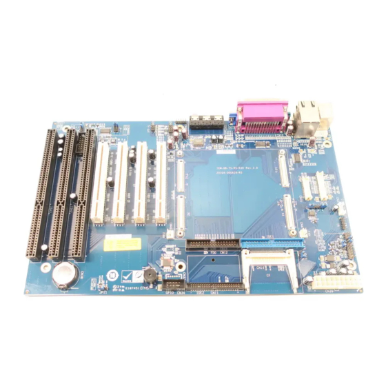
Page 12: Board Layout: Jumper And Connector Locations
Board Layout: Jumper and Connector Locations...
Need help?
Do you have a question about the IEM-DB-7S-RS and is the answer not in the manual?
Questions and answers