
Related Manuals for Aaeon AQ7-LN


Summary of Contents for Aaeon AQ7-LN
- Page 1 Q s e ve n M o d u l e A Q 7 - L N AQ7-LN ® Onboard Intel Atom N455 Processor With LCD, Ethernet PCI-Express, LPC, SMBus Audio, SATA 3.0 Gb/s AQ7-LN Manual 3rd Ed. Nov. 2013...
-
Page 2: Copyright Notice
AAEON assumes no liabilities resulting from errors or omissions in this document, or from the use of the information contained herein. AAEON reserves the right to make changes in the product design without notice to its users. - Page 3 Q s e ve n M o d u l e A Q 7 - L N Acknowledgments All other products’ name or trademarks are properties of their respective owners. AMI is a trademark of American Megatrends Inc. ® ®...
-
Page 4: Packing List
A Q 7 - L N Packing List Before you begin installing your card, please make sure that the following materials have been shipped: 1 AQ7-LN CPU Module 1 CD-ROM for manual (in PDF format) and drivers 4 M2.5 Screws If any of these items should be missing or damaged, please contact your distributor or sales representative immediately. -
Page 5: Table Of Contents
Q s e ve n M o d u l e A Q 7 - L N Contents Chapter 1 General Information 1.1 Introduction ..............1-2 1.2 Features ..............1-3 1.3 Specifications ............1-4 Chapter 2 Quick Installation Guide 2.1 Safety Precautions ............ 2-2 2.2 Location and Mechanical Drawing of Connectors and Jumpers ................ - Page 6 Q s e ve n M o d u l e A Q 7 - L N A.2 W83627DHG Watchdog Timer Initial Program ..A-7 Appendix B I/O Information B.1 I/O Address Map ............ B-2 B.2 1 MB Memory Address Map ........ B-3 B.3 IRQ Mapping Chart ..........
-
Page 7: Chapter 1 General Information
Q s e ve n M o d u l e A Q 7 - L N Chapter General Information 1 - 1 Chapter 1 General Information... -
Page 8: Introduction
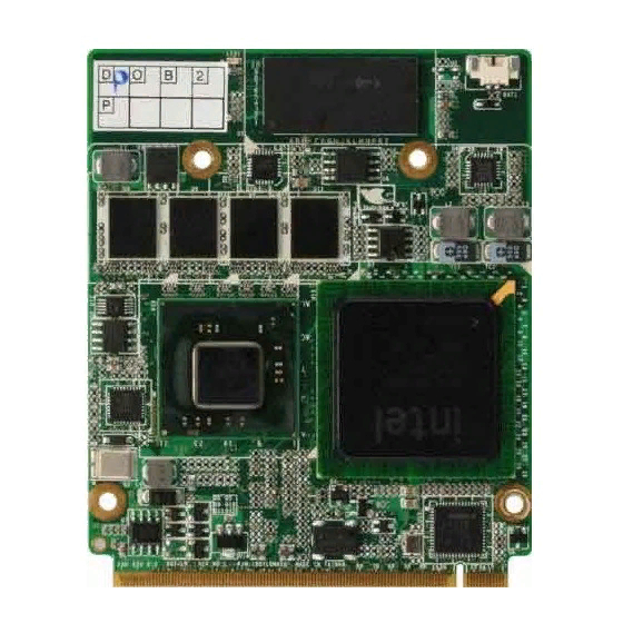
For the display specifications, AQ7-LN integrates Intel Atom™ N455 and integrates hardware MPEG2 decoder, and shared system memory is up to 384MB/DVMT 4.0. The display of AQ7-LN supports up to 18-bit single channel LVDS LCD. The AQ7-LN equips rich I/O interfaces, such as eight USB2.0 and ample storages of two SATA 2 and onboard SATA SSD for flexible storage. -
Page 9: Features
Q s e ve n M o d u l e A Q 7 - L N 1.2 Features ® Atom™ N455 Processor Onboard Intel Onboard DDR3 667 Memory, Max. 2 GB Gigabit Ethernet CRT Connector, 18-bit Single Channel LVDS LCD ... -
Page 10: Specifications
Q s e ve n M o d u l e A Q 7 - L N 1.3 Specifications System Processor ® Onboard Intel Atom™ N455 Processor Memory Onboard DDR3 667/800, Max. 2 GB ® Chipset Intel ICH8M ®... - Page 11 Q s e ve n M o d u l e A Q 7 - L N Display: Supports CRT/LVD simultaneous/ dual view displays ® Chipset Intel Atom™N455 integrated Integrates hardware MPEG2 decoder Memory Shared system memory up to 384 MB/ DVMT 4.0 ...
-
Page 12: Chapter 2 Quick Installation Guide
Q s e ve n M o d u l e A Q 7 - L N Chapter Quick Installation Guide Chapter 2 Quick Installation Guide... -
Page 13: Safety Precautions
Q s e ve n M o d u l e A Q 7 - L N 2.1 Safety Precautions Always completely disconnect the power cord from your board whenever you are working on it. Do not make connections while the power is on, because a sudden rush of power can damage sensitive electronic components. -
Page 14: Jumpers
Q s e ve n M o d u l e A Q 7 - L N 2.2 Location and Mechanical Drawing of Connectors and Jumpers Chapter 2 Quick Installation Guide... -
Page 15: List Of Jumpers
Q s e ve n M o d u l e A Q 7 - L N 2.3 List of Jumpers The board has a number of jumpers/Connectors that allow you to configure your system to suit your application. The table below shows the function of each of the board's jumpers: Function Label AT_ATX Selection/Clear CMOS Setting... -
Page 16: Vga Connector (Cn2)
Q s e ve n M o d u l e A Q 7 - L N (CN2) VGA Connector Signal CRT_RED CRT_GREEN CRT_BLUE CRT_DDC_CLK CRT_DDC_DATA CRT_HSYNC CRT_VSYNC SMI# 2.6 RTC Battery Connector (BAT1) Signal +3V_BAT 2.7 CPLD Control Switch (SW1) Signal ON ->AT mode,OFF ->ATX mode (Default) ON ->Clear CMOS,OFF ->reserve CMOS (Default) - Page 17 Q s e ve n M o d u l e A Q 7 - L N GBE_MDI3+ GBE_MDI2+ GBE_LINK100# GBE_LINK1000# GBE_MDI1- GBE_MDI0- GBE_MDI1+ GBE_MDI0+ GBE_ACT# LAN_1.8V SLP_S5# WAKE# SLP_S3# SUS_STAT# PWRBTN# SLP_BTN# LID_BTN# PWGIN BATLOW# RSTBTN# SATA_TXP0 SATA_TXP1 SATA_TXN0 SATA_TXN1 ICH_SATA_LED# SATA_RXP0...
- Page 18 Q s e ve n M o d u l e A Q 7 - L N HDA_SYNC SMBCLK HDA_RST# SMBDATA HDA_BIT_CLK SMBALERT# HDA_SDIN0 HDA_SDOUT WDTRIG# THERMTRIP# WDT_OUT USBP7N USBP6N USBP7P USBP6P OC#6_7 OC#4_5 USBP5N USBP4N USBP5P USBP4P OC#2_3 OC#0_1 USBP3N USBP2N USBP3P...
- Page 19 Q s e ve n M o d u l e A Q 7 - L N LA_CLK LA_CLK# L_BKLTCTL L_DDC_DATA LCTLB_DATA L_DDC_CLK LCTLA_CLK CLK_PCIE_100M PCIE_WAKE# CLK_PCIE_100M# PCIE_RST# ICH_PCIE_TXP3 ICH_PCIE_RXP3 ICH_PCIE_TXN3 ICH_PCIE_RXN3 ICH_PCIE_TXP2 ICH_PCIE_RXP2 ICH_PCIE_TXN2 ICH_PCIE_RXN2 Chapter 2 Quick Installation Guide...
- Page 20 Q s e ve n M o d u l e A Q 7 - L N PCIE1_RST# PCIE2_RST# ICH_PCIE_TXP1 ICH_PCIE_RXP1 ICH_PCIE_TXN1 ICH_PCIE_RXN1 PCIE1_CPPE# PCIE2_CPPE# ICH_PCIE_TXP0 ICH_PCIE_RXP0 ICH_PCIE_TXN0 ICH_PCIE_RXN0 LPC_AD0 LPC_AD1 LPC_AD2 LPC_AD3 LPC_CLK LPC_FRAME# SERIRQ LPC_LDRQ#0 RTCBAT ICH_SPKR FAN_TAC FAN_CTL SPI_SI SPI_CS#0...
- Page 21 Q s e ve n M o d u l e A Q 7 - L N +5V_EXT +5V_EXT +5V_EXT +5V_EXT 2-10 Chapter 2 Quick Installation Guide...
- Page 22 Q s e ve n M o d u l e A Q 7 - L N Below Table for China RoHS Requirements 产品中有毒有害物质或元素名称及含量 AAEON Main Board/ Daughter Board/ Backplane 有毒有害物质或元素 部件名称 铅 汞 镉 六价铬 多溴联苯 多溴二苯醚 (Pb) (Hg)
-
Page 23: Chapter 3 Ami Bios Setup
Q s e ve n M o d u l e A Q 7 - L N Chapter BIOS Setup Chapter 3 AMI BIOS Setup 3-1... -
Page 24: System Test And Initialization
3. The CMOS memory has lost power and the configuration information has been erased. The AQ7-LN CMOS memory has an integral lithium battery backup for data retention. However, you will need to replace the complete unit when it finally runs down. -
Page 25: Ami Bios Setup
Q s e ve n M o d u l e A Q 7 - L N 3.2 AMI BIOS Setup AMI BIOS ROM has a built-in Setup program that allows users to modify the basic system configuration. This type of information is stored in battery-backed CMOS RAM so that it retains the Setup information when the power is turned off. - Page 26 Q s e ve n M o d u l e A Q 7 - L N Setup Menu Main Chapter 3 AMI BIOS Setup 3-4...
- Page 27 Q s e ve n M o d u l e A Q 7 - L N Advanced Options Summary: Launch PXE OpROM Enable Optimal Default, Failsafe Default Disable Enable or Disable Boot Option for Legacy Network Devices Chapter 3 AMI BIOS Setup 3-5...
- Page 28 Q s e ve n M o d u l e A Q 7 - L N PCI Subsystem Settings Options Summary: 32 PCI Bus Clocks Optimal Default, Failsafe Default PCI Latency Timer 64 PCI Bus Clocks 96 PCI Bus Clocks 128 PCI Bus Clocks 160 PCI Bus Clocks 192 PCI Bus Clocks...
-
Page 29: Acpi Settings
Q s e ve n M o d u l e A Q 7 - L N ACPI Settings Options Summary: Enable ACPI Auto Enable Configuration Disable Optimal Default, Failsafe Default Enables or Disables BIOS ACPI Auto Configuration Enable Hibernation Enable Optimal Default, Failsafe Default Disable... - Page 30 Q s e ve n M o d u l e A Q 7 - L N Suspend mode Suspend Disabled S1 (CPU Stop Clock) S3 (Suspend to RAM) Optimal Default, Failsafe Default Select the ACPI state used for System Suspend Chapter 3 AMI BIOS Setup 3-8...
-
Page 31: Cpu Configuration
Q s e ve n M o d u l e A Q 7 - L N CPU Configuration Options Summary: Intel SpeedStep Enable Optimal Default, Failsafe Default Disable Enable or Disable Intel(R) SpeedStep(tm) Enable Optimal Default, Failsafe Hyper-Threading Default Disable En/Disable CPU Hyper-Threading function... - Page 32 Q s e ve n M o d u l e A Q 7 - L N Execute Disable Enable Optimal Default, Failsafe Default Disable Execute Disable can prevent certain classes of malicious buffer overflow attacks when combined with a supporting OS (Windows Server 2003 SP1, Windows XP SP2, SuSE Linux 9.2, RedHat Enterprise 3 Update 3.) Limit CPUID Enable...
-
Page 33: Ide Configuration
Q s e ve n M o d u l e A Q 7 - L N IDE Configuration Options Summary: ATA Or IDE Configuration Compatible Optimal Default, Failsafe Default Enhanced Select ATA or IDE configuration Configure SATA As Optimal Default, Failsafe Default RAID... - Page 34 Q s e ve n M o d u l e A Q 7 - L N Intel IGD SWSCI OpRegion Options Summary: DVMT Mode Select Fixed Mode DVMT Mode Optimal Default, Failsafe Default Select DVMT Mode used by Internal Graphics Device DVMT/FIXED 128MB Memory...
-
Page 35: Oc#4
Q s e ve n M o d u l e A Q 7 - L N Select DVMT/FIXED Mode Memory size used by Internal Graphics Device IGD – Boot Type CRT + LFP Optimal Default, Failsafe Default Select the Video Device which will be activated during POST. This has no effect if external graphics present LCD Panel Type 640x480... - Page 36 Q s e ve n M o d u l e A Q 7 - L N A Little Dark The Most Dark Select Backlight brightness of LVDS Chapter 3 AMI BIOS Setup 3-14...
-
Page 37: Usb Configuration
Q s e ve n M o d u l e A Q 7 - L N USB Configuration Options Summary: Legacy USB Support Enabled Optimal Default, Failsafe Default Disabled Auto Enables BIOS Support for Legacy USB Support. When enabled, USB can be functional in legacy environment like DOS. - Page 38 Q s e ve n M o d u l e A Q 7 - L N Floppy Forced FDD Hard Disk CDROM If Auto. USB devices less than 530MB will be emulated as Floppy and remaining as Floppy and remaining as hard drive. Forced FDD option can be used to force a HDD formatted drive to boot as FDD(Ex.
- Page 39 Q s e ve n M o d u l e A Q 7 - L N W83L786G H/W Monitor Chapter 3 AMI BIOS Setup 3-17...
-
Page 40: Super Io Configuration
Q s e ve n M o d u l e A Q 7 - L N Super IO Configuration Chapter 3 AMI BIOS Setup 3-18... - Page 41 Q s e ve n M o d u l e A Q 7 - L N Serial Port 0 Configuration Chapter 3 AMI BIOS Setup 3-19...
- Page 42 Q s e ve n M o d u l e A Q 7 - L N Serial Port 1 Configuration Options summary: Serial Port Disabled Enabled Optimal Default, Failsafe Default Allows BIOS to En/Disable correspond serial port. Change Settings Auto Optimal Default, Failsafe Default (Serial Port 1)
- Page 43 Q s e ve n M o d u l e A Q 7 - L N IO=2E8h; IRQ=10,11 Allows BIOS to Select Serial Port resource. Change Settings Auto Optimal Default, Failsafe Default (Serial Port 2) IO=2F8h; IRQ=3; IO=3F8h; IRQ=3,4; IO=2F8h;...
- Page 44 Q s e ve n M o d u l e A Q 7 - L N Digital IO Port Configuration Options summary: Input Port 1-8 Output Set GPIO as Input or Output Chapter 3 AMI BIOS Setup 3-22...
-
Page 45: Clock Generator Configuration
Q s e ve n M o d u l e A Q 7 - L N Clock Generator Configuration Options summary: PLL1 Spread Spectrum Disable Enable Optimal Default, Failsafe Default Spread Spectrum Setting for PLL1 PLL3 Spread Spectrum Disable Enable Optimal Default,... - Page 46 Q s e ve n M o d u l e A Q 7 - L N Chipset Chapter 3 AMI BIOS Setup 3-24...
- Page 47 Q s e ve n M o d u l e A Q 7 - L N Host Bridge Options summary: MMIO Size AUTO Optimal Default, Failsafe Default Set reserve memory size for MMIO Initiate Graphic Adapter Optimal Default, Failsafe Default Select which graphics controller to use as the primary boot device.
- Page 48 Q s e ve n M o d u l e A Q 7 - L N Memory Frequency and Timing Chapter 3 AMI BIOS Setup 3-26...
- Page 49 Q s e ve n M o d u l e A Q 7 - L N OnChip VGA Configuration Options summary: Share Memory Size 1 MB 8 MB Select Share Memory Size Chapter 3 AMI BIOS Setup 3-27...
-
Page 50: South Bridge
Q s e ve n M o d u l e A Q 7 - L N South Bridge Options Summary: HD Audio Controller Disabled Enable Optimal Default, Failsafe Default Enabling/Disabling HD Audio controller. USB Function Disabled Enabled Optimal Default, Failsafe Default Enabling/Disabling 8111E controller Chapter 3 AMI BIOS Setup 3-28... - Page 51 Q s e ve n M o d u l e A Q 7 - L N USB 2.0(EHCI) Support Disabled Enabled Optimal Default, Failsafe Default Enable or disable USB 2.0 (EHCI) Support SMBus Controller Disabled Enabled Optimal Default, Failsafe Default Enable or disable onchip SMBus Controller Disabled LAN1(i82567V Gbe...
- Page 52 Q s e ve n M o d u l e A Q 7 - L N SLP_S4 Assertion Width 1-2 Seconds 2-3 Seconds 3-4 Seconds Optimal Default, Failsafe Default 4-5 Seconds Select a minimum assertion width of the SLP_S4# signal Restore on AC Power Power Off Optimal Default,...
- Page 53 Q s e ve n M o d u l e A Q 7 - L N Boot Options Summary: Bootup NumLock Optimal Default, Failsafe Default State Select the keyboard NumLock state Quiet Boot Disabled Enabled Optimal Default, Failsafe Default En/Disable showing boot logo.
- Page 54 Q s e ve n M o d u l e A Q 7 - L N UPON REQUEST - GA20 can be disabled using BIOS services. ALWAYS - do not allow disabling GA20; this option is useful when any RT code is executed above 1MB.
- Page 55 Q s e ve n M o d u l e A Q 7 - L N Security Change User/Supervisor Password You can install a Supervisor password, and if you install a supervisor password, you can then install a user password. A user password does not provide access to many of the features in the Setup utility.
- Page 56 Q s e ve n M o d u l e A Q 7 - L N Setup utility. Removing the Password Highlight this item and type in the current password. At the next dialog box press Enter to disable password protection. ...
-
Page 57: Chapter 4 Driver Installation
Q s e ve n M o d u l e A Q 7 - L N Chapter Driver Installation Chapter 4 Driver Installation... - Page 58 Q s e ve n M o d u l e A Q 7 - L N The AQ7-LN comes with a CD-ROM that contains all drivers and utilities that meet your needs. Follow the sequence below to install the drivers: Step 1 –...
- Page 59 Q s e ve n M o d u l e A Q 7 - L N 4.1 Installation: Insert the AQ7-LN CD-ROM into the CD-ROM Drive. And install the drivers from Step 1 to Step 5 in order. Step 1 – Install Chipset Driver 1.
- Page 60 Q s e ve n M o d u l e A Q 7 - L N Step 4 – Install LAN Driver 1. Click on the STEP4-LAN folder and select the folder of OS your system is 2. Double click on the .exe file located in each OS folder 3.
-
Page 61: Appendix A Programming The Watchdog Timer
Q s e ve n M o d u l e A Q 7 - L N Appendix Programming the Watchdog Timer Appendix A Programming the Watchdog Timer... -
Page 62: Programming
AQ7-LN utilizes W83627DHG-P chipset as its watchdog timer controller. Below are the procedures to complete its configuration and the AAEON intial watchdog timer program is also attached based on which you can develop customized program to fit your application. Configuring Sequence Description... - Page 63 Q s e ve n M o d u l e A Q 7 - L N (3) Exit the W83627DHG config Mode. Undesired result may occur if the config Mode is not exited normally. (1) Enter the W83627DHG config Mode To enter the W83627DHG config Mode, two special I/O write operations are to be performed during Wait for Key state.
- Page 64 Q s e ve n M o d u l e A Q 7 - L N = 010 Power LED pin is driven low. = 011 Power LED pin outputs 2Hz pulse with 50% duty cycle. = 100 Power LED pin outputs 1Hz pulse with 50% duty cycle.
- Page 65 Q s e ve n M o d u l e A Q 7 - L N WatchDog Timer Register II (Index=F6h, Default=00h) Bit 7-0 = 0 x 00 Time-out Disable = 0 x 01 Time-out occurs after 1 second/minute = 0 x 02 Time-out occurs after 2 second/minutes = 0 x 03 Time-out occurs after 3...
- Page 66 Q s e ve n M o d u l e A Q 7 - L N Force Watchdog Timer time-out event: this bit is self-clearing Bit 4 : Watchdog Timer Status. R/W Watchdog Timer time-out occurred Watchdog Timer counting Bit 3-0 : These bits select IRQ resource for Watchdog.
-
Page 67: W83627Dhg Watchdog Timer Initial Program
Q s e ve n M o d u l e A Q 7 - L N A.2 W83627DHG Watchdog Timer Initial Program Example: Setting 10 sec. as Watchdog timeout interval ;/////////////////////////////////////////////////////////////////////////////////////////////// Mov dx,2eh ;Enter W83627DHG config mode Mov al,87h (out 87h to 2eh twice) Out dx,al Out dx,al... - Page 68 Q s e ve n M o d u l e A Q 7 - L N ;/////////////////////////////////////////////////////////////////////////////////////////////// Dec dx Mov al,0f5h ;CRF5 (PLED mode register) Out dx,al Inc dx In al,dx And al,not 08h ;Set second as counting unit Out dx,al ;/////////////////////////////////////////////////////////////////////////////////////////////// Dec dx...
-
Page 69: Appendix B I/O Information
Q s e ve n M o d u l e A Q 7 - L N Appendix I/O Information B - 1 Appendix B I/O Information... -
Page 70: I/O Address Map
Q s e ve n M o d u l e A Q 7 - L N B.1 I/O Address Map B - 2 Appendix B I/O Information... -
Page 71: St Mb Memory Address Map
Q s e ve n M o d u l e A Q 7 - L N B.2 1 MB Memory Address Map B - 3 Appendix B I/O Information... -
Page 72: Irq Mapping Chart
Q s e ve n M o d u l e A Q 7 - L N B.3 IRQ Mapping Chart B.4 DMA Channel Assignments B - 4 Appendix B I/O Information...
Need help?
Do you have a question about the AQ7-LN and is the answer not in the manual?
Questions and answers