
Related Manuals for Xilinx VCU1525


Summary of Contents for Xilinx VCU1525
- Page 1 VCU1525 Reconfigurable Acceleration Platform User Guide UG1268 (v1.0) November 13, 2017...
-
Page 2: Revision History
Revision History The following table shows the revision history for this document. Date Version Revision 11/13/2017 Initial Xilinx release. VCU1525 Acceleration Platform User Guide Send Feedback UG1268 (v1.0) November 13, 2017 www.xilinx.com... -
Page 3: Table Of Contents
Installing the VCU1525 Board in a Server Chassis ....... . . - Page 4 Xilinx Resources ........
-
Page 5: Chapter 1: Introduction
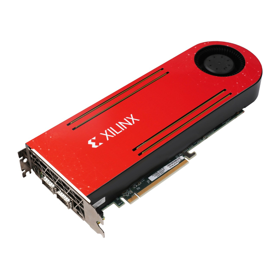
XCVU9P-L2FSGD2104E FPGA. This Xilinx FPGA-based PCIe accelerator board is designed to accelerate compute-intensive applications like machine learning, data analytics, and video processing. The VCU1525 board is available in both active and passive cooling configurations and designed to be used in cloud data center servers. Figure 1-1 shows the VCU1525 active cooling configuration (PC applications). - Page 6 X20018-110217 Figure 1-2: VCU1525 Reconfigurable Acceleration Platform (Passive Cooling) The VCU1525 board with passive cooling is designed to be installed into a data center CAUTION! server, where controlled air flow provides direct cooling. The VCU1525 board with active cooling is designed to be installed into a PC environment where the air flow is uncontrolled, hence this configuration has the heat sink and fan enclosure cover installed to provide appropriate cooling.
-
Page 7: Block Diagram
PCIe GEN1/2/3 x 1/2/4/8/16 PCIe GEN4 x 8 X19964-110617 Figure 1-3: VCU1525 Board Block Diagram Board Features The VCU1525 board features are listed in this section. Detailed information for each feature is provided in Component Descriptions Chapter • Virtex UltraScale+ XCVU9P-L2FSGD2104E FPGA •... - Page 8 Front panel JTAG and universal asynchronous receiver-transmitter (UART) access through the USB port • FPGA configurable over USB/JTAG and Quad SPI configuration flash memory • Thermal management with variable rate fan for minimal fan noise VCU1525 Acceleration Platform User Guide Send Feedback UG1268 (v1.0) November 13, 2017 www.xilinx.com...
-
Page 9: Board Specifications
Operating: 0°C to +45°C Storage: –25°C to +60°C Humidity 10% to 90% non-condensing Operating Voltage PCIe slot +12 V , +3.3 V , +3.3 V , External +12 V AUXDC VCU1525 Acceleration Platform User Guide Send Feedback UG1268 (v1.0) November 13, 2017 www.xilinx.com... -
Page 10: Chapter 2: Board Setup And Configuration
Chapter 2 Board Setup and Configuration Board Component Location Figure 2-1 shows the location of components on the VCU1525 board. Each component shown is keyed to Table 2-1. Table 2-1 identifies the components, references the respective schematic page numbers, and links to a detailed functional description of the component... - Page 11 Chapter 2: Board Setup and Configuration The VCU1525 board can be damaged by electrostatic discharge (ESD). Follow standard ESD CAUTION! prevention measures when handling the board. Table 2-1: VCU1525 Board Component Descriptions Feature Schematic Number Ref Des Notes (Link) Page...
-
Page 12: Default Switch Settings
PROGRAM_B Installing the VCU1525 Board in a Server Chassis Follow the server manufacturer's instructions for add-in board installation. FPGA Configuration The VCU1525 board supports two UltraScale+ FPGA configuration modes: • Quad SPI flash memory • JTAG using USB JTAG configuration port (USB J13/FT4232H U27) The FPGA bank 0 mode pins are hardwired to M[2:0] = 001 Master SPI mode with pull-up/down resistors. - Page 13 [Ref Table 2-4: Configuration Modes Configuration Mode M[2:0] Bus Width CCLKL Direction Master SPI x1, x2, x4 FPGA output JTAG Not applicable - JTAG overrides Not applicable VCU1525 Acceleration Platform User Guide Send Feedback UG1268 (v1.0) November 13, 2017 www.xilinx.com...
- Page 14 Chapter 2: Board Setup and Configuration The configuration circuit is shown in Figure 2-2. X-Ref Target - Figure 2-2 X19973-103017 Figure 2-2: VCU1525 Configuration Circuit VCU1525 Acceleration Platform User Guide Send Feedback UG1268 (v1.0) November 13, 2017 www.xilinx.com...
-
Page 15: Chapter 3: Board Component Descriptions
For more information on Virtex UltraScale+ FPGAs, see Virtex UltraScale+ FPGA Data Sheet: DC and AC Switching Characteristics (DS923) [Ref I/O Voltage Rails There are 13 I/O banks available on the XCVU9P-L2FSGD2104E FPGA and the VCU1525 board. VCU1525 Acceleration Platform User Guide Send Feedback UG1268 (v1.0) November 13, 2017... - Page 16 Bank 66 VCC1V2_BTM 1.2V DDR4 C1 DQ[32:63] Bank 67 VCC1V8_BTM 1.2V DDR4 C1 DQ[0:31] Bank 69 VCC1V2_TOP 1.2V DDR4_C2 DQ[32:71] Bank 70 VCC1V2_TOP 1.2V DDR4 C2 DQ[40:47], ADDR/CTRL VCU1525 Acceleration Platform User Guide Send Feedback UG1268 (v1.0) November 13, 2017 www.xilinx.com...
-
Page 17: Ddr4 Dimm Memory
Two Quad Serial Peripheral Interface (SPI) flash memory devices of the same type and wired in parallel are provided on the VCU1525 board (U17 and U58). A field effect transistor (FET) switch structure (U57 and U61) implements a chip-select enable mechanism, controlled by the MSP432 board management controller (BMC). - Page 18 Datapath width: 4 bits • Data rate: variable Figure 3-2 shows the linear Quad SPI flash memory circuitry on the VCU1525 board. For more flash memory details, see the Micron MT25QU01GBB8E12-0SIT data sheet at the Micron website [Ref X-Ref Target - Figure 3-2...
-
Page 19: Usb Jtag Interface
[Figure 2-1, callout 7] The VCU1525 board XCVU9P-L2FSGD2104E FPGA U13 is the only component in the Joint Test Action Group (JTAG) chain. JTAG configuration is available through the USB-to-JTAG FTDI FT4232HQ U27 bridge device connected to Micro-AB USB connector J13. The FTDI JTAG signals are level-shifted through TXBN0304 device U35. -
Page 20: Ft4232Hq Usb-Uart Interface
Chapter 3: Board Component Descriptions FT4232HQ USB-UART Interface [Figure 2-1, callout 7] The FT4232HQ U27 Quad USB-UART on the VCU1525 board provides two UART connections through the single Micro-AB USB connector J13. • Channel AD is configured to support the JTAG chain. - Page 21 FT2232H_UART_TX ACBUS0 The VCU1525 revision D board implements a second USB connector. J17 is a keyed 1.2 mm right-angle receptacle (Amphenol 10125839-04RAEHLF). J17 is selectable via TI TS3USB221RSER 1-to-2 USB switch U59, which is controlled by the MSP432 U19 BMC. USB switch U59 selects between the Micro-AB USB connector J13 (port 1) and the J17 4-pin receptacle (port 2).
-
Page 22: Clock Generation
The TS3USB221RSER data sheet is available on the TI website [Ref Clock Generation [Figure 2-1, callout 10, 11, 12] The VCU1525 board provides eight clock sources to the XCVU9P-L2FSGD2104E device, listed in Table 3-4. Table 3-4: VCU1525 Board Clock Sources Clock Name Clock Ref. - Page 23 Chapter 3: Board Component Descriptions Table 3-4: VCU1525 Board Clock Sources (Cont’d) Clock Name Clock Ref. Des. Description USER_SI570_CLOCK U43 (Q0) Silicon Labs Si53340 3.3V LVDS clock buffer. USER_SI570_CLOCK_P/N GPIO I/F bank 64. MGT SI570 CLOCK0 (QSFP0) U43 (Q2) Silicon Labs Si53340 3.3V LVDS clock buffer.
- Page 24 Chapter 3: Board Component Descriptions The VCU1525 clocking diagram is shown in Figure 3-3. X-Ref Target - Figure 3-6 U13AF BANK 63 DDR4 C0 I/F SYSCLK0_300_/P/N AY37/AY38 GC QBC XCVU9PFSGD2104 SYSCLK1_300_P/N U13Z BANK 70 SYSCLK2_300_P/N DDR4 C2 I/F F32/E32 GC QBC...
-
Page 25: System Clock And Qsfp0 Clock
QSFP0 interface GTY bank 231 MGTREFCLK1 P/N input pins K11 and K10. • CLK2A is not used • CLK3A is not used. The FPGA connections for each clock are listed in Appendix A, Master Constraints File Listing. VCU1525 Acceleration Platform User Guide Send Feedback UG1268 (v1.0) November 13, 2017 www.xilinx.com... - Page 26 Figure 3-7: 300MHz and QSFP0 156.25MHz Clock Source The 300 MHz clock buffer Si53340 U44 is shown in Figure 3-7. X-Ref Target - Figure 3-8 X19976-103017 Figure 3-8: 300 MHz Clock Buffer VCU1525 Acceleration Platform User Guide Send Feedback UG1268 (v1.0) November 13, 2017 www.xilinx.com...
-
Page 27: Qsfp1 Clock
QSFP1 interface GTY bank 230 MGTREFCLK1P/N input pins P11 and P10. • CLK2A: is not used. • CLK3A is not used. • The FPGA connections for each clock are listed in Appendix A, Master Constraints File Listing. VCU1525 Acceleration Platform User Guide Send Feedback UG1268 (v1.0) November 13, 2017 www.xilinx.com... -
Page 28: Programmable Mgt And User Clock
On power-up, the SI570 user clock defaults to an output frequency of 156.250MHz. User applications can change the output frequency within the range of 10MHz to 810 MHz through an inter IC (I2C) interface. Power cycling the VCU1525 board resets this clock to the default frequency of 156.250MHz. -
Page 29: Gty Transceivers
Figure 3-10: USER and MGT SI570 Clock Circuit GTY Transceivers [Figure 2-1, callout 1] The VCU1525 board provides access to 24 of the 76 GTY transceivers: • Four GTY transceivers (bank 231) are wired to QSFP28 connector QSFP0 J7. •... - Page 30 The GTY transceivers in the XCVU9P-L2FSGD2104E are grouped into four channels or quads. The reference clock for a quad can be sourced from the quad above or the quad below the GTY quad of interest. The six GTY quads used on the VCU1525 board have the following connectivity (also see...
-
Page 31: Pci Express Endpoint Connectivity
85 Ω ±10%. The PCIe clock is routed as a 100 Ω differential pair. The FPGA GTY MGT connections for the 16-lane PCIe connector are listed in Appendix A, Master Constraints File Listing. VCU1525 Acceleration Platform User Guide Send Feedback UG1268 (v1.0) November 13, 2017 www.xilinx.com... -
Page 32: Gb/S Qsfp+ Module Connectors
[Figure 2-1, callout 13, 14] The VCU1525 board hosts dual quad (4-channel) small form-factor pluggable (28 Gb/s QSFP+) connectors (QSFP0 J7, QSFP1 J9) that accept 28 Gb/s and below QSFP+ optical modules. Each connector is housed within a single 28 Gb/s QSFP+ cage assembly. QSFP0 J7 RX/TX lanes are wired to GTY bank/quad 231, and QSFP1 J9 RX/TX lanes are wired to GTY bank/quad 230. -
Page 33: I2C Bus
Technology Affiliates website [Ref I2C Bus The VCU1525 board implements two I2C bus networks, I2C_FPGA_SDA/SCL (4-chan. PCA9546 U28 at address 0b1110100/0x74) connected to the XCVU9P-L2FSGD2104E U13 only, and I2C_MAIN_SDA/SCL (4-chan. PCA9546 U56 at address 0b1110101/0x75) which is connected to the MSP432 U19 BMC only. - Page 34 U28 bus switch at I2C address 0x74 (0b1110100). VCU1525 U28 PCA9546 bus switch hosts both a Si570 programmable clock and an 8-Kbit M24C08 EEPROM on the USER_SI570_CLOCK_SDA/SCL channel 2 I2C bus.
- Page 35 U56 bus switch at I2C address 0x75 (0b1110101). VCU1525 U56 PCA9546 bus switch hosts three NXP SE98ATP thermal sensors plus a TI PCA9536 4-bit port expander and an 8-Kbit M24C08 EEPROM on the IIC_SDA/SCL_EEPROM channel 1 I2C bus.
- Page 36 Chapter 3: Board Component Descriptions The VCU1525 board I2C_FPGA_SDA/SCL bus topology is shown in Figure 3-14. X-Ref Target - Figure 3-14 X19967-110217 Figure 3-14: I2C_FPGA_SDA/SCL Bus Topology Table 3-6 lists the I2C address of the PCA9546 U56 bus switch target devices.
-
Page 37: Status Leds
1. This connection allows the MSP432 U19 to access the U28 switch target devices and FPGA U13. Status LEDs The VCU1525 board is designed to operate with the heat sink and fan enclosure cover installed. Status light emitting diode (LED) DS3 is a triple-stack LED which is visible through a cut-out in the PCIe end bracket. - Page 38 3, 5 would represent two instantiations of Timer_A, the first instantiation having 3 and the second instantiation having 5 capture/compare registers and PWM output generators, respectively. VCU1525 Acceleration Platform User Guide Send Feedback UG1268 (v1.0) November 13, 2017...
- Page 39 EEPROM/TMP QSFP0 SNSR QSFP QSFP1 I2C connection to FPGA FAN CONT Unused Mux Port SI570 EEPROM EEPROM for IP keys X20040-110917 Figure 3-15: U19 MSP432 I2C Connectivity VCU1525 Acceleration Platform User Guide Send Feedback UG1268 (v1.0) November 13, 2017 www.xilinx.com...
- Page 40 U19 MSP432 circuit. See the schematic 0381795 (Rev. D) sheet 24 for finer details [Ref X-Ref Target - Figure 3-16 X20012-110117 Figure 3-16: MSP432 Circuit VCU1525 Acceleration Platform User Guide Send Feedback UG1268 (v1.0) November 13, 2017 www.xilinx.com...
- Page 41 U19 MSP432. See schematic 0381795 (Rev. D) sheet 24 for finer details. [Ref X-Ref Target - Figure 3-17 X20013-110117 Figure 3-17: MSP432 Voltage and Sense Points VCU1525 Acceleration Platform User Guide Send Feedback UG1268 (v1.0) November 13, 2017 www.xilinx.com...
-
Page 42: Vcu1525 Board Power System
Chapter 3: Board Component Descriptions VCU1525 Board Power System The VCU1525 board hosts a Linear Technology based power system. Essential input power rails are sourced from the 16-lane PCIe connector CN1 through pins A2, A3, B1, and B2 12V_IN (12V), A9, A10, and B8 3V3_PEX_IN (3.3V) and B10 3V3AUX (3.3V). -
Page 43: Monitoring Voltage And Current
Chapter 3: Board Component Descriptions The VCU1525 board uses power regulators from Linear Technology to supply the core and auxiliary voltages. The V 2-phase (of 6) regulator U41 is PMBus-compliant. The power CCINT system regulators are listed in Table 3-9. -
Page 44: Board Management Controller Voltage Measurements
CCBRAM displayed via the SYSMON internal voltage measurement capability. Board Management Controller Voltage Measurements The VCU1525 MSP432 U19 board management controller ADC interface allows additional power system voltage measuring capability. The VCU1525 voltage rail-to-ADC channel assignments are listed in Table 3-10. -
Page 45: Vccint Regulator Circuit
CCINT DCR measurement techniques. Vccint Regulator Circuit The VCU1525 PCIe CN1 edge connector provides limited 12V power (5.5 amperes max.). The power circuit is comprised of six phases to allow a two-step additional power CCINT increase when the auxiliary 12V power is applied through the 2x4 power connector JP1,... - Page 46 0 of the U56 PCA9546 I2C mux (address 0x75) as shown in the I2C Bus section of this document.The LM96063 over-temperature TCRIT# output is wired to a MAX16052 (U3) supervisory device which turns off the VCU1525 power system voltage regulators if an over-temperature event is detected. See the LM96063...
-
Page 47: Appendix A: Master Constraints File Listing
Master Constraints File Listing Overview The master Xilinx® design constraints (XDC) file template for the VCU1525 board provides for designs targeting the VCU1525 reconfigurable acceleration platform. Net names in the constraints listed correlate with net names on the latest VCU1525 board schematic. You must identify the appropriate pins and replace the net names with net names in the user RTL. - Page 48 [get_ports DDR4_C0_ADR15]; set_property IOSTANDARD SSTL12_DCI [get_ports DDR4_C0_ADR15]; set_property PACKAGE_PIN AR36 [get_ports DDR4_C0_ADR16]; set_property IOSTANDARD SSTL12_DCI [get_ports DDR4_C0_ADR16]; set_property PACKAGE_PIN AN35 [get_ports DDR4_C0_ADR17]; set_property IOSTANDARD SSTL12_DCI [get_ports DDR4_C0_ADR17]; VCU1525 Acceleration Platform User Guide Send Feedback UG1268 (v1.0) November 13, 2017 www.xilinx.com...
- Page 49 [get_ports DDR4_C0_DQ5]; set_property PACKAGE_PIN BC27 [get_ports DDR4_C0_DQ6]; set_property IOSTANDARD POD12_DCI [get_ports DDR4_C0_DQ6]; set_property PACKAGE_PIN BB27 [get_ports DDR4_C0_DQ7]; set_property IOSTANDARD POD12_DCI [get_ports DDR4_C0_DQ7]; set_property PACKAGE_PIN BE28 [get_ports DDR4_C0_DQ8]; VCU1525 Acceleration Platform User Guide Send Feedback UG1268 (v1.0) November 13, 2017 www.xilinx.com...
- Page 50 [get_ports DDR4_C0_DQ35]; set_property IOSTANDARD POD12_DCI [get_ports DDR4_C0_DQ35]; set_property PACKAGE_PIN AN31 [get_ports DDR4_C0_DQ36]; set_property IOSTANDARD POD12_DCI [get_ports DDR4_C0_DQ36]; set_property PACKAGE_PIN AN32 [get_ports DDR4_C0_DQ37]; set_property IOSTANDARD POD12_DCI [get_ports DDR4_C0_DQ37]; VCU1525 Acceleration Platform User Guide Send Feedback UG1268 (v1.0) November 13, 2017 www.xilinx.com...
- Page 51 [get_ports DDR4_C0_DQ64]; set_property PACKAGE_PIN BD39 [get_ports DDR4_C0_DQ65]; set_property IOSTANDARD POD12_DCI [get_ports DDR4_C0_DQ65]; set_property PACKAGE_PIN BF43 [get_ports DDR4_C0_DQ66]; set_property IOSTANDARD POD12_DCI [get_ports DDR4_C0_DQ66]; set_property PACKAGE_PIN BF42 [get_ports DDR4_C0_DQ67]; VCU1525 Acceleration Platform User Guide Send Feedback UG1268 (v1.0) November 13, 2017 www.xilinx.com...
- Page 52 [get_ports DDR4_C0_DQS_C11]; set_property IOSTANDARD DIFF_POD12 [get_ports DDR4_C0_DQS_C11]; set_property PACKAGE_PIN BC31 [get_ports DDR4_C0_DQS_T11]; set_property IOSTANDARD DIFF_POD12 [get_ports DDR4_C0_DQS_T11]; set_property PACKAGE_PIN BA33 [get_ports DDR4_C0_DQS_C12]; set_property IOSTANDARD DIFF_POD12 [get_ports DDR4_C0_DQS_C12]; VCU1525 Acceleration Platform User Guide Send Feedback UG1268 (v1.0) November 13, 2017 www.xilinx.com...
- Page 53 [get_ports DDR4_C1_ADR14]; set_property PACKAGE_PIN AM25 [get_ports DDR4_C1_ADR15]; set_property IOSTANDARD SSTL12_DCI [get_ports DDR4_C1_ADR15]; set_property PACKAGE_PIN AN23 [get_ports DDR4_C1_ADR16]; set_property IOSTANDARD SSTL12_DCI [get_ports DDR4_C1_ADR16]; set_property PACKAGE_PIN AM24 [get_ports DDR4_C1_ADR17]; VCU1525 Acceleration Platform User Guide Send Feedback UG1268 (v1.0) November 13, 2017 www.xilinx.com...
- Page 54 PACKAGE_PIN BE10 [get_ports DDR4_C1_DQ5]; set_property IOSTANDARD POD12_DCI [get_ports DDR4_C1_DQ5]; set_property PACKAGE_PIN [get_ports DDR4_C1_DQ6]; set_property IOSTANDARD POD12_DCI [get_ports DDR4_C1_DQ6]; set_property PACKAGE_PIN [get_ports DDR4_C1_DQ7]; set_property IOSTANDARD POD12_DCI [get_ports DDR4_C1_DQ7]; VCU1525 Acceleration Platform User Guide Send Feedback UG1268 (v1.0) November 13, 2017 www.xilinx.com...
- Page 55 [get_ports DDR4_C1_DQ34]; set_property PACKAGE_PIN BD13 [get_ports DDR4_C1_DQ35]; set_property IOSTANDARD POD12_DCI [get_ports DDR4_C1_DQ35]; set_property PACKAGE_PIN BD15 [get_ports DDR4_C1_DQ36]; set_property IOSTANDARD POD12_DCI [get_ports DDR4_C1_DQ36]; set_property PACKAGE_PIN BD16 [get_ports DDR4_C1_DQ37]; VCU1525 Acceleration Platform User Guide Send Feedback UG1268 (v1.0) November 13, 2017 www.xilinx.com...
- Page 56 [get_ports DDR4_C1_DQ64]; set_property IOSTANDARD POD12_DCI [get_ports DDR4_C1_DQ64]; set_property PACKAGE_PIN BF24 [get_ports DDR4_C1_DQ65]; set_property IOSTANDARD POD12_DCI [get_ports DDR4_C1_DQ65]; set_property PACKAGE_PIN BD25 [get_ports DDR4_C1_DQ66]; set_property IOSTANDARD POD12_DCI [get_ports DDR4_C1_DQ66]; VCU1525 Acceleration Platform User Guide Send Feedback UG1268 (v1.0) November 13, 2017 www.xilinx.com...
- Page 57 DIFF_POD12 [get_ports DDR4_C1_DQS_T10]; set_property PACKAGE_PIN [get_ports DDR4_C1_DQS_C11]; set_property IOSTANDARD DIFF_POD12 [get_ports DDR4_C1_DQS_C11]; set_property PACKAGE_PIN BA10 [get_ports DDR4_C1_DQS_T11]; set_property IOSTANDARD DIFF_POD12 [get_ports DDR4_C1_DQS_T11]; set_property PACKAGE_PIN AP14 [get_ports DDR4_C1_DQS_C12]; VCU1525 Acceleration Platform User Guide Send Feedback UG1268 (v1.0) November 13, 2017 www.xilinx.com...
- Page 58 PACKAGE_PIN [get_ports DDR4_C2_ADR14]; set_property IOSTANDARD SSTL12_DCI [get_ports DDR4_C2_ADR14]; set_property PACKAGE_PIN [get_ports DDR4_C2_ADR15]; set_property IOSTANDARD SSTL12_DCI [get_ports DDR4_C2_ADR15]; set_property PACKAGE_PIN [get_ports DDR4_C2_ADR16]; set_property IOSTANDARD SSTL12_DCI [get_ports DDR4_C2_ADR16]; VCU1525 Acceleration Platform User Guide Send Feedback UG1268 (v1.0) November 13, 2017 www.xilinx.com...
- Page 59 IOSTANDARD POD12_DCI [get_ports DDR4_C2_DQ4]; set_property PACKAGE_PIN [get_ports DDR4_C2_DQ5]; set_property IOSTANDARD POD12_DCI [get_ports DDR4_C2_DQ5]; set_property PACKAGE_PIN [get_ports DDR4_C2_DQ6]; set_property IOSTANDARD POD12_DCI [get_ports DDR4_C2_DQ6]; set_property PACKAGE_PIN [get_ports DDR4_C2_DQ7]; VCU1525 Acceleration Platform User Guide Send Feedback UG1268 (v1.0) November 13, 2017 www.xilinx.com...
- Page 60 PACKAGE_PIN [get_ports DDR4_C2_DQ34]; set_property IOSTANDARD POD12_DCI [get_ports DDR4_C2_DQ34]; set_property PACKAGE_PIN [get_ports DDR4_C2_DQ35]; set_property IOSTANDARD POD12_DCI [get_ports DDR4_C2_DQ35]; set_property PACKAGE_PIN [get_ports DDR4_C2_DQ36]; set_property IOSTANDARD POD12_DCI [get_ports DDR4_C2_DQ36]; VCU1525 Acceleration Platform User Guide Send Feedback UG1268 (v1.0) November 13, 2017 www.xilinx.com...
- Page 61 IOSTANDARD POD12_DCI [get_ports DDR4_C2_DQ63]; set_property PACKAGE_PIN [get_ports DDR4_C2_DQ64]; set_property IOSTANDARD POD12_DCI [get_ports DDR4_C2_DQ64]; set_property PACKAGE_PIN [get_ports DDR4_C2_DQ65]; set_property IOSTANDARD POD12_DCI [get_ports DDR4_C2_DQ65]; set_property PACKAGE_PIN [get_ports DDR4_C2_DQ66]; VCU1525 Acceleration Platform User Guide Send Feedback UG1268 (v1.0) November 13, 2017 www.xilinx.com...
- Page 62 PACKAGE_PIN [get_ports DDR4_C2_DQS_T10]; set_property IOSTANDARD DIFF_POD12 [get_ports DDR4_C2_DQS_T10]; set_property PACKAGE_PIN [get_ports DDR4_C2_DQS_C11]; set_property IOSTANDARD DIFF_POD12 [get_ports DDR4_C2_DQS_C11]; set_property PACKAGE_PIN [get_ports DDR4_C2_DQS_T11]; set_property IOSTANDARD DIFF_POD12 [get_ports DDR4_C2_DQS_T11]; VCU1525 Acceleration Platform User Guide Send Feedback UG1268 (v1.0) November 13, 2017 www.xilinx.com...
- Page 63 IOSTANDARD SSTL12_DCI [get_ports DDR4_C3_ADR13]; set_property PACKAGE_PIN [get_ports DDR4_C3_ADR14]; set_property IOSTANDARD SSTL12_DCI [get_ports DDR4_C3_ADR14]; set_property PACKAGE_PIN [get_ports DDR4_C3_ADR15]; set_property IOSTANDARD SSTL12_DCI [get_ports DDR4_C3_ADR15]; set_property PACKAGE_PIN [get_ports DDR4_C3_ADR16]; VCU1525 Acceleration Platform User Guide Send Feedback UG1268 (v1.0) November 13, 2017 www.xilinx.com...
- Page 64 PACKAGE_PIN [get_ports DDR4_C3_DQ4]; set_property IOSTANDARD POD12_DCI [get_ports DDR4_C3_DQ4]; set_property PACKAGE_PIN [get_ports DDR4_C3_DQ5]; set_property IOSTANDARD POD12_DCI [get_ports DDR4_C3_DQ5]; set_property PACKAGE_PIN [get_ports DDR4_C3_DQ6]; set_property IOSTANDARD POD12_DCI [get_ports DDR4_C3_DQ6]; VCU1525 Acceleration Platform User Guide Send Feedback UG1268 (v1.0) November 13, 2017 www.xilinx.com...
- Page 65 IOSTANDARD POD12_DCI [get_ports DDR4_C3_DQ33]; set_property PACKAGE_PIN [get_ports DDR4_C3_DQ34]; set_property IOSTANDARD POD12_DCI [get_ports DDR4_C3_DQ34]; set_property PACKAGE_PIN [get_ports DDR4_C3_DQ35]; set_property IOSTANDARD POD12_DCI [get_ports DDR4_C3_DQ35]; set_property PACKAGE_PIN [get_ports DDR4_C3_DQ36]; VCU1525 Acceleration Platform User Guide Send Feedback UG1268 (v1.0) November 13, 2017 www.xilinx.com...
- Page 66 PACKAGE_PIN [get_ports DDR4_C3_DQ63]; set_property IOSTANDARD POD12_DCI [get_ports DDR4_C3_DQ63]; set_property PACKAGE_PIN [get_ports DDR4_C3_DQ64]; set_property IOSTANDARD POD12_DCI [get_ports DDR4_C3_DQ64]; set_property PACKAGE_PIN [get_ports DDR4_C3_DQ65]; set_property IOSTANDARD POD12_DCI [get_ports DDR4_C3_DQ65]; VCU1525 Acceleration Platform User Guide Send Feedback UG1268 (v1.0) November 13, 2017 www.xilinx.com...
- Page 67 IOSTANDARD DIFF_POD12 [get_ports DDR4_C3_DQS_C10]; set_property PACKAGE_PIN [get_ports DDR4_C3_DQS_T10]; set_property IOSTANDARD DIFF_POD12 [get_ports DDR4_C3_DQS_T10]; set_property PACKAGE_PIN [get_ports DDR4_C3_DQS_C11]; set_property IOSTANDARD DIFF_POD12 [get_ports DDR4_C3_DQS_C11]; set_property PACKAGE_PIN [get_ports DDR4_C3_DQS_T11]; VCU1525 Acceleration Platform User Guide Send Feedback UG1268 (v1.0) November 13, 2017 www.xilinx.com...
- Page 68 IOSTANDARD LVCMOS12 [get_ports QSFP0_REFCLK_RESET]; set_property PACKAGE_PIN BE17 [get_ports QSFP0_RESETL_LS]; set_property IOSTANDARD LVCMOS12 [get_ports QSFP0_RESETL_LS]; # QSFP1 set_property PACKAGE_PIN AR22 [get_ports QSFP1_FS0]; set_property IOSTANDARD LVCMOS12 [get_ports QSFP1_FS0]; VCU1525 Acceleration Platform User Guide Send Feedback UG1268 (v1.0) November 13, 2017 www.xilinx.com...
- Page 69 [get_ports I2C_MAIN_RESET_B_LS]; set_property IOSTANDARD LVCMOS12 [get_ports I2C_MAIN_RESET_B_LS]; set_property PACKAGE_PIN BF20 [get_ports I2C_MAIN_SCL_LS]; set_property IOSTANDARD LVCMOS12 [get_ports I2C_MAIN_SCL_LS]; set_property PACKAGE_PIN BF17 [get_ports I2C_MAIN_SDA_LS]; set_property IOSTANDARD LVCMOS12 [get_ports I2C_MAIN_SDA_LS]; VCU1525 Acceleration Platform User Guide Send Feedback UG1268 (v1.0) November 13, 2017 www.xilinx.com...
- Page 70 IOSTANDARD LVCMOS12 [get_ports GPIO_MSP3]; # SYSMON I2C set_property PACKAGE_PIN AR25 [get_ports SYSMON_SCL]; set_property IOSTANDARD LVCMOS12 [get_ports SYSMON_SCL]; set_property PACKAGE_PIN AR26 [get_ports SYSMON_SDA]; set_property IOSTANDARD LVCMOS12 [get_ports SYSMON_SDA]; VCU1525 Acceleration Platform User Guide Send Feedback UG1268 (v1.0) November 13, 2017 www.xilinx.com...
-
Page 71: Appendix B: Regulatory And Compliance Information
This product is designed and tested to conform to the European Union directives and standards described in this section. Refer to the VCU1525 board master answer record concerning the CE requirements for the PC Test Environment: VCU1525 Board — Master Answer Record 69844 Declaration of Conformity The Virtex UltraScale+ VCU1525 Declaration of Conformity is TBD. -
Page 72: Electromagnetic Compatibility
This product complies with Directive 2002/95/EC on the restriction of hazardous substances (RoHS) in electrical and electronic equipment. This product complies with CE Directives 2006/95/EC, Low Voltage Directive (LVD) and 2004/108/EC, Electromagnetic Compatibility (EMC) Directive. VCU1525 Acceleration Platform User Guide Send Feedback UG1268 (v1.0) November 13, 2017 www.xilinx.com... -
Page 73: Appendix C: Additional Resources And Legal Notices
Documentation Navigator and Design Hubs Xilinx® Documentation Navigator provides access to Xilinx documents, videos, and support resources, which you can filter and search to find information. To open the Xilinx Documentation Navigator (DocNav): • From the Vivado® IDE, select Help > Documentation and Tutorials. -
Page 74: References
Appendix C: Additional Resources and Legal Notices References The most up to date information related to the VCU1525 board and its documentation is available on the following websites. VCU1525 Acceleration Development Kit (Active) VCU1525 Acceleration Development Kit (Passive) VCU1525 Reconfigurable Acceleration Platform — Master Answer Record 69844 These Xilinx documents provide supplemental material useful with this guide: 1. -
Page 75: Please Read: Important Legal Notices
Xilinx’s Terms of Sale which can be viewed at https://www.xilinx.com/legal.htm#tos; IP cores may be subject to warranty and support terms contained in a license issued to you by Xilinx. Xilinx products are not designed or intended to be fail-safe or for use in any application requiring fail-safe performance;...
Need help?
Do you have a question about the VCU1525 and is the answer not in the manual?
Questions and answers