Table of Contents
Advertisement
Quick Links
Advertisement
Table of Contents

Related Manuals for Telit Wireless Solutions GL865 QUAD


Summary of Contents for Telit Wireless Solutions GL865 QUAD
- Page 1 GL865 Hardware User Guide 1vv0300910 Rev.3 – 2011-10-03...
- Page 2 GL865 Hardware User Guide 1vv0300910 Rev.3 – 2011-10-03 APPLICABILITY TABLE PRODUCT GL865 QUAD GL865 DUAL Reproduction forbidden without Telit Communications S.p.A. written authorization - All Rights Reserved page 2 of 71...
- Page 3 GL865 Hardware User Guide 1vv0300910 Rev.3 – 2011-10-03 SPECIFICATIONS SUBJECT TO CHANGE WITHOUT NOTICE Notice While reasonable efforts have been made to assure the accuracy of this document, Telit assumes no liability resulting from any inaccuracies or omissions in this document, or from use of the information obtained herein.
- Page 4 GL865 Hardware User Guide 1vv0300910 Rev.3 – 2011-10-03 Usage and Disclosure Restrictions License Agreements The software described in this document is the property of Telit and its licensors. It is furnished by express license agreement only and may be used only in accordance with the terms of such an agreement.
-
Page 5: Table Of Contents
GL865 Hardware User Guide 1vv0300910 Rev.3 – 2011-10-03 Contents INTRODUCTION ................................7 1.1..................................7 COPE 1.2.................................. 7 UDIENCE 1.3..........................7 ONTACT NFORMATION UPPORT 1.4............................8 OCUMENT RGANIZATION 1.5..............................9 ONVENTIONS 1.6.............................. 9 ELATED OCUMENTS OVERVIEW .................................. - Page 6 GL865 Hardware User Guide 1vv0300910 Rev.3 – 2011-10-03 10.1.1. Input Lines ..............................48 10.1.2. Output Lines ..............................49 GENERAL PURPOSE I/O ............................50 11.1. GPIO L ............................... 51 OGIC LEVELS 11.2. GPIO P INPUT ..........................51 SING A AD AS 11.3.
-
Page 7: Introduction
GL865 Hardware User Guide 1vv0300910 Rev.3 – 2011-10-03 Introduction 1.1. Scope The aim of this document is the description of some hardware solutions useful for developing a product with the Telit GL865 module. 1.2. Audience This document is intended for Telit customers, who are integrators, about to implement their applications using our GL865 modules. -
Page 8: Document Organization
GL865 Hardware User Guide 1vv0300910 Rev.3 – 2011-10-03 1.4. Document Organization This document contains the following chapters: Chapter 1: “Introduction” provides a scope for this document, target audience, contact and support information, and text conventions. Chapter 2: “Overview” provides an overview of the document. Chapter 3: “GL865 Mechanical Dimensions”... -
Page 9: Text Conventions
GL865 Hardware User Guide 1vv0300910 Rev.3 – 2011-10-03 1.5. Text Conventions Danger – This information MUST be followed or catastrophic equipment failure or bodily injury may occur. Caution or Warning – Alerts the user to important points about integrating the module, if these points are not followed, the module and end user equipment may fail or malfunction. -
Page 10: Overview
GL865 Hardware User Guide 1vv0300910 Rev.3 – 2011-10-03 Overview The aim of this document is the description of some hardware solutions useful for developing a product with the Telit GL865 module. In this document all the basic functions of a mobile phone will be taken into account; for each one of them a proper hardware solution will be suggested and eventually the wrong solutions and common errors to be avoided will be evidenced. -
Page 11: Gl865 Mechanical Dimensions
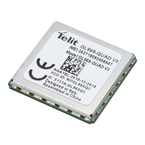
GL865 Hardware User Guide 1vv0300910 Rev.3 – 2011-10-03 GL865 Mechanical Dimensions The GL865 overall dimensions are: • Length: 24.4 mm • Width: 24.4 mm • Thickness: 2.7 mm • Weight 2.48 g Reproduction forbidden without Telit Communications S.p.A. written authorization - All Rights Reserved page 11 of 71... -
Page 12: Gl865 Module Connections
GL865 Hardware User Guide 1vv0300910 Rev.3 – 2011-10-03 GL865 module connections 4.1. PIN-OUT Signal Function Note Type Audio EAR- Earphone signal output, phase - Audio EAR+ Earphone signal output, phase + Audio MIC- Mic.signal input; phase- Audio MIC+ Mic.signal input; phase+ Audio AGND Analog Ground... - Page 13 GL865 Hardware User Guide 1vv0300910 Rev.3 – 2011-10-03 Signal Function Note Type Antenna output – 50 Ω Antenna GPIO GPIO01 Configurable GPIO GPIO_01 / DVI_WA0 CMOS 2.8V / Digital Audio Interface (WA0) GPIO_02 / JDR / GPIO02 Configurable GPIO / Jammer Detect Report CMOS 2.8V DVI_RX / Digital Audio Interface (RX)
- Page 14 GL865 Hardware User Guide 1vv0300910 Rev.3 – 2011-10-03 If not used, almost all pins should be left disconnected. The only exceptions are the following pins: signal 38, 37 VBATT & VBATT_PA 32, 33, 35, 36, 46 AGND V_AUX / PWRMON RESET* TX_AUX RX_AUX...
-
Page 15: Pin Layout
GL865 Hardware User Guide 1vv0300910 Rev.3 – 2011-10-03 4.2. Pin Layout TOP VIEW NOTE: The pin defined as NC/RFU has to be considered RESERVED and don’t connect on any pin in the application. Reproduction forbidden without Telit Communications S.p.A. written authorization - All Rights Reserved page 15 of 71... -
Page 16: Hardware Commands
GL865 Hardware User Guide 1vv0300910 Rev.3 – 2011-10-03 Hardware Commands 5.1. Auto-Turning ON the GL865 To Auto-turn on the GL865, the power supply must be applied on the power pins VBATT and VBATT_PA, after 1000 m-seconds, the pin will be at the high logic level V_AUX / PWRMON and the module can be consider fully operating. - Page 17 GL865 Hardware User Guide 1vv0300910 Rev.3 – 2011-10-03 NOTE: The power supply on the pins VBATT and VBATT_PA must be applied at the same time or for the special application in the first apply the VBATT_PA and in second time apply VBATT, never vice versa in this case can be damage the unit.
-
Page 18: Turning Off The Gl865
GL865 Hardware User Guide 1vv0300910 Rev.3 – 2011-10-03 5.2. Turning OFF the GL865 Turning off of the device can be done in two ways: • General turn OFF • Processor turn OFF General turn OFF – disconnect the power supply from the both power pins VBATT and VBATT_PA at the same time. - Page 19 GL865 Hardware User Guide 1vv0300910 Rev.3 – 2011-10-03 Modem OFF Proc. Disconnect PWR PWRMON = OFF? supply Place AT command AT#SYSHALT Wait PWRMON =OFF 15s timeout Disconnect PWR Modem ON Proc. Delay 1.5s supply TIP: To check if the device has been powered off, the hardware line PWRMON must be monitored. The device is powered off when PWRMON goes low.
-
Page 20: Resetting The Gl865
GL865 Hardware User Guide 1vv0300910 Rev.3 – 2011-10-03 5.3. Resetting the GL865 5.3.1. Hardware Unconditional restart WARNING: The hardware unconditional Restart must not be used during normal operation of the device since it does not detach the device from the network. It shall be kept as an emergency exit procedure to be done in the rare case that the device gets stacked waiting for some network or SIM responses. - Page 21 GL865 Hardware User Guide 1vv0300910 Rev.3 – 2011-10-03 In the following flow chart is detailed the proper restart procedure: Modem Reset Proc. Reset = LOW Delay 200ms Reset = HIGH Disconnect PWR Modem ON PWRMON = Delay 1,5s supply Proc. Start AT CMD.
-
Page 22: Power Supply
GL865 Hardware User Guide 1vv0300910 Rev.3 – 2011-10-03 Power Supply The power supply circuitry and board layout are a very important part in the full product design and they strongly reflect on the product overall performances, hence read carefully the requirements and the guidelines that will follow for a proper design. -
Page 23: General Design Rules
GL865 Hardware User Guide 1vv0300910 Rev.3 – 2011-10-03 GL 865 Average Mode Mode description (mA) SWITCHED OFF Module power supplied only on VBATT_PA pin, the VBATT pin Typical 2uA is not power supplied. Switched Off max 20uA Switched Off with Module power supplied on VBATT_PA pin and VBATT pin, the at <650uA AT#SYSHALT... -
Page 24: Electrical Design Guidelines
GL865 Hardware User Guide 1vv0300910 Rev.3 – 2011-10-03 • the thermal design • the PCB layout. 6.3.1. Electrical Design Guidelines The electrical design of the power supply depends strongly from the power source where this power is drained. We will distinguish them into three categories: •... - Page 25 GL865 Hardware User Guide 1vv0300910 Rev.3 – 2011-10-03 An example of linear regulator with 5V input is: 6.3.1.2. + 12V input Source Power Supply Design Guidelines The desired output for the power supply is 3.8V, hence due to the big difference between the input source and the desired output, a linear regulator is not suited and shall not be used.
- Page 26 GL865 Hardware User Guide 1vv0300910 Rev.3 – 2011-10-03 6.3.1.3. Battery Source Power Supply Design Guidelines The desired nominal output for the power supply is 3.8V and the maximum voltage allowed is 4.2V, hence a single 3.7V Li-Ion cell battery type is suited for supplying the power to the Telit GL865 module.
- Page 27 GL865 Hardware User Guide 1vv0300910 Rev.3 – 2011-10-03 The three cells Ni/Cd or Ni/MH 3,6 V Nom. battery types or 4V PB types MUST NOT BE USED DIRECTLY since their maximum voltage can rise over the absolute maximum voltage for the GL865 and damage it. NOTE: DON'T USE any Ni-Cd, Ni-MH, and Pb battery types directly connected with GL865.
-
Page 28: Thermal Design Guidelines
GL865 Hardware User Guide 1vv0300910 Rev.3 – 2011-10-03 6.3.2. Thermal Design Guidelines The thermal design for the power supply heat sink should be done with the following specifications: See para 7.2 Power Consumption NOTE: The average consumption during transmissions depends on the power level at which the device is requested to transmit by the network. -
Page 29: Power Supply Pcb Layout Guidelines
GL865 Hardware User Guide 1vv0300910 Rev.3 – 2011-10-03 6.3.3. Power Supply PCB layout Guidelines As seen on the electrical design guidelines the power supply shall have a low ESR capacitor on the output to cut the current peaks and a protection diode on the input to protect the supply from spikes and polarity inversion. -
Page 30: Antenna
GL865 Hardware User Guide 1vv0300910 Rev.3 – 2011-10-03 Antenna The antenna connection and board layout design are the most important aspect in the full product design as they strongly affect the product overall performances, hence read carefully and follow the requirements and the guidelines for a proper design. 7.1. -
Page 31: Pcb Guidelines In Case Of Fcc Certification
GL865 Hardware User Guide 1vv0300910 Rev.3 – 2011-10-03 This line of transmission shall fulfill the following requirements: ANTENNA LINE ON PCB REQUIREMENTS 50 ohm Impedance 0,3 dB Max Attenuation No coupling with other signals allowed Cold End (Ground Plane) of antenna shall be equipotential to the GL865 ground pins This transmission line should be designed according to the following guidelines: •... -
Page 32: Transmission Line Measurements
GL865 Hardware User Guide 1vv0300910 Rev.3 – 2011-10-03 possible. A Grounded Coplanar Waveguide (G-CPW) line has been chosen, since this kind of transmission line ensures good impedance control and can be implemented in an outer PCB layer as needed in this case. A SMA female connector has been used to feed the line. The interface board is realized on a FR4, 4-layers PCB. - Page 33 GL865 Hardware User Guide 1vv0300910 Rev.3 – 2011-10-03 Reproduction forbidden without Telit Communications S.p.A. written authorization - All Rights Reserved page 33 of 71...
- Page 34 GL865 Hardware User Guide 1vv0300910 Rev.3 – 2011-10-03 Line input impedance (in Smith Chart format, once the line has been terminated to 50 Ω load) is shown in the following figure: Insertion Loss of G-CPW line plus SMA connector is shown below: Reproduction forbidden without Telit Communications S.p.A.
-
Page 35: Gsm Antenna - Installation Guidelines
GL865 Hardware User Guide 1vv0300910 Rev.3 – 2011-10-03 7.3. GSM Antenna - Installation Guidelines • Install the antenna in a place covered by the GSM signal. • The Antenna must be installed to provide a separation distance of at least 20 cm from all persons and must not be co-located or operating in conjunction with any other antenna or transmitter;... -
Page 36: Logic Level Specifications
GL865 Hardware User Guide 1vv0300910 Rev.3 – 2011-10-03 Logic level specifications Where not specifically stated, all the interface circuits work at 2.8V CMOS logic levels. The following table shows the logic level specifications used in the GL865 interface circuits: Absolute Maximum Ratings -Not Functional Parameter Input level on any digital pin (CMOS -0.3V... -
Page 37: Reset Signal
GL865 Hardware User Guide 1vv0300910 Rev.3 – 2011-10-03 8.1. Reset signal Signal Function RESET* Phone reset RESET* is used to reset the GL865. Whenever this signal is pulled low, the GL865 is reset. When the device is reset it stops any operation. After the release of the reset GL865 is unconditionally shut down, without doing any detach operation from the network where it is registered. -
Page 38: Serial Ports
GL865 Hardware User Guide 1vv0300910 Rev.3 – 2011-10-03 Serial Ports The serial port on the GL865 is the core of the interface between the module and OEM hardware. 2 serial ports are available on the module: MODEM SERIAL PORT 1 (MAIN) for AT commands and Data MODEM SERIAL PORT 2 (AUX) ... - Page 39 GL865 Hardware User Guide 1vv0300910 Rev.3 – 2011-10-03 Output from the GL865 that indicates the DCD - dcd_uart Data Carrier Detect carrier presence RXD - tx_uart Transmit line *see Note Output transmit line of GL865 UART TXD - rx_uart Receive line *see Note Input receive of the GL865 UART Input to the GL865 that controls the DTE DTR - dtr_uart...
-
Page 40: Rs232 Level Translation
GL865 Hardware User Guide 1vv0300910 Rev.3 – 2011-10-03 9.2. RS232 level translation In order to interface the GL865 with a PC com port or a RS232 (EIA/TIA-232) application a level translator is required. This level translator must: • invert the electrical signal in both directions; •... - Page 41 GL865 Hardware User Guide 1vv0300910 Rev.3 – 2011-10-03 An example of level translation circuitry of this kind is: The example is done with a MAXIM MAX3237 Transceiver that could accept supply voltages of 3V DC. Not exceeded with supply voltage higher then 3.1VDC because this is the higher voltage limit of module’s inputs.
- Page 42 GL865 Hardware User Guide 1vv0300910 Rev.3 – 2011-10-03 Second solution could be done using a MAXIM transceiver (MAX218) In this case the compliance with RS232 (+-5V) is possible. Another level adapting method could be done using a standard RS232 Transceiver (MAX3237EAI) adding some resistors to adapt the levels on the GL865 Input lines.
-
Page 43: Uart Level Translation
GL865 Hardware User Guide 1vv0300910 Rev.3 – 2011-10-03 9.4. 5V UART level translation If the OEM application uses a microcontroller with a serial port (UART) that works at a voltage different from 2.8 - 3V, then a circuitry has to be provided to adapt the different levels of the two set of signals. - Page 44 GL865 Hardware User Guide 1vv0300910 Rev.3 – 2011-10-03 In case of reprogramming of the module has to be considered the use of the RESET line to start correctly the activity. The preferable configuration is having an external supply for the buffer. NOTE: In order to avoid a back powering effect it is recommended to avoid having any HIGH logic level signal applied to the digital pins of the GL865 when the module is powered OFF or during...
-
Page 45: Audio Section Overview
GL865 Hardware User Guide 1vv0300910 Rev.3 – 2011-10-03 Audio Section Overview The Base Band Chip of the GL865 provides one input for audio to be transmitted (Uplink), that can be connected directly to a microphone or an audio source. The bias for the microphone is already provided by the product; so the connection can be done in both following ways: For more information refer to Telit document : “... - Page 46 GL865 Hardware User Guide 1vv0300910 Rev.3 – 2011-10-03 TIP: Since the J-FET transistor inside the microphone acts as RF-detector-amplifier, ask vendor for a microphone with anti-EMI capacitor (usually a 33pF or a 10pF capacitor placed across the output terminals inside the case). LINE-IN connection Vmic 220n...
- Page 47 GL865 Hardware User Guide 1vv0300910 Rev.3 – 2011-10-03 EAR connection connection EAR+ OUTPUT EAR- MODULE The audio output of the GL865 is balanced, this is helpful to double the level and to reject common mode (click and pop are common mode and therefore rejected). These outputs can drive directly a small loudspeaker with electrical impedance not lower than 8Ohm.
-
Page 48: Electrical Characteristics
GL865 Hardware User Guide 1vv0300910 Rev.3 – 2011-10-03 10.1. Electrical Characteristics 10.1.1. Input Lines Microphone/Line-in path Line Type Differential ≥ 1μF Coupling capacitor 1kΩ/2kΩ/2.2kΩ Differential input resistance Levels To have 0dBm0 @1KHz Differential input voltage AT#HFMICG=0 290mVrms AT#HFMICG=1 (+6dB) 145mVrms AT#HFMICG=2 (+12dB) 72mVrms... -
Page 49: Output Lines
GL865 Hardware User Guide 1vv0300910 Rev.3 – 2011-10-03 10.1.2. Output Lines EAR/Line-out Output Direct connection (V =1.3÷1.6V) Differential line coupling One EAR terminal connected via a Single-ended line coupling DC-block capacitor, the other one left open ≥ 8 Ω output load resistance 4 Ω... -
Page 50: General Purpose I/O
GL865 Hardware User Guide 1vv0300910 Rev.3 – 2011-10-03 General Purpose I/O The general purpose I/O pads can be configured to act in three different ways: • input • output • alternate function ( internally controlled Input pads can only be read; they report the digital value ( ) present on the pad at the high or low read time . -
Page 51: Gpio Logic Levels
GL865 Hardware User Guide 1vv0300910 Rev.3 – 2011-10-03 current Reset Alternate function CMOS GPO_A Configurable GPO 1uA/1mA INPUT C109/DCD 2.8V Alternate function CMOS GPO_B Configurable GPO 1uA/1mA INPUT 2.8V C125/RING Alternate function CMOS GPO_C Configurable GPO 1uA/1mA INPUT 2.8V C107/DSR Alternate function CMOS GPI_E... -
Page 52: Using Agpio Pad As Output
GL865 Hardware User Guide 1vv0300910 Rev.3 – 2011-10-03 If the digital output of the device to be connected with the GPIO input pad has interface levels different from the 2.8V CMOS, then it can be buffered with an open collector transistor with a 47K pull up to 2.8V. -
Page 53: Using The Alarm Output Gpio6
GL865 Hardware User Guide 1vv0300910 Rev.3 – 2011-10-03 11.6. Using the Alarm Output GPIO6 The GPIO6 pad, when configured as Alarm Output, is controlled by the GL865 module and will rise when the alarm starts and fall after the issue of a dedicated AT command. This output can be used to controlling microcontroller or application at the alarm time. -
Page 54: Frequency Behaviour
GL865 Hardware User Guide 1vv0300910 Rev.3 – 2011-10-03 A magnetic Buzzer is a sound-generating device with a coil located in the magnetic circuit consisting of a permanent magnet, an iron core, a high permeable metal disk and a vibrating diaphragm. Drawing of the Magnetic Buzzer. -
Page 55: Working Current Influence
GL865 Hardware User Guide 1vv0300910 Rev.3 – 2011-10-03 Because resonance frequency depends on acoustic design, by lowering the amplitude of the driving signal the response bandwidth tends to become narrow, and vice versa. ↑ f ↓ ↓ f ↑ Summarizing: The risk is that the f could easily fall outside of new bandwidth;... - Page 56 GL865 Hardware User Guide 1vv0300910 Rev.3 – 2011-10-03 NOTE: Don’t use the STAT LED function if the GPIO 8 function is enabled and vice versa! A schematic example could be: Reproduction forbidden without Telit Communications S.p.A. written authorization - All Rights Reserved page 56 of 71...
-
Page 57: Simin Detect Function
GL865 Hardware User Guide 1vv0300910 Rev.3 – 2011-10-03 11.10. SIMIN detect function All the GPIO pins can be used as SIM DETECT input. The AT Command used to enable the function is: #SIMINCFG– SIMIN pin configuration SELINT 2 AT#SIMINCFG = <GPIO_ pin> The command enable the function on the general purpose I/O pin GPIO<pin>... -
Page 58: Rtc Bypass Out
GL865 Hardware User Guide 1vv0300910 Rev.3 – 2011-10-03 11.11. RTC Bypass out The VRTC pin brings out the Real Time Clock supply, which is separate from the rest of the digital part, allowing having only RTC going on when all the other parts of the device are off. To this power output a backup battery can be added in order to increase the RTC autonomy during power off of the main battery (power supply). -
Page 59: Dac And Adc Section
GL865 Hardware User Guide 1vv0300910 Rev.3 – 2011-10-03 DAC and ADC section 12.1. DAC Converter 12.1.1. Description The GL865 provides a Digital to Analog Converter. The signal (named DAC_OUT) is available on pin 15 of the GL865. The on board DAC is a 10 bit converter, able to generate a analogue value based a specific input in the range from 0 up to 1023. -
Page 60: Enabling Dac
GL865 Hardware User Guide 1vv0300910 Rev.3 – 2011-10-03 12.1.2. Enabling DAC An AT command is available to use the DAC function. The command is: AT#DAC= [<enable> [, <value>]] <value> - scale factor of the integrated output voltage (0..1023 - 10 bit precision) it must be present if <enable>=1 Refer to SW User Guide or AT Commands Reference Guide for the full description of this function. -
Page 61: Adc Converter
GL865 Hardware User Guide 1vv0300910 Rev.3 – 2011-10-03 12.2. ADC Converter 12.2.1. Description The on board A/D are 11-bit converter. They are able to read a voltage level in the range of 0÷2 volts applied on the ADC pin input, store and convert it into 11 bit word. Units Input Voltage range Volt... -
Page 62: Debug Of The Gl865 In Production
GL865 Hardware User Guide 1vv0300910 Rev.3 – 2011-10-03 12.3. Debug of the GL865 in production To test and debug the mounting of the GL865, we strongly recommend to foreseen test pads on the host PCB, in order to check the connection between the GL865 itself and the application and to test the performance of the module connecting it with an external computer. -
Page 63: Mounting The Gl865 On Your Board
GL865 Hardware User Guide 1vv0300910 Rev.3 – 2011-10-03 Mounting the GL865 on your Board 13.1. General The GL865 modules have been designed in order to be compliant with a standard lead-free SMT process. 13.2. Module finishing & dimensions Bottom View Pin 1 Lead-free Alloy: Surface finishing Ni/Au for all solder pads... -
Page 64: Recommended Foot Print For The Application
GL865 Hardware User Guide 1vv0300910 Rev.3 – 2011-10-03 13.3. Recommended foot print for the application Top View In order to easily rework the GE865 is suggested to consider on the application a 1.5 mm placement inhibit area around the module. It is also suggested, as common rule for an SMT component, to avoid having a mechanical part of the application in direct contact with the module. -
Page 65: Solder Paste
GL865 Hardware User Guide 1vv0300910 Rev.3 – 2011-10-03 13.4. Solder paste Lead free Sn/Ag/Cu Solder paste We recommend to use only “no clean” solder paste in order to avoid the cleaning of the modules after assembly 13.4.1. GL865 Solder reflow The following is the recommended solder reflow profile Reproduction forbidden without Telit Communications S.p.A. - Page 66 GL865 Hardware User Guide 1vv0300910 Rev.3 – 2011-10-03 Profile Feature Pb-Free Assembly Average ramp-up rate (T to T 3°C/second max Preheat – Temperature Min (Tsmin) 150°C – Temperature Max (Tsmax) 200°C – Time (min to max) (ts) 60-180 seconds Tsmax to TL –...
-
Page 67: Packing System
GL865 Hardware User Guide 1vv0300910 Rev.3 – 2011-10-03 Packing system The GL865 modules are packaged on trays of 20 pieces each. This is especially suitable for the GL865 according to SMT processes for pick & place movement requirements. NOTE: All temperatures refer to topside of the package, measured on the package body surface WARNING: These trays can withstand at the maximum temperature of 65°... -
Page 68: Moisture Sensibility
GL865 Hardware User Guide 1vv0300910 Rev.3 – 2011-10-03 14.1. Moisture sensibility The level of moisture sensibility of the Product is “3”, according with standard IPC/JEDEC J- STD-020, take care of all the relative requirements for using this kind of components. Moreover, the customer has to take care of the following conditions: a) The shelf life of the Product inside of the dry bag must be 12 months from the bag seal date, when stored in a non-condensing atmospheric environment of <40°C / 90% RH... -
Page 69: Conformity Assessment Issues
GL865 Hardware User Guide 1vv0300910 Rev.3 – 2011-10-03 Conformity Assessment Issues The Telit GL865 Module has been assessed in order to satisfy the essential requirements of the R&TTE Directive 1999/05/EC (Radio Equipment & Telecommunications Terminal Equipments) to demonstrate the conformity against the harmonised standards with the final involvement of a Notified Body. -
Page 70: Safety Recommandations
GL865 Hardware User Guide 1vv0300910 Rev.3 – 2011-10-03 SAFETY RECOMMANDATIONS READ CAREFULLY Be sure the use of this product is allowed in the country and in the environment required. The use of this product may be dangerous and has to be avoided in the following areas: •... -
Page 71: Document History
GL865 Hardware User Guide 1vv0300910 Rev.3 – 2011-10-03 Document History Rev.0 2011-01-05 First ISSUE Rev.1 2011-03-10 VBATT_PA power consumption specification Page 18 typical 2uA max 20uA Page 23 typical 2uA max 20uA AUX serial port naming from RXD_AUX; TXD_AUX to RX_AUX; TX_AUX Rev.2 2011-08-24 Added chapter 7.2 PCB guidelines in case of FCC certifications –...
Need help?
Do you have a question about the GL865 QUAD and is the answer not in the manual?
Questions and answers