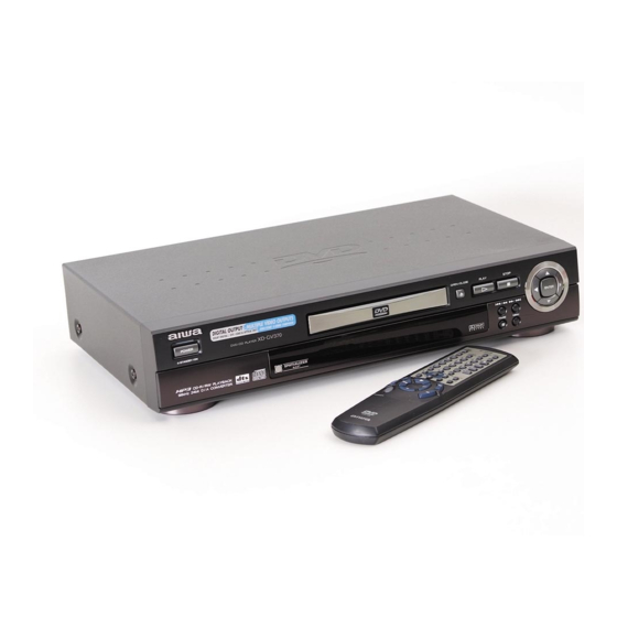
Aiwa XD-DV370 Service Manual
Hide thumbs
Also See for XD-DV370:
- Operating instructions manual (50 pages) ,
- Operating instructions manual (48 pages) ,
- Operating instructions manual (48 pages)
Table of Contents
Advertisement
<HR(N)>
SERVICE MANUAL
DVD PLAYER
If requiring information about the ELECTRICAL ADJUSTMENT & MECHANSIM
ADJUSTMENT & MECHANISM PARTS LOCATION <EZ> & MECHANISM DISASSEMBLY
<EZ> & FL GRID ASSINGMENT/ANODE CONNECTION/PIN CONNECTION.
see Supplement Service manual of XD-DV370(HR/U/K/EZ) (S/M Code No. 09-00C-349-9S1)
XD-DV370
BASIC DVD/CD MECHANISM :
S/M Code No. 09-009-349-9N1
HR(N) EZ(N, B) K(N)
U(B)
<Except for HR(N)>
DP2[6721R-0308A](HR/K/U)
DP3[6721R-0309A](EZ)
Advertisement
Table of Contents

Subscribe to Our Youtube Channel
Related Manuals for Aiwa XD-DV370


Summary of Contents for Aiwa XD-DV370
- Page 1 DP3[6721R-0309A](EZ) If requiring information about the ELECTRICAL ADJUSTMENT & MECHANSIM ADJUSTMENT & MECHANISM PARTS LOCATION <EZ> & MECHANISM DISASSEMBLY <EZ> & FL GRID ASSINGMENT/ANODE CONNECTION/PIN CONNECTION. see Supplement Service manual of XD-DV370(HR/U/K/EZ) (S/M Code No. 09-00C-349-9S1) S/M Code No. 09-009-349-9N1...
-
Page 2: Table Of Contents
TABLE OF CONTENTS SPECIFICATIONS ................................... 3 PROTECTION OF EYES FROM LASER BEAM DURING SERVING .................... 4 ACCESSORIES LIST ..................................5 DISASSEMBLY INSTRUCTIONS ............................. 6 ~ 7 ELECTRICAL MAIN PARTS LIST ............................8 ~ 10 TRANSISTOR ILLUSTRATION ..............................11 BLOCK DIAGRAM - 1 (OVERALL) <HR> ............................. 12 BLOCK DIAGRAM - 2 (OVERALL) <Except HR>... -
Page 3: Specifications
SPECIFICATIONS <U MODEL> <HR, EZ, K MODELS> Power supply 120 V AC, 60 Hz Power supply 110 - 240 V AC, 50/60 Hz <HR, EZ> Power consumption 16 W 230 V AC, 50 Hz <K> Weight 3.2 kg (7.1 lbs) Power consumption 16 W External dimensions 430 ×... -
Page 4: Protection Of Eyes From Laser Beam During Servicing
PROTECTION OF EYES FROM LASER BEAM DURING SERVICING CAUTION This set employs laser. Therefore, be sure to follow carefully the instructions below when servicing. Use of controls or adjustments or performance of proce- dures other than those specified herin may result in WARNING! hazardous radiation exposure. -
Page 5: Accessories List
ACCESSORIES LIST REF. NO PART NO. KANRI DESCRIPTION 1 S8-35R-S00-12X INSTRUCTION ASSY<HRN> 1 S8-35R-S00-12W INSTRUCTION ASSY<UB> 1 S8-35R-S00-12V INSTRUCTION ASSY<KN> 1 S8-35R-S00-12Z INSTRUCTION ASSY<EZB,EZN> 2 S7-11R-2N0-13F REMOTE CONTROLLER ASSY<HRN> 2 S7-11R-2N0-13D REMOTE CONTROLLER ASSY<UB,EZB> 2 S7-11R-2N0-13E REMOTE CONTROLLER ASSY<KN,EZN> 3 S5-640-17B-000 PLUG ASSY PHONE CORD 1WAY 3 S5-640-18B-000 PLUG ASSY PHONO CORD... -
Page 6: Disassembly Instructions
DISASSEMBLY -1/2 CABINET DISASSEMBLY 3. Front Panel 1. Eject the disc tray. (See Fig. 2-2) 1. Top Case 2. Remove the tray door. (See Fig. 2-2) 1. Release 7 screws (A). (See Fig. 2-1) 3. Release 2 screws (B). 2. Lift the top case with holding the back of it, 4. -
Page 7: Circuit Board Disassembly
DISASSEMBLY -2/2 CIRCUIT BOARD DISASSEMBLY 1. Disassembling of Main Circuit Board and Interface Board 2. Key1 and Key2 Circuit Board 1. Remove the top case.(See Fig. 2-1) 1. Remove the front panel.(See Fig. 2-3) 2. Remove 12 screw (C). 2. Release 4 screws (E), and remove the Key1, 2 3. -
Page 8: Electrical Main Parts List - 1/3
ELECTRICAL MAIN PARTS LIST - 1/3 REF. NO PART NO. KANRI DESCRIPTION REF. NO PART NO. KANRI DESCRIPTION C272 SC-H84-76C-611 C-CAP,47UF-6.3V C274 SC-H84-76C-611 C-CAP,47UF-6.3V ! ! ! ! ! SI-SK6-153-00A IC,STR-G6153T 5P<EXCEPT U> C275 SC-H71-06C-611 C-CAP,10UF-6.3V S2-309-024-040 SENSORLTV-817B PHOTO COU C276 SC-H71-06C-611 C-CAP,10UF-6.3V... - Page 9 ELECTRICAL MAIN PARTS LIST - 2/3 REF. NO PART NO. KANRI DESCRIPTION REF. NO PART NO. KANRI DESCRIPTION PMD02 S6-30R-FB0-2W0 CONN,04-6232-123-008-80 F602 S2-00H-JC9-01A SAM,FILTER CFI06B1H101MF<EXCEPT HR> PMD03 S6-30R-FB0-2H0 CONN,04-6232-108-008-800 F603 S2-00H-JC9-01A SAM,FILTER CFI06B1H101MF PMD04 S6-30R-3S0-06F CONN,5P F604 S2-00H-JC9-01A SAM,FILTER CFI06B1H101MF X301 S2-02R-BL0-1A0 X'TAL,HC-49/SM5H...
-
Page 10: Electrical Main Parts List
ELECTRICAL MAIN PARTS LIST - 3/3 REF. NO PART NO. KANRI DESCRIPTION ZD639 SD-Z56-260-9AA ZENER,GDZJ5.6B 26MM TP<K,EZ> ZD640 SD-Z56-260-9AA ZENER,GDZJ5.6B 26MM TP<K,EZ> KEY1 C.B P9901 S5-636-02R-000 CONN,4P SW901 S5-562-19B-000 SW,SKHV10910B KEY2 C.B P9903 S5-636-02S-000 CONN,12P SW902 S5-562-19B-000 SW,SKHV10910B SW903 S5-562-19B-000 SW,SKHV10910B SW904 S5-562-19B-000... -
Page 11: Transistor Illustration
TRANSISTOR ILLUSTRATION E C B E C B E C B KTA1015 KTA1266 KSB1151 2SA1037 KTC103 KTC3198 2SC2412 KTC1015 DTC124EK KTA1504 KTA1505 B C E UMZ1N 3K KTC4419 -11-... -
Page 22: Wire Harness Diagram
WIRE HARNESS DIAGRAM P3901 DOWNLOAD KEY 1 C.B KEY 2 C.B 16:9 DVD MECHA. P5901 PICK UP CB INTERFACE MAIN C.B ECH_VOL MIC_ON DVD MECHA. LOADING MOTOR C.B DVD MECHA. SPINDLE MOTOR C.B -22-... -
Page 23: Schematic Diagram - 1 (Main -1/5, Audio Section)
SCHEMATIC DIAGRAM - 1 (MAIN -1/5, AUDIO SECTION) MAIN-1/5 (AUDIO SECTION) C.B PQ20WZ5U HB-1M2012-102JT MAIN-5/5 (MAIN u-COM) E1-E8 47UF/6.3V HB-1M2012-102JT 100UF/16V 47UF/6.3V (1/3) MAIN-4/5 (1/3) (MPEG) (1/3) D1-D19 (3/3) 47UF/6.3V 47UF/6.3V (3/3) (3/3) <HRJNK> MPEG SECTION L1-L3 MAIN-5/5 (MAIN u-COM) R3,R8 <HRJNK>... -
Page 24: Schematic Diagram - 2 (Main -2/5, Drive & Rf Section)
SCHEMATIC DIAGRAM - 2 (MAIN -2/5, DRIVE & RF SECTION) DVD MECHA. PICK UP CB MAIN-2/5 (DRIVE & RF SECTION) C.B MAIN-3/5 (DVD DSP) HB-1M2012-102JT (3/3) MAIN-5/5 (MAIN u-COM) H11-H13 MAIN-5/5 (MAIN u-COM) R1-R3,R5,R8 7.5K (1/3) 5.6K SSI33P3721 MAIN-3/5 MOTOR DRIVE (DVD DSP) RF SIGNAL G8-G13... -
Page 25: Schematic Diagram - 3 (Main -3/5, Dvd Dsp Section)
SCHEMATIC DIAGRAM - 3 (MAIN -3/5, DVD DSP SECTION) MAIN-3/5 (DVD DSP SECTION) C.B IC205 GLT441L16 DRAM MAIN-5/5 10UF/6.3V (MAIN u-COM) F1-F37 (2/3) (2/3) IC201 GDC25D801C MAIN-5/5 (MAIN u-COM) CD/DVD DSP (3/3) R5,R7,R8 DVD SERVO (2/4) MAIN-2/5 (DRIVE & RF) (1/3) G1-G19 (4/4) -
Page 26: Schematic Diagram - 4 (Main -4/5, Mpeg Section)
SCHEMATIC DIAGRAM - 4 (MAIN -4/5, MPEG SECTION) <HR> MAIN-4/5 (MPEG SECTION) C.B <HR> INTERFACE-1/3 C.B (JACK) P6401 MAIN-3/5 (DVD DSP) K1-K12 ZIVA3-P MPEG A/V DECODER (3/3) (2/3) VIDEO ENCODER MAIN-1/5 (AUDIO) D1-D19 (1/3) MAIN-5/5 (MAIN u-COM) C1-C27 MAIN-1/5 (3/3) (AUDIO) SDRAM SDRAM... -
Page 27: Schematic Diagram - 5 (Main -4/5, Mpeg Section)
SCHEMATIC DIAGRAM - 5 (MAIN -4/5, MPEG SECTION) <Except HR> MAIN-4/5 (MPEG SECTION) C.B <U, K, EZ> INTERFACE-1/3 C.B (JACK) P6401 MAIN-3/5 (DVD DSP) K1-K12 (2/3) (1/3) (2/3) MPEG A/V DECODER (3/3) (2/3) (3/3) SWITCH MAIN-1/5 (AUDIO) D1-D17 6.3V 6.3V (1/3) 6.3V (3/3) -
Page 28: Schematic Diagram - 6 (Main -5/5, Main Μ-Com Section)
SCHEMATIC DIAGRAM - 6 (MAIN -5/5, MAIN µ-COM SECTION) MAIN-5/5 (MAIN u-COM SECTION) C.B MAIN-2/5 (DRIVE & RF) H1-H13 (1/5) (1/5) (1/4) EXPANDER (4/4) (1/6) AT49F8192A FLASH ROM DRAM (6/6) (1/3) (2/6) DOWNLOAD MAIN-1/5~4/5 (AUDIO, DRIVE & RF, (3/4) DVD DSP, MPEG) MAIN-3/5 R1-R8... -
Page 29: Wiring - 1 (Main C.b)
WIRING - 1 (MAIN C.B) <HR> P3901 INTERFACE C.B MAIN C.B <HR> P6401 P5502 P5901 PMD04 PMD02 PMD03 DOWN LOAD INTERFACE C.B DVD MECHA. DVD MECHA. DVD MECHA. P9501 LOADING PICK UP C.B SPINDLE MOTOR C.B MOTOR C.B -29-... -
Page 30: Wiring - 2 (Main C.b)
WIRING - 2 (MAIN C.B) <Except HR> P3901 MAIN C.B <U, K, EZ> INTERFACE C.B P6401 10 14 4548 P5502 P5901 PMD04 PMD02 PMD03 DOWN LOAD INTERFACE C.B DVD MECHA. DVD MECHA. DVD MECHA. P9501 LOADING PICK UP C.B SPINDLE MOTOR C.B MOTOR C.B -30-... -
Page 31: Schematic Diagram - 7 (Interface - 1/3, Timer Section) (Key1, Key2 Section)
SCHEMATIC DIAGRAM - 7 (INTERFACE - 1/3, TIMER SECTION) (KEY1, KEY2 SECTION) <HR> INTERFACE-2/3 (TIMER SECTION) C.B <HR> KEY2 C.B KEY1 C.B SW904 SW903 SW902 STOP PLAY OPEN/CLOSE 7-BT-273GN STANDBY/ON SW905 SW907 SW906 MENU SW908 SW911 SW913 SW914 SW912 SW910 ENTER LC866112B-5N21 FRONT CONTROL... -
Page 32: Schematic Diagram - 8 (Interface - 1/3, Timer Section) (Key1, Key2 Section)
SCHEMATIC DIAGRAM - 8 (INTERFACE - 1/3, TIMER SECTION) (KEY1, KEY2 SECTION) <Except HR> INTERFACE-1/3 (TIMER SECTION) C.B <U, K, EZ> KEY2 C.B KEY1 C.B SW904 SW903 SW902 STOP PLAY OPEN/CLOSE 7-BT-273GN STANDBY/ON SW907 SW906 SW905 MENU SW908 SW913 SW911 SW912 SW914 SW910... -
Page 33: Schematic Diagram - 9 (Interface -2/3, Jack Section)
SCHEMATIC DIAGRAM - 9 (INTERFACE -2/3, JACK SECTION) <HR> INTERFACE-2/3 (JACK SECTION) C.B <HR> JK602 AUDIO COMPONENT AUDIO VIDEO OUT OUT2 S-VIDEO VIDEO DIGITAL DIGITAL R622 R6M2 R6M1 (1/3) (1/3) MAIN-4/5 C.B (MPEG) P3901 D603 C608 KTC3198 0.047UF D604 KTC3198 INTERFACE-1/3 (TIMER) B1-B10... -
Page 34: Schematic Diagram - 10 (Interface -2/3, Jack Section)
SCHEMATIC DIAGRAM - 10 (INTERFACE -2/3, JACK SECTION) <U> INTERFACE-2/3 (JACK SECTION) C.B <U> JK602 AUDIO COMPONENT AUDIO VIDEO OUT OUT2 DIGITAL S-VIDEO VIDEO DIGITAL R622 470U/10V R6M2 R6M1 (1/3) (1/3) MAIN-4/5 C.B 470U/10V (MPEG) P3901 D603 C608 KTC3198 0.047UF D604 KTC3198 INTERFACE-1/3... -
Page 35: Schematic Diagram - 11 (Interface - 2/3, Jack Section)
SCHEMATIC DIAGRAM - 11 (INTERFACE -2/3, JACK SECTION) <K, EZ> INTERFACE-2/3 (JACK SECTION) C.B <K, EZ> 21PIN SCART JK602 CONNECTOR AUDIO DIGITAL S-VIDEO VIDEO DIGITAL C6Z5 C6Z6 470U/10V 470U/10V R622 470U/10V C6Z4 470U/10V (2/3) 470U/10V KTA1266-GR MAIN-4/5 C.B 470U/10V (MPEG) P3901 D603 C608... -
Page 36: Schematic Diagram - 12 (Interface -3/3, Power Section)
SCHEMATIC DIAGRAM - 12 (INTERFACE -3/3, POWER SECTION) <U> INTERFACE-3/3 (POWER SECTION) C.B <U> TRANS 350V GDZJ5.6B GDZJ6.2B PQ3RD13 3.3V REG 275V PQ3RD13 3.3V REG 8V REG -10A (T/W) 470 /10V LTV-817B AC INPUT NTERFACE-1/3 (TIMER) A1-A17 NOTES) Warning NOTES) Parts that are shaded are critical NOTES) With respect to risk of fire or... -
Page 37: Schematic Diagram - 13 (Interface -3/3, Power Section)
SCHEMATIC DIAGRAM - 13 (INTERFACE -3/3, POWER SECTION) <Except U> INTERFACE-3/3 (POWER SECTION) C.B <HR, K, EZ> TRANS GDZJ5.6B 275V PQ3RD13 3.3V REG 275V 400V PQ3RD13 3.3V REG 8V REG -10A (1/2W) DRIVE & OVER CURRENT LIMIT LTV-817B AC INPUT NTERFACE-1/3 (TIMER) A1-A17... -
Page 38: Wiring - 3 (Interface C.b)
WIRING - 3 (INTERFACE C.B) <HR> COMPONENT S-VIDEO AUDIO VIDEO VIDEO OUT OUT2 AC INPUT INTERFACE C.B AUDIO SW601 DIGITAL <HR> NTSC AUTO JK601 DIGITAL P6401 MAIN C.B P3901 P9501 MAIN C.B P5901 P9904 VR803 VR802 VR801 P9902 DIGITAL MIC 2 MIC 1 KEY2 C.B RC901... -
Page 39: Wiring - 4 (Interface C.b)
WIRING - 4 (INTERFACE C.B) <U> COMPONENT S-VIDEO AUDIO VIDEO VIDEO OUT OUT2 AC INPUT AUDIO INTERFACE C.B <U> DIGITAL JK601 DIGITAL P6401 MAIN C.B P3901 E C B P9501 MAIN C.B P5901 P9904 KEY2 C.B RC901 DIG901 P9903 T/W:JUMPER WIRE (REMOCON RECEIVE) (DIGTRON) -39-... -
Page 40: Wiring - 5 (Interface C.b)
WIRING - 5 (INTERFACE C.B) <K, EZ> S-VIDEO VIDEO AC INPUT INTERFACE C.B JK603 AUDIO SW601 DIGITAL <K, EZ> 21PIN SCART NTSC AUTO CONNECTOR JK601 DIGITAL P6401 MAIN C.B P3901 P9501 MAIN C.B P5901 P9904 P9902 KEY2 C.B RC901 T/W:JUMPER WIRE DIG901 KEY1 C.B P9903... -
Page 41: Wiring - 6 (Key1, Key2 C.b)
WIRING - 6 (KEY1, KEY2 C.B) KEY1 C.B LED901 INTERFACE C.B SW901 P9902 POWER STANDBY/ON KEY2 C.B INTERFACE C.B P9904 SW912 SW903 SW904 SW902 SW913 SW911 SW910 SW914 SW906 SW905 SW907 SW908 SW902 SW904 SW903 SW912 STOP PLAY OPEN/CLOSE SW910 SW913 SW906 SW905... -
Page 42: Waveforms - 1/2
WAVEFORMS - 1/2 IC305 (VIDEO ENCODER) IC305 Pin30 Composite IC305 Pins 9 ~ 16 MPEG Data IC305 Pin24 Chrominance 1.0V/500µs 500mV/20µs 500mV/20µs M 500 s 280/mV 1.00V IC305 Pins 40,41 SDA/SCL IC305 Pin27 Luminance IC305 Pin4 MPEG Clock (27MHz) 500mV/20µs 1.0V/25ms 1.0V/500µs M 500 s... - Page 43 WAVEFORMS - 2/2 IC2A1, IC201 (RF/SERVO) IC2A1 Pin24 Focus Error IC2A1 Pin41 Tracing Error IC2A1 Pin41 VBR Tracking Error IC2A1 Pin36 Pi 500mV/2ms 500mV/300µs 500mV/5ms IC201 Pin88 SLED Driver (FMO) IC2A1 Pin57 RF IC2A1 Pin42 Focus Error(in Focus Search) 0.5V/0.1µs IC201 Pin18 SLED FG IC201 Pin83 Focus Drive (FDO) A: 2.0V/500ms, B: 500mV/500ms...
-
Page 44: Ic Block Diagram - 1/2
IC BLOCK DIAGRAM - 1/2 IC, PCM1716E BCKIN Low-pass Serial Filter LRCIN Input EXTL 8X Oversampling Enhanced Digital Filter with Multi-level Function Delta-Sigma Controller Modulator Low-pass Filter ML/IIS EXTR MC/DM1 MD/DM0 ZERO Mode CS/IWO Control BPZ-Cont. Open Drain MODE MUTE Crystal/OSC Power Supply CLKO... - Page 45 IC BLOCK DIAGRAM - 2/2 IC, PLL1700E MODE GNDP GNDB Mode Power Supply Control Reset PLL2 PLL1 Counter Q Counter P MCKO MCKO SCKO1 SCKO2 SCKO3 SCKO4 IC, XC9536_15VQ44C-PROG JTAG In-System Programming Controller JTAG Port Controller Function Block 1 Macrocells 1 to 18 Function Block 2...
-
Page 46: Ic Description
IC DESCRIPTION - 1/11 (SSI33P3721)-1/2 Pin No. Pin Name Description DVDRFP RF SIGNAL INPUTS: Differential RF signal attenuator input pins. DVDRFN CD PHOTO DETECTOR INTERFACE INPUTS: Inputs from the CD photo detector outputs. PHOTO DETECTOR NTERFACE INPUTS: AC coupled inputs for the DPD from the main beam Photo detector matrix outputs. - Page 47 IC DESCRIPTION - 1/11 (SSI33P3721)-2/2 Pin No. Pin Name Description PULL-IN SIGNAL OUTPUT: The summing signal output of A,B,C,D inputs for mirror detection. Reference to VCI. DEFECT OUTPUT: Pseudo CMOS output. When defect is detected, the DFT output goes high. Also the servo AGC output can be monitored at this DFT pin, when CAR bit7-4 is ‘0011’.
- Page 48 IC DESCRIPTION - 2/11 (KA3032)-1/1 Pin No. Pin Name Description OUT1 CH 1 op-amp output IN2.1 CH 1 op-amp input (+) IN2.2 CH 2 op-amp input (-) OUT2 CH 2 op-amp output IN3.1 CH 3 op-amp input (+) 6, 7 –...
- Page 49 IC DESCRIPTION - 3/11 (GLT441L16-40)-1/1 Pin No. Pin Name Description – Power Supply (+3.3 V) 2 ~ 5 DQ0 ~ DQ3 Data-In / Data-Out – Power Supply (+3.3 V) 7 ~ 10 DQ4 ~ DQ7 Data-In / Data-Out 11, 12 –...
- Page 50 IC DESCRIPTION - 4/11 (GM72V161621ET-7)-1/2 Pin No. Pin Name Description – 3.3 V is applied. (VCC is for the internal circuit.) Data is input and ouput from these pins. These pins are the same as those of a conventional DRAM. VSSQ –...
- Page 51 IC DESCRIPTION - 4/11 (GM72V161621ET-7)-2/2 Pin No. Pin Name Description This pin determines whether or not the next CLK is valid. If CKE is High, the next CLK rising edge is valid. If CKE is Low, the next CLK rising edge is invalid. This pin is used for power- down and clock suspend modes.
- Page 52 IC DESCRIPTION - 5/11(PLL1700E)-1/1 Pin No. Pin Name Description Latch Enable for Software Mode/Sampling Rate Selection for Hardware Mode. When MODE D PLL L pin is LOW, ML is selected.(1) Mode Control Select. When this pin is HIGH, device is operated in hardware mode using SR0 MODE (pin 1), FS0 (pin 19), and FS1 (pin 20).
- Page 53 IC DESCRIPTION - 6/11 (PCM1716E)-1/1 Pin No. Pin Name Description LRCIN Left and Right Clock Input. This clock is equal to the sampling rate - f .(1) Serial Audio Data Input. (1) BCKIN Bit Clock Input for Serial Audio Data.(1) CLKO Buffered Output of Oscillator.
- Page 54 IC DESCRIPTION - 7/11 (AT49F8192A-90TC)-1/1 Pin No. Pin Name Description 1 ~ 8 A16 ~ A9 Addresses Addresses – Not used _______ Write Enable ____________ RESET Reset 13 ~ 15 – Not used 16, 17 A18, A17 Addresses 18 ~ 25 A7 ~ A0 Addresses _____...
- Page 55 IC DESCRIPTION - 8/11 (V53C16256HK50)-1/1 Pin No. Pin Name Description – +5V Supply 2 ~ 5 D00 ~ D03 Data Input, Output – +5V Supply 7 ~ 10 D04 ~ D07 Data Input, Output 11, 12 – Not used ______ Write Enable ________ Row Address Strobe...
- Page 56 IC DESCRIPTION - 9/11(LC866112B-5N21)-1/2 Pin No. Pin Name Description ______ Select DOWN SW input from SW914 Enter SW input from SW910 Select right SW input SW911 PWM1 Not used. TEST1 – Not used. (TEST port) _______ Reset signal input from IC902 3pin Not used.
- Page 57 Pin No. Pin Name Description VFD display control signal output. DIG 901 P10 to P19 – – Not used. – – D902 option (Present at AIWA remocon model) – Not used. – – Diode option input – – Not used.
- Page 58 IC DESCRIPTION - 10/11(GDC25D801C)-1/5 Pin No. Pin Name Description DAT1 Bi-directional data to DRAM DAT2 Bi-directional data to DRAM DAT3 Bi-directional data to DRAM DAT4 Bi-directional data to DRAM DAT5 Bi-directional data to DRAM DAT6 Bi-directional data to DRAM DAT7 Bi-directional data to DRAM DAT8 Bi-directional data to DRAM...
- Page 59 IC DESCRIPTION - 10/11(GDC25D801C) - 2/5 Pin No. Pin Name Description TEST_OUT8 Test output (Not used) TEST_OUT7 Test output (Not used) TEST_OUT6 Test output (Not used) T_SEL Test mode selection TEST_OUT5 Test output (Not used) TEST_OUT4 Test output (Not used) TEST_OUT3 Test output (Not used) TEST_OUT2...
- Page 60 IC DESCRIPTION - 10/11(GDC25D801C) - 3/5 Pin No. Pin Name Description AVDD – Analog power supply for ADC AGND – Analog GND for ADC AOUT3 AOUT4 D_VREF DGND – Digital GND for ADC RFVCM – Analog GND for ADC AGND –...
- Page 61 IC DESCRIPTION - 10/11(GDC25D801C) - 4/5 Pin No. Pin Name Description SI_ENC1 SLED ENCODER1 INPUT SI_ENC2 SLED ENCODER2 INPUT TRACK CROSS PULSE 2 INPUT MIRR TRACK CROSS PULSE 1 INPUT MSDATAO SERVO DSP INTENAL STATUS SERIAL OUTPUT INTERNAL GENERATED FOK(Focus OK) H=OK –...
- Page 62 IC DESCRIPTION - 10/11(GDC25D801C) - 5/5 Pin No. Pin Name Description Spindle motor ON/OFF control signal LOCK CLV servo lock signal FG_M – Digital GND SCAN_OUT SCAN DATA OUTPUT (Not used) – Digital power supply Interrupt request to Host Read strobe from HOST Write strobe from HOST Chip select from HOST Internal register address from HOST...
- Page 63 IC DESCRIPTION - 11/11(ZIVA4.1) - 1/5 Pin No. Pin Name Description _____ Read strobe in I mode. Must be held HIGH in M Mode. ____ Read/write strobe in M mode. Write strobe in I mode. Host asserts R/W LOW to select Write and ____ LOW to select Read for M Mode only.
- Page 64 IC DESCRIPTION - 11/11(ZIVA4.1) - 2/5 Pin No. Pin Name Description 57 ~ 62 MDATA2 ~ MDATA7 SDRAM Data MDATA15 SDRAM Data VDD_3.3 – 3.3-V supply voltage for I/O signals. – Ground for core logic and I/O signals. MDATA14 SDRAM Data VDD_2.5 –...
- Page 65 IC DESCRIPTION - 11/11(ZIVA4.1) - 3/5 Pin No. Pin Name Description DAI-DATA PCM data input. 118 ~ 121 DA-DATA3~ DA-DATAO PCM Data Out. Eight channels. Serial audio samples relative to DA_BCK and DA_LRCK. DA-LRCK PCM Left Clock. Identifies the channel for each sample. The polarity is programmable. VDD_3.3 –...
- Page 66 IC DESCRIPTION - 11/11(ZIVA4.1) - 4/5 Pin No. Pin Name Description Video clock. Clocks out data on input. VDATA[7:0]. Clock is typically 27 MHz. VCLK System clock that drives internal PLLs and internal DENC. ZiVA-4 requires an external 27-MHz TTL oscillator. A_VDD –...
-
Page 67: Ic Description
IC DESCRIPTION - 11/11(ZIVA4.1) - 5/5 Pin No. Pin Name Description VDD_2.5 – 2.5-V supply voltage for core logic. RESERVED Tie to VSS or VDD_3.3. – Ground for core logic and I/O signals. VDD_3.3 – 3.3-V supply voltage for I/O signals. 193 ~ 196 RESERVED Tie to VSS or VDD_3.3. -
Page 68: Mechanical Exploded View 1/1
MECHANICAL EXPLODED VIEW 1/1 <EXCEPT FOR HR> <HR ONLY> -68-... -
Page 69: Mechanical Main Parts List 1/1
MECHANICAL MAIN PARTS LIST 1/1 REF. NO PART NO. KANRI DESCRIPTION 001 S9-30R-018-5A0 HOLDER DIGITRON 250 S1-10R-018-4G0 CASE TOP<HRN,KN,EZN> 250 S1-10R-018-4A0 CASE TOP<UB,EZB> ———— CHASSIS ASSY MAIN 275 S9-30R-018-3A0 HOLDER MAIN PCB 279 S9-30R-019-9A0 HOLDER CONNECTOR 280 S7-21R-F15-7B0 PANEL ASSY FRONT<HRN> 280 S7-21R-F15-7A0 PANEL ASSY FRONT<UB>... -
Page 70: Color Name Table
COLOR NAME TABLE COLOR NAME TABLE Basic color symbol Color Basic color symbol Color Basic color symbol Color Black Cream Orange Green Gray Blue Transparent Blue Gold Pink Silver Titan Silver Brown Violet White Transparent White Yellow Transparent Yellow Metallic Blue Light Blue Transparent Green Dark Blue... -
Page 71: Dvd Mechanism Exploded View 1/1
DVD MECHANISM EXPLODED VIEW 1/1 -71-... -
Page 72: Dvd Mechanism Main Parts List 1/1
DVD MECHANISM MAIN PARTS LIST 1/1 REF. NO PART NO. KANRI DESCRIPTION 001 S3-00R-054-7A0 PLATE CLAMP ———— CLAMP MAGNET 8,10-5,1-1.5 ———— CLAMP UPPER 004 S9-30R-017-1A0 HOLDER CLAMP 008 S4-70R-004-7A0 GEAR ASSY RACK<HRN,UB,KN> 008 S4-70R-008-0A0 GEAR ASSY, RACK<EZB,EZN> 009 S4-70R-005-3A0 GEAR MIDDLE<HRN,UB,KN> 009 S4-70R-007-9A0 GEAR MIDDLE<EZB,EZN>... - Page 73 ELECTRICAL TROUBLESHOOTING GUIDE -1/11 1. Power(SMPS) Circuit No 5V_D No VF+ or 5V_A . Is 5.2VA section working? Is 5.2VA section working? Is oscillation present at the Is oscillation present at the anode of D109? Base of Q108? No 5.2VA. Replace D109.
- Page 74 ELECTRICAL TROUBLESHOOTING GUIDE -2/11 2. µ-COM Circuit A. No Power POWER ON Does Bar appear at FLD? Is P5901 Do all five Bars appear? connected normally? Reconnect it. Does Logo appear Check power. on the screen? (Refer to power) If power is normal Is P5901 Pin 24 normal? Refer to Front Part...
- Page 75 ELECTRICAL TROUBLESHOOTING GUIDE -3/11 B. Audio abnormal C. Video abnormal AUDIO ABNORMAL VIDEO ABNORMAL Check Audio jack. Check Video jack. YES (If OK) YES (If OK) Check PLL FC of MPEG part. Refer to Video part. YES (If OK) YES (If OK) Refer to Audio part.
- Page 76 ELECTRICAL TROUBLESHOOTING GUIDE -4/11 E. Picture abnormal PICTURE ABNORMAL Check the disc. Refer to Servo part If OK Check PLL IC of MPEG part YES (If OK) Check DSP YES (If OK) Check MPEG YES (If OK) Replace B/D F. Disc Error DISC ERROR Check Disc YES (If OK)
-
Page 77: Mpeg Circuit
ELECTRICAL TROUBLESHOOTING GUIDE -5/11 3. MPEG Circuit Power is on Does LG Logo appear Check power & clock. on the screen? Does the Check CD/DVD DSP output moving picture of the DVD Disc Is MPEG data signal normal? play on the screen signal. - Page 78 ELECTRICAL TROUBLESHOOTING GUIDE -6/11 4. Front Circuit (Digitron & key) START Power on. Is oscillation of Check Power. LED ON? X901 normal? Check waveform Is Digitron on normally? Replace IC902. of IC901 Pin 6. Do all the Is waveform of IC901 Check waveform buttons work Pin 76 normal?
- Page 79 ELECTRICAL TROUBLESHOOTING GUIDE -7/11 5. RF/Servo Circuit CHECK POINT(General) Does signal goes "High" to IC201 Pin194 when the power is on? Does signal pulse Check "2.µ-COM Part". input to IC201 Pins 58, 59 when the powe is on? Does Does Replace X301 or IC304 TTL pulse output to 33.8688MHz clock input...
- Page 80 ELECTRICAL TROUBLESHOOTING GUIDE -8/11 No disc Power on Check loading Part. Push Pick-up to inner track to Does tray open or close? the end by hand. Does DECK assembly is defective. PMD03 Pin 7 change (Limit sw) high to low? Pressing the open/close key repeatedly, check the voltage of IC2M1...
- Page 81 ELECTRICAL TROUBLESHOOTING GUIDE -9/11 DISC IN OPEN/CLOSE Fig.3. FOCUS ERROR waveform Check Check IC2A1 Pin 11,12,13,14 the focus error moving the FOCUS ON? lens up and down. in DVD Mode (IC2A1 Pin 42) IC201 no output : Pick-up is defective. Does the TTL level change at IC201 Replace IC201.
- Page 82 ELECTRICAL TROUBLESHOOTING GUIDE -10/11 CHECK A Fig.5. RF waveform Check RF Eye-Pattern. No signal: Pick-up is defective Check IC2A1 Pins 5, 6, 7, 8. RF : 1.5-1.6V(IC2A1 Pin 57) Does the sawtooth waveform emit Is the eye-pattern vivid? Does the 1.6V emit? Replace IC2A1.
-
Page 83: Electrical Troubleshooting Guide - 11/11
ELECTRICAL TROUBLESHOOTING GUIDE - 11/11 6. KARAOKE Circuit <EZ> Start Insert the Mic jack Is the Mic signal at the IC802 Pin Is the Mic signal at the IC802 Pin Does the signal change at the IC802 Replace IC801. Replace VR803. if adjusting the VR803 (Echo VR)? Is the Mic signal... -
Page 84: Dvd Mechanism Parts Location
DVD MECHANISM PARTS LOCATION <Except EZ> • Top View (With Tray) Procedure Disass Fig- Parts Fixing Type embly Starting No. Holder 2 Screws, Clamp 2 Locking Tabs Clamp Assembly Disc 1, 2 Plate Clamp 1, 2, 3 Magnet Clamp 1, 2, 3, 4 Clamp Upper Tray Disc 1, 6... -
Page 85: Dvd Mechanism Disassembly
DVD MECHANISM DISASSEMBLY - 1/3 <Except EZ> HOLDER CLAMP PLATE CLAMP CLAMP ASSEMBLY DISC TRAY DISC MAGNET CLAMP CLAMP UPPER (S1) (S1) HOLDER CLAMP (Fig. A) BASE MAIN EMERGENCY EJECT HOLE (L1) BASE MAIN HOLDER CLAMP LEVER (L1) BASE MAIN BOTTOM SIDE VIEW Fig. - Page 86 DVD MECHANISM DISASSEMBLY - 2/3 <Except EZ> (L2) GEAR ASSEMBLY FEED GEAR MIDDLE (S2) GEAR ASSEMBLY RACK (S2) (S3) (S2) PICK UP ASSEMBLY GENERAL BASE PU(OUTSERT) (C1) (S2) RUBBER REAR PICK UP ASSEMBLY GENERAL GEAR ASSEMBLY FEED GEAR MIDDLE MOTOR ASSEMBLY SPINDLE GAER ASSEMBLY RACK MOTOR ASSEMBLY SPINDLE Fig.
- Page 87 DVD MECHANISM DISASSEMBLY - 3/3 <Except EZ> GUIDE UP/DOWN GEAR LOADING (L3) (L6) GEAR PULLEY (L6) (L4) BASE MAIN BELT LOADING (H1) PWB ASSEMBLY LOADING (L6) (C2) (S5) BASE MAIN FRAME ASSEMBLY UP/DOWN (S4) (L5) FIG. (A) GUIDE UP/DOWN FIG. (B) GUIDE UP/DOWN GUIDE UP/DOWN FIG.
- Page 88 2–11, IKENOHATA 1–CHOME, TAITO-KU, TOKYO 110-8710, JAPAN TEL:03 (3827) 3111 920074 Printed in Singapore...
Need help?
Do you have a question about the XD-DV370 and is the answer not in the manual?
Questions and answers