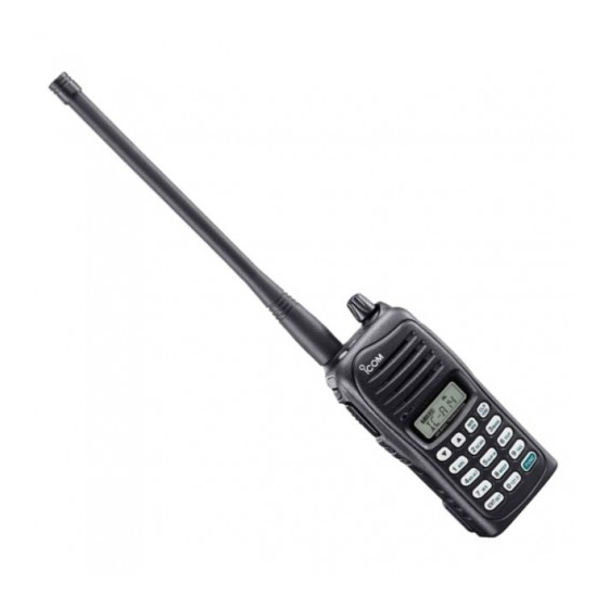
Icom IC-A14 Service Manual
Hide thumbs
Also See for IC-A14:
- Instruction manual (48 pages) ,
- Service manual (7 pages) ,
- Information (6 pages)
Table of Contents
Advertisement
Advertisement
Table of Contents

Related Manuals for Icom IC-A14


Summary of Contents for Icom IC-A14
- Page 1 VHF AIR BAND TRANSCEIVER S-14417XZ-C1 Jan. 2008...
- Page 2 8. READ the instructions of test equipment throughly before connecting a test equipment to the transceiver. Icom, Icom Inc. and logo are registered trademarks of Icom Incorporated (Japan) in the United States, the United Kingdom, Germany, France, Spain, Russia and/or other countries.
-
Page 3: Table Of Contents
CONTENTS SECTION SPECIFICATIONS SECTION INSIDE VIEWS SECTION DISASSEMBLY INSTRUCTION SECTION CIRCUIT DESCRIPITON RECEIVER CIRCUITS............4-1 TRANSMITTER CIRCUITS . -
Page 4: Specifications
200 (20 CH × 10 BANKS) IC-A14 IC-A14S • Power supply requirement : Specifi ed Icom’s battery packs 7.4 V DC standard • Usable temperature range : –10˚C to +60˚C (+14°F to +140°F) • Current drain (at 7.4 V DC) : 1.5 A... -
Page 5: Inside Views
SECTION 2 INSIDE VIEWS • PA UNIT (TOP VIEW) (BOTTOM VIEW) PRE-DRIVE AMP DRIVE AMP (Q4: 2SC3775) (Q3: RD01MUS1) POWER AMP (Q2: RD12MVS1) • MAIN UNIT (TOP VIEW) (BOTTOM VIEW) DISCRIMINATOR (X4: JTBM450CX24) TX and RX VCOs AF POWER AMP (IC31: TDA8547TS) 1st IF FILTER (FI3: FL-417) -
Page 6: Disassembly Instruction
SECTION 3 DISASSEMBLY INSTRUCTION w Unsolder total of 8 points from the shield cover then 1. Removing the front panel q Remove the VR knob and antenna nut. remove it. e Unscrew 2 screws from the side plate then remove it. w Unscrew 2 screws from the bottom. -
Page 7: Receiver Circuits
SECTION 4 CIRCUIT DESCRIPTION 4-1 RECEIVER CIRCUITS RF CIRCUITS The tuned-BPF is adjusted so that it responds to receiving RF circuits consist of RF fi lters, antenna switch (ANT SW), frequency and rejects all others, by the variable capacitor RF amplifi er (RF AMP), etc., and extracts and amplifi es the whose capacitance is varied by applied tuning voltages;... - Page 8 AGC (Automatic Gain Control) CIRCUITS SQUELCH CIRCUITS The squelch circuit cuts off the AF output signals when no For receiving AM signals RF signals are received. The AGC circuit effectively reduces the RX signal level if the signal is strong, and raises it when it is weaker. The •...
-
Page 9: Transmitter Circuits
4-2 TRANSMITTER CIRCUITS TX AF CIRCUITS The ALC (Automatic Level Control) AMP is an amplifier The TX AF circuit consists of microphone amplifier (MIC which controls its gain automatically according to the MIC AMP), ALC and AF fi lters. ALC (Automatic Level Control) is signals level. -
Page 10: Frequency Synthesizer Circuits
4-3 FREQUENCY SYNTHESIZER CIRCUITS PLL (Phase Locked Loop) CIRCUIT The PLL circuit provides stable oscillation for both of the A VCO is an oscillator whose oscillating frequency is TX and 1st LO frequencies (for RX). By comparing fedback determined by the applied volatge. This transceiver has two VCO output and reference frequency signals, the PLL VCOs;... -
Page 11: Port Allocations
4-4 PORT ALLOCATIONS • CPU (IC26) LINE NAME DESCRIPTION STATUS CONDITION Ext. [PTT] input. High While transmitting. (=[PTT] is pushed.) UNLK PLL unlock signal from the PLL IC (IC29). While PLL is unlocked. Clock signal to the DAC (IC17). – –... -
Page 12: Voltage Block Diagram
• CPU (IC26) (continued) LINE NAME DESCRIPTION STATUS CONDITION MMUTE MIC mute SW (Q51) control signal. While TX AF line is mute. SEG1– LCD (DS1) segments. – – SEG34 COM1– LCD (DS1) common terminal. – – COM4 • DAC (IC17) LINE NAME DESCRIPTION BPF tuning volatages. -
Page 13: Parts List
7030005120 S.RES ERJ2GEJ 102 X (1 k) 91.8/34 1790001250 S.DIO MA2S111-(TX) [IC-A14S] only 28.1/8.4 1790001250 S.DIO MA2S111-(TX) [IC-A14] only 28/11 R149 7030005050 S.RES ERJ2GEJ 103 X (10 k) 90/40.1 R150 7030005230 S.RES ERJ2GEJ 334 X (330 k) 88.7/40.7 1790001250 S.DIO... - Page 14 [MAIN UNIT] [MAIN UNIT] ORDER ORDER DESCRIPTION DESCRIPTION LOCATION LOCATION R226 7030005090 S.RES ERJ2GEJ 104 X (100 k) 53.1/9 R785 7030005220 S.RES ERJ2GEJ 223 X (22 k) 79.6/10.9 R227 7030005120 S.RES ERJ2GEJ 102 X (1 k) 51/15.9 R786 7030005530 S.RES ERJ2GEJ 100 X (10) 84.2/13.9 R228 7030005050 S.RES ERJ2GEJ 103 X (10 k)
- Page 15 [MAIN UNIT] [MAIN UNIT] ORDER ORDER DESCRIPTION DESCRIPTION LOCATION LOCATION 4030017460 S.CER ECJ0EB1E102K 89.1/13 C411 4030017460 S.CER ECJ0EB1E102K 97/37.7 4030017460 S.CER ECJ0EB1E102K 84.3/13.4 C412 4030017460 S.CER ECJ0EB1E102K 94.8/37.3 4030017460 S.CER ECJ0EB1E102K 73.5/14.6 C413 4030017460 S.CER ECJ0EB1E102K 101.6/26.1 4030016790 S.CER ECJ0EB1C103K 54.7/12.8 C414 4030017460 S.CER ECJ0EB1E102K...
- Page 16 [MAIN UNIT] [PA UNIT] ORDER ORDER DESCRIPTION DESCRIPTION LOCATION LOCATION C753 4030016930 S.CER ECJ0EB1A104K 58.1/41.7 IC27 1110006490 S.IC LMV321IDCKR 17.2/22 C754 4550006250 S.TAN TEESVA 1A 106M8R 100.1/24.7 C755 4030016930 S.CER ECJ0EB1A104K 96.5/14.2 C756 4030017680 S.CER ECJ0EC1H820J 79.7/25.7 1560001371 S.FET RD12MVS1-T112 22.6/8.3 C757 4030016790 S.CER ECJ0EB1C103K...
-
Page 17: Ant Unit
[PA UNIT] ORDER DESCRIPTION LOCATION C717 4030017460 S.CER ECJ0EB1E102K 20.3/21.9 C764 4030016930 S.CER ECJ0EB1A104K 18.8/14 C765 4030017460 S.CER ECJ0EB1E102K 11.6/15.5 C766 4030017460 S.CER ECJ0EB1E102K 19.4/19.8 C770 4030017460 S.CER ECJ0EB1E102K 5.9/14.2 C790 4030017460 S.CER ECJ0EB1E102K 5.3/14.5 C791 4030007110 S.CER C1608 CH 1H 680J-T 25.2/12.9 C792 4030017640 S.CER ECJ0EC1H150J... -
Page 18: Mechanical Parts
8610012970 KNOB N-350 (Incl. MP23) MP25 8830003040 3017 ANT NUT 3310002130 FA-B02AR MP26 8810009561 SCREW BT B0 2X6 NI-ZK3 (BT) (Optional) BP-232N [IC-A14] only MP27 8810009221 SCREW BT B0 2X8 NI-ZK3 (BT) (Optional) BC-179 [IC-A14]only MP28 8810008641 0Tap 1Flat washer B0 2X4 NI-ZC3 (BT) - Page 19 Unit: mm (inch) MP13 (C) J1 (C) MP25 (C) SP1 (C) MP35 (C) W1 (C) MP8 (C) MP24 (C) MP31 (C) MP1 (C) ANT UNIT MP17 (C) MP801 (A) MP20 (C) MP33 (C) MP12* (C) MP28 (C) 32.5 (1 1.7 ( 1.7 ( 1/16 1/16...
-
Page 20: Board Layouts
SECTION 7 BOARD LAYOUTS • MAIN UNIT H100 (TOP VIEW) SP1 (CHASSIS) [KEYLOCK] • PA UNIT • ANT UNIT • DC UNIT REFV (TOP VIEW) (TOP VIEW) (TOP VIEW) C352 RFDETV J1 (CHASSIS) C296 C713 R844 R338 C792 C790 R250 B6886 C210 7 - 1... - Page 21 • PA UNIT • DC UNIT • ANT UNIT REFV (BOTTOM VIEW) (BOTTOM VIEW) (BOTTOM VIEW) RFDETV C712 R845 C796 R322 C770 C791 MP801 R331 R332 R333 R771 R843 B6884B S-14417XH-P2 Printed in Japan © 2008 Icom Inc. 7 - 2...
- Page 22 SECTION 8 BLOCK DIAGRAM MAIN UNIT U NR9210 MA2S728 Tx;118.000 - 136.975 MHz UNR9213 ANLC AM DET 2SC4738 Rx;108.000 - 136.975 MHz CFWM450D 161.650 - 163.275 MHz CERAMIC RF AGC AM P 2SC4738 0.450MHz AM P IC1;NJM2552V ANT UNIT D1,D8 RSSI D14,D15 D13,D50...
- Page 23 SECTION 9 VOLTAGE DIAGRAM MAIN UNIT (Left side) MMUTE ALCC DETMUTE SHIFT C682 0.47 R725 ANLC C681 0.47 R719 C680 0.47 RFDETV +3.6V 100K R718 DETO THERMC SPCON 2.2M R765 R720 VOL2 R722 CPU36V NOISE R723 RFDETV R724 RSSI AGCOFF T:3.5V R:3.5V R825...
-
Page 24: Main Unit (Center)
MAIN UNIT (Center) RFDETV RFDETV +3.6V IC28 NOISE RSSI REFV REFV R810 2.2K COMMON C409 C411 0.001 R849 MMUT E 0.001 R806 CONTROL C412 0.001 VCON 0.001 C410 C752 LMV321IDCK +3.6V ALCC DETMUTE 0.01 CR-783 IC17 MA2S111 R243 SHIFT VIN8 VIN1 VOUT1 VOUT8... -
Page 25: Main Unit (Right Side)
MAIN UNIT (Right side) RFDETV RFDETV MO D CP06S CP20 REFV REFV CP19 CP22 CP06S CP06S CP21 CP18 CP06S CP23 CP17 CP20 AN T CP06S CP16 ANT UNIT PA UNIT (page 11-4) (page 11-4) CP10 CP27 CP25 BATT + CP11 DC UNIT CP28 CP26... - Page 26 ANT UNIT DC UNIT PA UNIT T:2.7V R:0.0V T:5.4V T:0.73V R:0.0V R:0.0V IC27 R768 REFV LMV321IDCK 9230B-1-04Z140-PT1 R844 R767 6.8K 6.8K 6.8K T:7.3V C712 R:7.4V MPZ2012S221A TO DC UNIT TO PA UNIT E P 1 7 B A T T + CP06S MP 1 R320...
- Page 27 Phone : +34 (93) 590 26 70 Fax : +34 (93) 589 04 46 Glenwood Centre #150-6165 : http://www.icomspain.com Highway 17 Delta, B.C., V4K 5B8, Canada E-mail : icom@icomspain.com Phone : +1 (604) 952-4266 Fax : +1 (604) 952-0090 : http://www.icomcanada.com E-mail : info@icomcanada.com Unit 9, Sea St., Herne Bay, Kent, CT6 8LD, U.K.
- Page 28 S-14417XZ-C1 1-1-32, Kamiminami, Hirano-ku, Osaka 547-0003, Japan © 2008 Icom Inc.
Need help?
Do you have a question about the IC-A14 and is the answer not in the manual?
Questions and answers