Table of Contents
Advertisement
Advertisement
Table of Contents

Related Manuals for Sailor RE2100


Summary of Contents for Sailor RE2100
- Page 1 S.P. RADIO A/S AALBORG DENMARK...
- Page 3 Please note Any responsibility or liability for loss or damage in connection with the use of this product and the accompanying documentation is disclaimed. The information in this manual is furnished for informational use only, is subject to change without notice, may contain errors or inaccuracies, and represents no commitment whatsoever.
-
Page 5: Table Of Contents
RE2100 CONTENTS GENERAL INFORMATION INTRODUCTION DESCRIPTION OF SAILOR HF SSB PROGRAMME GENERAL DESCRIPTION OF SAILOR HF SSB RE2100 TECHNICAL DATA (complies with SOLAS, ITU, CEPT, MPT, DOC, FTZ, KSR, FCC) 1-3 CONTROLS PRINCIPLE OF OPERATION INSTALLATION MOUNTING POSSIBILITIES DIMENSIONS AND DRILLING PLAN... -
Page 7: General Information
RE2100 CONTENTS GENERAL INFORMATION INTRODUCTION DESCRIPTION OF SAILOR HF SSB PROGRAMME GENERAL DESCRIPTION OF SAILOR HF SSB RE2100 TECHNICAL DATA (complies with SOLAS, ITU, CEPT, MPT, DOC, FTZ, KSR, FCC) 1-3 CONTROLS PRINCIPLE OF OPERATION... - Page 9 1. Select frequency. 2. Make your call when the tune lamp has been extinguished. It has been constructed so that it fits in with the other units in the SAILOR Compact Programme 2000. 1.2 DESCRIPTION OF SAILOR HF SSB PROGRAMME The SAILOR HF SSB programme is designed to meet all requirements within HF radio communication.
-
Page 10: General Description Of Sailor Hf Ssb Re2100
1 GENERAL INFORMATION RE2100 TX control unit, consisting of output filter, power supply, and audio amplifier for RE2100 and the TX-processor. Power amplifier unit, consisting of a 600W power amplifier. Combiner unit, consisting of power splitter and power combiner. 24V DC power unit, consisting of a 24V DC to 28V and 42V DC switch mode power supply, which supplies the power amplifier unit. -
Page 11: Technical Data
67 dB below PEP with aerial coupler AT2110 Carrier Suppression: better than 46 dB below PEP Audio Response: 350 Hz to 2700 Hz at -6 dB RECEIVER RE2100 Receive System: Double conversion super heterodyne 1st IF 70 MHz. 2nd 10.73 MHz Selectivity:... - Page 12 1 GENERAL INFORMATION RE2100 Spurious and IF Rejection: better than -70 dB Cross Modulaton: better than 90 dB/uV (CEPT method of test) Desensitization: better than 100 dB/uV (CEPT method of test) AGC: less than 2 dB audio level change from 10 dB/uV to 80 dB/uV.
-
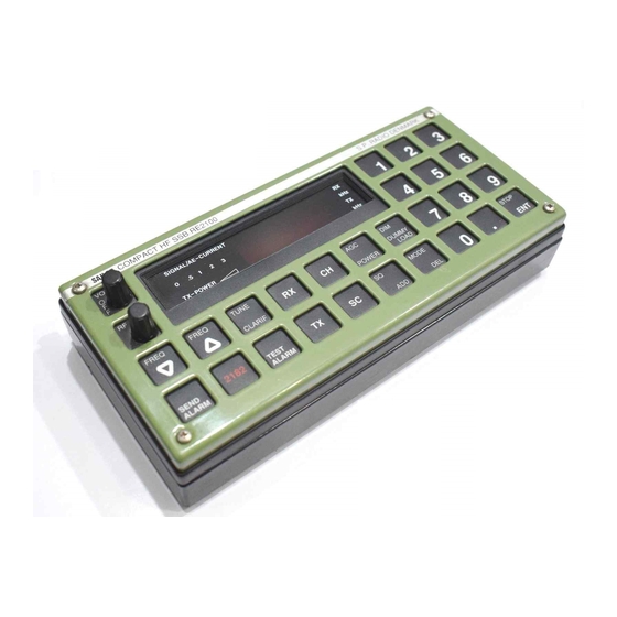
Page 13: Controls
1 GENERAL INFORMATION RE2100 1.5 CONTROLS SIGNAL AE CURRENT POWER FREQ FREQ TUNE DUMMY CLARIF POWER LOAD MODE STOP 2182 SEND TEST ALARM ALARM 29045 Volume control and on/off switch for the mains. Manual RF gain control. FREQ Tunes the receive frequency down. - Page 14 1 GENERAL INFORMATION RE2100 SEND ALARM Transmits the distress signal when pressed together with TEST ALARM. 2182 Selects the distress frequency 2182 kHz. TEST ALARM Acoustic check of the alarm signal generator. Reduces/increases the display light and switches on/off the display and keyboard panel...
-
Page 15: Principle Of Operation
The unit holds all memory, and all user defined memory is in an EEPROM, so even when supply voltage is removed, the contents of the memory is preserved. If the supply voltage to the RE2100 gets too low, the display will show error 20, and the performance of the RE2100 will be reduced. - Page 16 The input voltages from T2130 is ±18V and 9V. These voltages passes through seven series regulators to produce the necessary supply voltages to RE2100. A special ±15V for the exciter is controlled from the microprocessor, so when the transmitter has not been used for two minutes, it is switched off to reduce the power consumption in standby.
- Page 17 1 GENERAL INFORMATION RE2100 BLOCK DIAGRAM RE2100 RF in/out to T2130 SP-bus RECEIVER FRONT END RECEIVER (MODULE 1) 0.385MHz Threshold (MODULE 2) Limeting Frequency to voltage Lowpass LSB-Filter converter Filter 10.73MHz Squelch reset SCI-Rx SCI-Tx 0.385-1.6MHz SSB/AM Demodulator 2.nd +5V power...
-
Page 19: Installation
RE2100 CONTENTS INSTALLATION MOUNTING POSSIBILITIES DIMENSIONS AND DRILLING PLAN ELECTRICAL CONNECTION AND ASSEMBLING... -
Page 21: Installation 2.1 Mounting Possibilities
RE2100 INSTALLATION 2.1 MOUNTING POSSIBILITIES TABLETOP AND DECKHEAD Mounting bracket H2055 which offers the same possibilities for the loudspeakers H2054 and H2074. Mounting kit H2068 and H2055 PAGE 2-1... - Page 22 Mounting kit H2063 which offers the same possibilities for the loudspeakers H2054 and H2074. Mounting kit H2062 or Mounting kit H2064. IN CONJUNCTION WITH OTHER SAILOR EQUIPMENT Look up the INSTALLATION section for the SAILOR unit in question PAGE 2-2...
- Page 23 Permits a wide variety of installation possibilities, such as tabletop, bulkhead or deckhead. For other possibilities such as console installation, the SAILOR 19" rack or all units in the Compact programme assembled on the bulkhead, see special information concerning installation of the Compact programme.
- Page 24 2 INSTALLATION RE2100 MOUNTING KIT H2068 AND H2055 WEIGHT Lashing kit H2068: 1.5 kg Mounting kit H2055: 1.5 kg Loudspeaker H2054: 5.5 kg PAGE 2-4 Loudspeaker H2074: 4.0 kg HF SSB RE2100: 4.5 kg...
- Page 25 RE2100 MOUNTING KIT H2063 Free distance must be kept to allow free air circulation ambient tempera- ture max. 40°C. WEIGHT Mounting kit H2063: 1.0 kg Loudspeaker H2054: 5.5 kg Loudspeaker H2074: 4.0 kg HF SSB RE2100: 4.5 kg PAGE 2-5...
- Page 26 RE2100 MOUNTING KIT H2064 Free distance must be kept to allow free air circulation ambient tempera- ture max. 4o°C. WEIGHT Mounting kit H2064: 1.5 kg Loudspeaker H2054: 5.5 kg Loudspeaker H2074: 4.0 kg HF SSB RE2100: 4.5 kg PAGE 2-6...
- Page 27 RE2100 MOUNTING KIT H2062 Free distance must be kept to allow free air circulation ambient tempera- ture max. 40 WEIGHT Mounting kit H2062: 1.5 kg Loudspeaker H2054: 5.5 kg Loudspeaker H2074: 4.0 kg HF SSB RE2100: 4.5 kg PAGE 2-7...
- Page 28 RE2100 2.3 ELECTRICAL CONNECTION AND ASSEMBLING HF SSB RE2100 is the control unit in SAILOR compact HF SSB programme 2000. RE2100 can therefor be the control unit in a 250W transmitter system or a 600/1200W system. For information how to...
-
Page 29: Service
RE2100 CONTENTS SERVICE MAINTENANCE ALIGNMENT INSTRUCTIONS PROPOSAL FOR NECESSARY TEST EQUIPMENT TROUBLE SHOOTING PERFORMANCE CHECK 3.5.1 PERFORMANCE CHECK OF DISPLAY AND KEYBOARD 3.5.2 PERFORMANCE CHECK OF RECEIVER 3-11 3.5.3 PERFORMANCE CHECK OF EXCITER 3-18 MODULE PERFORMANCE CHECK 3-21 3.6.1 MODULE PERFORMANCE CHECK OF RECEIVER UNIT 3-22 3.6.2... -
Page 31: Service 3.1 Maintenance
3.1 MAINTENANCE PREVENTIVE MAINTENANCE If the HF SSB RE2100 has been installed in a proper way the maintenance can, dependent on the environments and working hours, be reduced to a performance check at the service workshop at intervals, not exceeding 12 months. A complete performance check list is enclosed in this manual, chapter 3.5 PERFORMANCE CHECK. - Page 32 3 SERVICE RE2100 3.3 PROPOSAL FOR NECESSARY TEST EQUIPMENT OSCILLOSCOPE: Bandwidth DC-35 MHz Sensitivity 2mV/div Output Impedance 1 Mohm//20 pF E.g. Philips type PM3050 PASSIVE PROBE: Attenuator 20 dB Input Impedance 10 Mohm//15 pF Compensation Range 10-30 pF E.g. Philips type...
- Page 33 3 SERVICE RE2100 TEST PROBE ceramic AA119 AA119 To multimeter ceramic LAYOUT OF THE PROBE 10.00 12.00 70.00 Metal tube Insulating material 25079 50 OHM DUMMY LOAD 50 ohm -> 50 ohm: EMF-loss 20 dB PAGE 3-3...
- Page 34 3010 TESTBOX To test all the functions of the RE2100 is very difficult when no transmitter T2130 is available. For that reason S. P. Radio has developed and produced a testbox. When using this testbox it is possible in an easy way to test all the inputs and outputs of the RE2100.
- Page 35 3 SERVICE RE2100 DIAGRAM TESTBOX PAGE 3-5...
- Page 36 If no testbox is available, it is possible to operate the RE2100 by connecting the power supply directly to the 25-pin connector, which is located at the back of the RE2100. In this 25 pin connector it is possible to find all the other inputs, outputs, and testpoints. The pin configuration for this connector is listed in chapter 2.3 ELECTRICAL CONNECTION AND ASSEMBLING.
- Page 37 If the fault is not found there, check if an error message has been shown in the RX display of the RE2100. The error codes listed below are error messages, which are generated by the RE2100, and they therefore indicate a fault in this unit.
- Page 38 See instruction manual for T2130, chapter 3.4. If the error codes indicate that the fault may be found in the RE2100, the fault is probably no transmitter signal from the RE2100. The exciter can then, without any damage to the transmitter, be set on by activating the test programme SP-05-0.
-
Page 39: Performance Check Of Display And Keyboard
3.3 PROPOSAL FOR NECESSARY TEST EQUIPMENT. If no testbox is available, it is possible to operate the RE2100 by connecting the power supply directly to the 25 pin connector, which is located at the back of the RE2100. The pin configuration for this connector is listed in chapter 2.3 ELECTRICAL CONNECTION AND ASSEMBLING. - Page 40 3 SERVICE RE2100 Press the keyboard ENT key. Select test programme SP-00-3. Control that the two led’s marked SP-BUS-TEST on the testbox are alight. Press the keyboard TUNE button. Turn the RF GAIN button fully counter clockwise. Control that the bars in the signal meter are all alight.
-
Page 41: Performance Check Of Receiver
3.5.2 PERFORMANCE CHECK OF RECEIVER Connect the RE2100 with the testbox for RE2100 and connect the power supply and a loudspeaker to the proper inputs on the testbox. The necessary test equipment to carry out a performance check is described in this manual, chapter 3.3 PROPOSAL FOR NECESSARY TEST EQUIPMENT. - Page 42 3 SERVICE RE2100 Measurement of the signal to noise SND/N. With the specified test signal applied to the receiver, the measurement of SND/N is performed as described below. SSB MODE Turn the RF-GAIN control fully clockwise and make sure that the AGC is operative.
- Page 43 3 SERVICE RE2100 Measure the signal distortion SND/ND with the distortion meter. The measured distortion SND/ND shall be better than the figures given in the table in point 5. 3.5.2.3 PERFORMANCE CHECK OF RECEIVER AUDIO PASSBAND Connect the signal generator to the aerial socket through a 50 ohm dummy load.
- Page 44 3 SERVICE RE2100 3.5.2.4 PERFORMANCE CHECK OF RECEIVER CLARIFIER AND FREQUENCY Connect the signal generator to the aerial socket through a 50 ohm dummy load. Choose receiver frequency f , signal generator frequency f , and the generator output level V according to point 6.
- Page 45 The increase in AF output level measured with the voltmeter shall be less than 2 dB. Connect 0 dBm output from the testbox to channel A on the oscilloscope. Connect the SP-BUS output socket on RE2100 to channel B on the oscilloscope. Select test programme SP-04-6.
- Page 46 3 SERVICE RE2100 SSB ATTACK A = 0.5V/div 20 msecs/div B = 5V /div. Set the timebase on the oscilloscope to 200 msecs/div. Control that the oscilloscope displays the response shown in figure SSB decay. SSB DECAY A = 0.5V/div.
- Page 47 Control that the squelch closes after about 10 secs. 3.5.2.7 PERFORMANCE CHECK OF RECEIVER EXTERNAL CONNECTIONS If no testbox for RE2100 is available, the connections can be found and checked in the 25 pin connector and the 9 pin connector at the back of the RE2100.
-
Page 48: Performance Check Of Exciter
No tone or noise shall now be heard from the loudspeaker and approx. 2 bars in the signal strength meter are alight. Release the RX mute switch. Activate the TEST ALARM button on RE2100 and control that the alarm tones can be heard in the handset earpiece 3.5.3 PERFORMANCE CHECK OF EXCITER Connect the RE2100 with the testbox for RE2100. - Page 49 Adjust the oscilloscope gain until full deflection (8 div.) is seen on the screen. Toggle the MODE switch on RE2100 between J3E, R3E, H3E, and TELEX, and control that the deflection is approx. the same in all the classes of emission 8.0 +/-1.0 div.
- Page 50 Connect the LF signal generator to the AF TO TX input on the testbox. Adjust the LF signal generator output to 3Vpp/1600 Hz. Select the emission mode TELEX on RE2100. Set the testbox switch MIC.KEY on. Control that the HF output shown on the oscilloscope is 4.0 +/-0.5Vpp.
- Page 51 The module performance check is carried out with all modules mounted in the HF SSB RE2100, and if a testbox is available, it should be used. The RE2100, the power supply, and the handset are all connected to the testbox as described in chapter 3.3. PROPOSAL FOR NECESSARY TEST EQUIPMENT.
-
Page 52: Module Performance Check Of Receiver Unit
Impedance matching between generator and receiver module. Connect the generator to receiver module through the impedance matching network shown above. Connect the voltmeter to earpiece output at testpoint TR2-1 for measuring the AC-voltage. Turn the RE2100 on. Choose generator frequency f and generator output level V as specified in point 6. - Page 53 The frequency of the carrier reinjection signal is 10.73152 MHz and is given by the TCXO. Turn the RE2100 on and select J3E-USB mode. To check the LO2 signal, connect the diode probe across the resistor R188-1, which is located at the output of the LO buffer at the Receiver Unit (module 1).
- Page 54 Connect the voltmeter to testpoint TP1-1 for measuring the DC voltage at the level detector output. Connect the counter to earpiece output at testpoint TP2-1. Turn the RE2100 on. Turn the RF gain control fully clockwise and make sure that the AGC is operative.
- Page 55 3 SERVICE RE2100 AM MODE Repeat points 1, 2 and 4-6. Make sure that H3E mode (AM) is selected. Repeat point 8-11. Increase generator output level V by 6 dB. To check the 6 dB bandwidth, key-in the frequencies 986,7 kHz and 993.3 kHz, and control in each case the voltage at testpoint TP1-1 to be above 5 volt.
- Page 56 3 SERVICE RE2100 Below the threshold level the input signal is too weak to be detected by the AGC circuit. The gain of the 2nd IF amplifier is then unregulated and the receiver output level will increase as 1:1 with increasing input level.
- Page 57 Connect the generator to the aerial socket at the front end unit (module 2). Connect the voltmeter to testpoint TP2-1 for measuring the AC voltage at the earpiece output. Turn the RE2100 on and turn the RF gain control fully clockwise. Choose generator frequency f...
- Page 58 Select external trig source, DC trig mode, and positive slope trig. Turn the RE2100 on and turn the RF gain control fully clockwise. Choose generator frequency and generator output level V as specified in point 12.
- Page 59 Connect the generator to the aerial socket at the front end unit (module 2). Connect the voltmeter and a distortion meter to detector output at U06, pin 6. Turn the RE2100 on, and turn the RF gain control fully clockwise. Choose generator frequency f...
- Page 60 Connect the generator to the aerial socket at the front end unit (module 2). Connect the voltmeter and the counter to testpoint TP2-1 (earpiece output). Turn the RE2100 on and turn the RF gain control fully clockwise. Choose generator frequency f...
- Page 61 1.5%. 3.6.1.9 CHECK OF SQUELCH CIRCUIT The squelch circuit in the RE2100 is voice activated and it works in principle by detecting deviations in the frequency of the received signal. This relative complex squelch function is implemented by means of four separate blocks, which are: 1.
-
Page 62: Module Performance Check Of Front End Unit
3.6.2 MODULE PERFORMANCE CHECK OF FRONT END UNIT This chapter contains the following sections: 3.6.2.1. Check of Sensitivity (RE2100) 3.6.2.2. Check of Front End Gain 3.6.2.3. Check of Mute and RX/TX Switch 3.6.2.4. Check of Selection Circuit for Pre-Filters 3.6.2.5. - Page 63 3 SERVICE RE2100 3.6.2.1 CHECK OF SENSITIVITY(RE2100) The sensitivity of the entire receiver can in J3E mode be calculated from the following equation: SENS 10 log (F - 1 ) - 7 dB (dB/uV) front front where the following figures shall be taken as typical values: = 5.2...
- Page 64 3 SERVICE RE2100 t l i f NOTE! The signal levels given in point 6 are referring to the output of the 50 ohm impedance matching network, which has an EMF insertion loss of 20 dB. To obtain the setting of the signal generator, the insertion loss of 20 dB must be added to the levels given in point 6.
- Page 65 The resistor R185-1 must be disconnected as shown above, before the termination of the Front End Unit can be implemented. Terminate the Front End Unit as shown in the figures above. Turn the RE2100 on. Choose generator frequency f , generator output level V...
- Page 66 The mute relay RE01-2 is used for external mute functions and for protection of the Front End Unit, when the RE2100 is switched off. The mute function is checked by toggling the relay RE01, which is done by means of the service programme SP-04-6.
-
Page 67: Module Performance Check Of Synthesizer Unit
+ 70,000,640 MHz where f is the receiver frequency. Connect the voltmeter through the diode probe across the coil L41-2. Turn the RE2100 on. Key-in the receiver frequency 2182 kHz. Control the measured DC voltage to be 7.5V +/-1V 3.6.3... - Page 68 Turn the RE2100 on. NOTE! The RE2100 must be on for at least 15 minutes before the check is carried out. Connect the counter to TP4-3 through passive probe. Check the frequency on TP4-3 to be 10.731520 MHz +/-1 Hz.
- Page 69 3.6.3.3 CHECK OF PLL2 The PLL2 consists of two independent VCO’s and is capable of delivering two different signals with the frequencies 59.26912 MHz and 80.73216 MHz. Turn the RE2100 on. Connect the voltmeter to TP5-3. Connect the counter to TP7-3.
-
Page 70: Module Performance Check Of Exciter Unit
Connect a tone generator (1000 Hz) to the testbox at the BNC-socket “AF to TX”. If a testbox is not available, connect the tone generator directly to the handset plug on the RE2100 (to J03-2, pin 4). Connect it with a capacitor 22 uF/25V because of the DC voltage on the microphone terminal Connect a scope probe to Q04-4 emitter (TP1-4). - Page 71 Connect a tone generator to the testbox at the BNC-socket “AF to TX”. If a testbox is not available, connect the tone generator directly to the handset plug on the RE2100 (to J03-2, pin 4). Connect it with a capacitor 22 uF/25V because of the DC voltage on the microphone terminal. Set the tone generator output level to 0.3 Vpp.
-
Page 72: Performance Check Of Microprocessor Module
3 SERVICE RE2100 3.6.4.6 CHECK OF STEP ATTENUATOR Select service programme SP-05-0 and press handset key. Connect a scope probe to R169-4 (TP5-4) and read the signal to 0.55Vpp +/-0.05V. In order to check the liniarity of the step attenuator, please see section 3.7.3.6. points 6-9. - Page 73 3 SERVICE RE2100 CHECK OF MICROPROCESSOR Control of Strap in P02. If the strap is connected between pin 1 and pin 2, the microprocessor will read the programme from internal ROM. This is only used if the microprocessor U07 is mask programmed. In that case the ROM U06 will not be mounted.
- Page 74 3 SERVICE RE2100 Control of Tune Tone Connect an oscilloscope to emitter of Q01 and press the digits 0-2-0 and ENT. The display will show “SP-02-0”. Control that the wave form seen is approx. equal to the one shown below. Press STOP to stop the tone.
- Page 75 3 SERVICE RE2100 Check of SPI Data Connect an oscilloscope channel A to U10 pin 4 and channel B to U10 pin 10. Set TB=50 uS. Control that the two wave forms are the same. The voltage is 5Vpp +/-0.5V.
- Page 76 3 SERVICE RE2100 Connect an oscilloscope channel A to U09 pin 13. Set TB=500uS and control the wave form as shown below. Control the same wave form on U09 pin 14 and 15. CHECK OF SP-BUS TRANSMITTER/RECEIVER Press the digits 0 and 1 at the same time. The equipment will now be in Quick Service mode and the display will show “SP- “.
-
Page 77: Module Performance Check Of Power Unit
Tune the signal generator to 22 MHz and read on the scope the voltage to 3.5 Vpp +/- 0.5V 3.7 ADJUSTMENT PROCEDURE This chapter contains the adjustment procedure for all adjustable components in the RE2100. 3.7.1 ADJUSTMENT PROCEDURE FOR FRONT END AND RECEIVER UNIT This chapter contains the following sections: 3.7.1.1. - Page 78 Connect a voltmeter to test point TP1-1 for measuring the DC-output voltage from the AGC level detector. Turn the RE2100 on. Select service programme SP-04-0 as described in section 3.10.1. of this manual. Tune the transformer TR01-1 (Receiver Module) and the trimming coil L37-2 (Front End Module) to maximum meter deflection.
- Page 79 The signal meter is adjusted by trimming the resistor R76-1, which is located at the receiver unit (module1). Disconnect any input to the aerial socket. Turn the RE2100 on and make sure that J3E-mode (SSB) is selected and that the AGC is operative. Adjust R76-1 until the first LED-bar in the display is just about to light.
-
Page 80: Adjustment Procedure For Synthesizer Unit
TP4-3 (collector of transistor Q26-3). Turn the RE2100 on NOTE! The RE2100 must be on for at least 15 minutes before the adjustment is carried out. Connect the counter to TP4-3 through passive probe. Adjust the TCXO, until the frequency at TP4-3 is 10.731520 MHz +/-1 Hz. - Page 81 VCO bands and the coils are adjusted until the output voltage from the active loop filter is -11.0 Volt. Turn the RE2100 on. Connect the voltmeter to TP1-3. Key-in the RX-frequencies and adjust VCO coils according to table 4 until voltage on TP1-3 is -11.0 Volt.
-
Page 82: Adjustment Procedure For Exciter Unit
3 SERVICE RE2100 3.7.3 ADJUSTMENT PROCEDURE FOR EXCITER UNIT This chapter contains the following sections: 3.7.3.1. Adjustment of Compressor and AF Limiter 3.7.3.2. Adjustment of Carrier Limit Amplifier 3.7.3.3. Adjustment of Modulator 3.7.3.4. Adjustment of RF Limiter 3.7.3.5. Adjustment of Carrier Insertion 3.7.3.6. - Page 83 3 SERVICE RE2100 3.7.3.3 ADJUSTMENT OF MODULATOR Connect scope probe to the connection between C66-4 and C67-4 (TP3-4). Select service programme SP-05-0. Press handset key. Adjust TR01-4 to maximum signal. Release handset key. Select service programme SP-05-1. Select H3E on the keyboard.
- Page 84 3 SERVICE RE2100 Adjust R92-4 until the deflection on the screen of the carrier signal is 4.4 div. Release handset key. 3.7.3.6 ADJUSTMENT OF STEP ATTENUATOR Connect scope probe to emitter of Q18-4 (TP5-4). Select service programme SP-05-0. Press handset key.
-
Page 85: Adjustment Procedure For Power Unit
3 SERVICE RE2100 3.7.3.7 ADJUSTMENT OF 70 MHz IF When using the two service programmes SP-05-1 and SP-05-3, the 70 MHz IF filter can be adjusted. Connect scope probe to the output of the Power Unit at PO4-8 (TP1-8). Select service programme SP-05-3. - Page 86 3.8 NECESSARY ADJUSTMENT AND CHECK AFTER REPAIR GENERAL After repair of the RE2100 it may be necessary to do some adjustments and checks. The extent of these adjustments and checks can only be decided by the person, who has done the repair, and this manual section must only be looked upon as a guide.
- Page 87 3 SERVICE RE2100 Repair in LO1 Buffer Execeute 3.5.2.1. Performance Check of Receiver Sensitivity. SYNTHESIZER UNIT (MODULE 3) After a Change of the Module Execute 3.5.2.1. Performance Check of Receiver Sensitivity, and 3.5.2.4. Performance Check of Receiver Clarifier and Frequency.
- Page 88 Any repair of the RE2100 must be followed by a performance check, and after reinstallation a function check must be carried out in order to make sure that the fault has been repaired and that the RE2100 is working correctly together with the installed transmitter T2130 and aerial coupler AT2110.
- Page 89 3 SERVICE RE2100 Toggle the keyboard button MODE, until J3E mode is chosen. Notice that no beat note is heard in the loudspeaker. Press the keyboard FREQ arrow buttons to toggle the 100 Hz decimal up and down. Control that the beat note heard in the loudspeaker changes with the 100 Hz steps.
-
Page 90: Selection And Description Of The Service Programmes
3.10 SELECTION AND DESCRIPTION OF THE SERVICE PROGRAMMES 3.10.1 HOW TO SELECT A SERVICE PROGRAMME In order to help the operator, and the service engineer during installation or repair, the RE2100 has some built-in service programmes. The RE2100 has a service mode, which is activated by pressing the keyboard buttons 1 and 0 simultaneously. - Page 91 SP-05-X TEST OF EXCITER AND POWER MODULE When the RE2100 is not connected with a transmitter T2130, it is not possible to activate the exciter module. It is therefore necessary to activate a test programme to get the exciter to work.
- Page 92 3 SERVICE RE2100 SP-05-1 EXCITER ACTIVATED IN TELEPHONY MODE The exciter output frequency is set to fTX = 22000.0 kHz, LF signal generator can be connected to testbox terminal AF to Telex, and the handset key is valid. Mode shift is possible, but the modulation is turned off in H3E mode.
-
Page 93: Mechanical Disassembling And Module Location
RE2100 CONTENTS MECHANICAL DISASSEMBLING AND MODULE LOCATION ADJUSTMENTS AND LOCATIONS... - Page 95 RF Gain On / Off / Vol Display Rear Chassis Rear Chassis Cabinet Frontplate Remove To disassemble RE2100 Cable to Processor Unit Main Cable Heat Zink for Power Unit (Module 8) Remove To disassemble Front plate Remove To disassemble Heat Zink...
- Page 96 4 MECHANICAL DISASSEMBLING AND MODULE LOCATION RE2100 Keyboard Foil Light Conductor Front Chassis Keyboard Unit (Module 5) Synthesizer Unit (Module 3) Swing Chassis Exciter Unit (Module 4) Right Side Chassis Left Side Chassis Display (Module 7) To disassemble Front Chassis...
- Page 97 4 MECHANICAL DISASSEMBLING AND MODULE LOCATION RE2100 Synthesizer Unit (Module 3) Exciter Unit (Module 4) Receiver Unit (Module 1) RF Shields RF Shields Front End (Module 2) Processor Unit (Module 5) PAGE 4-3...
-
Page 99: Circuit Description And Schematic Diagrams
RE2100 CONTENTS CIRCUIT DESCRIPTION AND SCHEMATIC DIAGRAMS RECEIVER UNIT (MODULE 1) PART NO. 625631 FRONT END UNIT (MODULE 2) PART NO. 625632 SYNTHESIZER UNIT (MODULE 3) PART NO. 625633 5-13 EXCITER UNIT (MODULE 4) PART NO. 625634 5-23 PROCESSOR UNIT (MODULE 5) PART NO. 625635 5-29 KEYBOARD UNIT (MODULE 6) PART NO. -
Page 101: Receiver Unit (Module 1) Part No. 625631
RE2100 CIRCUIT DESCRIPTION AND SCHEMATIC DIAGRAMS 5.1 RECEIVER UNIT (MODULE 1) PART NO. 625631 The receiver unit consists of a 70.0 MHz to 10.7 MHz mixer followed by an SSB/AM filter and a gain regulated IF amplifier. From the amplifier the signal is fed to the detector and low frequency filter unit. The receiver unit contains low frequency derived squelchs which can be set to control the low frequency output. - Page 102 5 CIRCUIT DESCRIPTION AND SCHEMATIC DIAGRAMS RE2100 DETECTOR The detector circuit, which can demodulate A3E, H3E, R3E, and J3E is built- up around U05. Switching between the two different detector modes, AM and SSB mode is controlled by the microprocessor through U10, Q17 and the diode switching circuit built-up around D17-D20. AM: D18 and D20 ON, SSB: D17 and D19 ON.
- Page 103 IC’s U7, U8, and U9. These switches are used to control the transfer of AF signals between the RE2100 and the peripheral equipment, which as an example could be a telex modem, a duplex receiver, and one or more remote control units. The interconnection between the individual switches is shown in the block diagram below.
- Page 104 The constant voltage divider is used in the situation where an intercom call to the RE2100 is detected. This situation is indicated by a ringing tone in the loudspeaker and to avoid this tone from vanishing it must necessarily be kept independent of the volume potentiometer.
- Page 105 5 CIRCUIT DESCRIPTION AND SCHEMATIC DIAGRAMS RE2100 MICROPROCESSOR CONTROLLING The output from the comparator U01/1 is led to the microprocessor. If the microprocessor detects a high voltage, it will turn the squelch switch ON and the AF-signal will then reach the loudspeaker, the earpiece and the 0 dBm amplifier.
- Page 106 5 CIRCUIT DESCRIPTION AND SCHEMATIC DIAGRAMS RE2100 COMPONENT LOCATION RECEIVER UNIT MODULE 1 View from component side with upper side tracks. View from component side with lower side tracks. PCB rev. 25631H PAGE 5-6 9324...
- Page 107 5 CIRCUIT DESCRIPTION AND SCHEMATIC DIAGRAMS RE2100 RECEIVER UNIT MODULE 1 TEST CONDITIONS Receiver frequency: = 2058.24kHz Receiver mode: J3E/USB Generator frequency: = 2059.24kHz 10mV/DIV with 10:1 probe Generator level: 0.05uSec/DIV = 117dB/µV Þ P = 4dBm Generator mode: The generator signal must be feed to the aerial socket at the Front End Unit.
- Page 108 5 CIRCUIT DESCRIPTION AND SCHEMATIC DIAGRAMS RE2100 PAGE 5-8...
-
Page 109: Front End Unit (Module 2) Part No. 625632
5 CIRCUIT DESCRIPTION AND SCHEMATIC DIAGRAMS RE2100 5.2 FRONT END UNIT (MODULE 2) PART NO. 625632 This module consists of a transmit/receive relay and the receiver front end. The front end consists of a receiver input protection circuit, a radio frequency filter unit, a radio frequency to first intermediate frequency (70 MHz) mixer, and a first IF (70 MHz) filter unit. - Page 110 5 CIRCUIT DESCRIPTION AND SCHEMATIC DIAGRAMS RE2100 COMPONENT LOCATION FRONT END MODULE 2 View from component side with upper side tracks. View from component side with lower side tracks. PCB rev. 25632H PAGE 5-10 9344...
- Page 111 5 CIRCUIT DESCRIPTION AND SCHEMATIC DIAGRAMS RE2100 FRONT END MODULE 2 TEST CONDITIONS Receiver frequency: = 2058.24kHz Receiver mode: J3E/USB Generator frequency: = 2059.24kHz Generator level: = 117dB/µV ⇒ P = 4dBm Generator mode: The generator signal must be feed to the aerial socket at the Front End Unit.
- Page 112 5 CIRCUIT DESCRIPTION AND SCHEMATIC DIAGRAMS RE2100 PAGE 5-12...
-
Page 113: Synthesizer Unit (Module 3) Part No. 625633
5 CIRCUIT DESCRIPTION AND SCHEMATIC DIAGRAMS RE2100 SYNTHESIZER UNIT (MODULE 3) PART NO. 625633 The synthesizer unit consists of two phase locked loops. Phase locked loop 1 generates the signal used as injection to the first mixer in the front end module and as the injection to the second mixer in the exciter unit. - Page 114 5 CIRCUIT DESCRIPTION AND SCHEMATIC DIAGRAMS RE2100 PASSIVE LOOP FILTER The components R28, R31, C11, C51, C54, and L22 constitute a chebychev lowpass filter with cut-off frequency equal to approximately 10 kHz. The major task of the passive filter is to prevent spurious signals arised from the phase detector and divider circuit, to modulate the VCO and generate sidebands to the VCO output signal.
- Page 115 5 CIRCUIT DESCRIPTION AND SCHEMATIC DIAGRAMS RE2100 API CIRCUIT The circuit delivers signal to the modulus control logic and correction signal (API voltage) for the phase detector. The circuit is built-up around a 12-bit digital accumulator constituted by U2, U3, U4, U7, U8, U9, and U12 containing a fraction register, a binary adder, and a sum latch.
- Page 116 5 CIRCUIT DESCRIPTION AND SCHEMATIC DIAGRAMS RE2100 PHASE LOCKED LOOP 2 The change between transmitted and received upper and lower sideband is generated by a frequency change in PLL2 as illustrated below. USB Receiver IF1 - Filter LSB - Filter...
- Page 117 5 CIRCUIT DESCRIPTION AND SCHEMATIC DIAGRAMS RE2100 BLOCK DIAGRAM OF USB/LSB SYNTHESIZER VCO1 LO2 to > > TCXO F(S ) 1 F(S ) 2 VCO2 LO1 to < Divider MC145158 DATA 2 Modulus CLOCK Prescaler STROBE Modulus Control 25743A From the block diagram it can be shown that the output frequency f...
- Page 118 5 CIRCUIT DESCRIPTION AND SCHEMATIC DIAGRAMS RE2100 PRESCALER BUFFER From the oscillator buffer transistor Q36 the signal is fed through the network consisting of R159 and C180 to the grounded basis transistor Q38. The local oscillator signal is amplified here and fed through the attenuator R168/R170 and the amplifier transistor Q40.
- Page 119 5 CIRCUIT DESCRIPTION AND SCHEMATIC DIAGRAMS RE2100 SYNTHESIZER WAVEFORMS The below waveforms are identified with a signal name, which can be found in the diagram of the synthesizer module (3). TEST CONDITIONS Frequency setting = 2058.24 kHz Mode = J3E/USB...
- Page 120 5 CIRCUIT DESCRIPTION AND SCHEMATIC DIAGRAMS RE2100 COMPONENT LOCATION SYNTHESIZER UNIT MODULE 3 View from component side with upper side tracks. View from component side with lower side tracks. PCB rev. 25633F PAGE 5-20 9826...
- Page 121 5 CIRCUIT DESCRIPTION AND SCHEMATIC DIAGRAMS RE2100 SYNTHESIZER UNIT MODULE 3 This diagram is valid for PCB rev. 25633F 9826 PAGE 5-21...
- Page 122 5 CIRCUIT DESCRIPTION AND SCHEMATIC DIAGRAMS RE2100 PAGE 5-22...
-
Page 123: Exciter Unit (Module 4) Part No. 625634
5 CIRCUIT DESCRIPTION AND SCHEMATIC DIAGRAMS RE2100 5.4 EXCITER UNIT (MODULE 4) PART NO. 625634 The exciter module is modulating an audio frequency into a carrier frequency. After some amplification and filtration the modulated signal is led to the power unit (module 8) for further amplification and filtration. - Page 124 5 CIRCUIT DESCRIPTION AND SCHEMATIC DIAGRAMS RE2100 MODE SELECTOR Only two bits from the shift register U07 (pin 15 and pin 1) are used to control the mode selector U08 to select the right combinations of carrier level and modulation level for the mode in question. The outputs from U08 are forward biasing or reverse biasing the switch diodes in the carrier level amplifier and in the modulation level amplifier.
- Page 125 5 CIRCUIT DESCRIPTION AND SCHEMATIC DIAGRAMS RE2100 PAGE 5-25...
- Page 126 5 CIRCUIT DESCRIPTION AND SCHEMATIC DIAGRAMS RE2100 COMPONENT LOCATION EXCITER UNIT MODULE 4 View from component side with upper side tracks. View from component side with lower side tracks. PCB rev. 25634F PAGE 5-26 9717...
- Page 127 5 CIRCUIT DESCRIPTION AND SCHEMATIC DIAGRAMS RE2100 EXCITER MODULE 4 Y=1V/DIV X=500uSec/DIV REF: GND. Y=0.1V/DIV X=500uSec/DIV REF: GND. This diagram is valid for PCB rev. 25634F 9739 PAGE 5-27...
- Page 128 5 CIRCUIT DESCRIPTION AND SCHEMATIC DIAGRAMS RE2100 PAGE 5-28...
-
Page 129: Processor Unit (Module 5) Part No. 625635
The processor module has been built up around a microprocessor of the type HD63B03VP with belonging 8.005 MHz crystal. The purpose of the microprocessor is to control the other modules in the RE2100 by means of a Serial Peripheral Interface Bus (SPI), and to scan the keyboard. Furthermore the processor must also control the Serial Communication Interface Bus (SCI), also called the SP-BUS. - Page 130 The RE2100 is the master and a number of slaves may be connected to the SP-Bus. When a slave (except from T2130) wants to be called, the slave sends an interrupt to RE2100 on the SP-Bus INTERRUPT. The transmitter and the receiver are identical in each unit connected to the SP-Bus.
- Page 131 5 CIRCUIT DESCRIPTION AND SCHEMATIC DIAGRAMS RE2100 PAGE 5-31...
- Page 132 5 CIRCUIT DESCRIPTION AND SCHEMATIC DIAGRAMS RE2100 COMPONENT LOCATION PROCESSOR UNIT MODULE 5 View from component side with upper side tracks. View from component side with lower side tracks. PCB rev. 25635M PAGE 5-32 9324...
- Page 133 5 CIRCUIT DESCRIPTION AND SCHEMATIC DIAGRAMS RE2100 PROCESSOR UNIT MODULE 5 This diagram is valid for PCB rev. 25635M 9606 PAGE 5-33...
- Page 134 5 CIRCUIT DESCRIPTION AND SCHEMATIC DIAGRAMS RE2100 PAGE 5-34...
-
Page 135: Keyboard Unit (Module 6) Part No. 625636
5 CIRCUIT DESCRIPTION AND SCHEMATIC DIAGRAMS RE2100 5.6 KEYBOARD UNIT (MODULE 6) PART NO. 625636 The keyboard consists of a 4x8 matrix of which 26 keys are used. One side is connected to the microprocessor data bus by an 8 bit driver. The other side is connected to 4 of the microprocessor ports. - Page 136 5 CIRCUIT DESCRIPTION AND SCHEMATIC DIAGRAMS RE2100 PAGE 5-36...
-
Page 137: Display Unit (Module 7) Part No. 625637
5 CIRCUIT DESCRIPTION AND SCHEMATIC DIAGRAMS RE2100 5.7 DISPLAY UNIT (MODULE 7) PART NO. 625637 The display module uses 13 pcs. 7 segments (U08-U20), 12 pcs. LED (DO3 -D14) and 1 pc. LED-bar (U01) for reading-out information to the operator. - Page 138 5 CIRCUIT DESCRIPTION AND SCHEMATIC DIAGRAMS RE2100 COMPONENT LOCATION DISPLAY MODULE 7 View from component side with upper side tracks. View from component side with lower side tracks. PCB rev. 25637D PAGE 5-38 9344...
- Page 139 5 CIRCUIT DESCRIPTION AND SCHEMATIC DIAGRAMS RE2100 DISPLAY UNIT MODULE 7 This diagram is valid for PCB rev. 25637D 9435 PAGE 5-39...
- Page 140 5 CIRCUIT DESCRIPTION AND SCHEMATIC DIAGRAMS RE2100 PAGE 5-40...
-
Page 141: Power Unit (Module 8) Part No. 625638
The power module receives three voltages +9V, +18V, and -18V from the power supply placed in the transmitter T2130. Seven regulators are converting these voltages to the different working voltages used in the RE2100. U01 and U02 deliver +15V and -15V only to the exciter module. If the transmitter has not been used for two minutes the microprocessor shuts down the regulators U01 and U02. - Page 142 5 CIRCUIT DESCRIPTION AND SCHEMATIC DIAGRAMS RE2100 COMPONENT LOCATION POWER UNIT MODULE 8 View from component side with upper side tracks. View from component side with lower side tracks. PCB rev. 25638D PAGE 5-42 9433...
- Page 143 5 CIRCUIT DESCRIPTION AND SCHEMATIC DIAGRAMS RE2100 POWER UNIT MODULE 8 Y=0.1V/DIV X=500uSec/DIV REF: GND. Y=0.1V/DIV X=500uSec/DIV REF: GND. This diagram is valid for PCB rev. 25638D 9433 PAGE 5-43...
- Page 144 5 CIRCUIT DESCRIPTION AND SCHEMATIC DIAGRAMS RE2100 PAGE 5-44...
-
Page 145: Interconnection Cable Plan
5 CIRCUIT DESCRIPTION AND SCHEMATIC DIAGRAMS RE2100 5.9 INTERCONNECTION CABLE PLAN 25918B CONNECTION CABLING 25917B 9324 PAGE 5-45... - Page 146 5 CIRCUIT DESCRIPTION AND SCHEMATIC DIAGRAMS RE2100 BLOCK DIAGRAM SUPPLY CABLING MAIN BLOCK DIAGRAM 25919B 25920A PAGE 5-46 9324...
-
Page 147: Microtelephone Installation
RE2100 CONTENTS MICROTELEPHONE INSTALLATION NORMAL INSTALLATION RE2100 AND C2140 NORMAL INSTALLATION RE2100 OR C2140 WITH 2 MICRO TELEPHONES MECHANICAL DIMENSIONS FOR HANDSET... - Page 149 RE2100 MICROTELEPHONE INSTALLATION VHF RT2047 SCRAMBLER CRY2001, RE2100, RT2047 prepared for DSC and RT2048 SHORTWAVE S130X YELLOW YELLOW WHITE BROWN BROWN BROWN TC801 TC1701 HAND KEY HAND KEY HAND KEY S801 S1701 P1701 P803 MIC PRE-AMP MIC PRE-AMP MIC PRE-AMP...
- Page 150 6 MICROTELEPHONE INSTALLATION RE2100 MICROTELEPHONE WITH ELECTRET MIC. AMP. ECI A/S 4-6-24025D/4-0-24025E 600875 POSITION DESCRIPTION MANUFACTOR TYPE PART NR. CAPACITOR ELECTROLYTIC 100uF 20% 10VDC EKI 00 BB 310 C M0E 14.607 CAPACITOR CERAMIC 10nF -20/+80% CL2 50VDC RT-HE70 SK YF 103 Z 15.170...
-
Page 151: Microtelephone Installation 6.1 Normal Installation Re2100 And C2140
Supply Terminal Block ST1, this multicable is connected to either RE2100 J3 or C2140 J1. Plug in the normal microtelephone in Hook Assembly 726233‘s J1 plug. Mount jumpers on P7 pin 1-2 and on P1 pin 1-2. Supply Terminal Block ST2 is not used. - Page 152 Supply Terminal Hook 1: this multicable is connected to either RE2100 J3 or C2140 J1. Hook 2: replace the multicable in ST1 with your own cable.Plug in the normal microtelephone in Hook Assembly 726233‘s J1 plug.
- Page 153 6 MICROTELEPHONE INSTALLATION RE2100 6.3 MECHANICAL DIMENSIONS FOR HANDSET ø4.5 ø4.5 27946 MECHANICAL DIMENSIONS FOR HANDSET HOLDER WITH MICROSWITCH ø4.5 ø4.5 26999 PAGE 6-5...
- Page 154 6 MICROTELEPHONE INSTALLATION RE2100 MECHANICAL DIMENSIONS FOR HANDSET ø4.5 ø4.5 4-0-29938 MECHANICAL DIMENSIONS FOR HANDSET HOLDER WITH MICROSWITCH ø4.5 ø4.5 4-0-29937 PAGE 6-6 9437...
-
Page 155: Parts List
RE2100 CONTENTS PARTS LIST... - Page 157 VARIOUS MANUAL RE2100 ENGLISH S.P.RADIO A/S Ver.: M2100GB VARIOUS MICROTELEPHONE WITH CRADLE RE2100/C2140 S.P.RADIO A/S 3-0-27501 727501 BASE UNIT RE2100 STD. ECI A/S 702100 POSITION DESCRIPTION MANUFACTOR TYPE PART NO. VARIOUS HOUSING FOR REAR PLATE BLACK PLASTIC 48.611 MALES SORT 162.080...
- Page 158 7 PARTS LISTS RE2100 POSITION DESCRIPTION MANUFACTOR TYPE PART NO. C20-1 CAPACITOR MKT 0.1uF 10% 63VDC PHILIPS 2222 370 75104 (78104) 11.136 C21-1 CAPACITOR CERAMIC 10nF -20/+80% CL2 50VDC RT-HE70 SK YF 103 Z 15.170 C22-1 CAPACITOR CERAMIC 1n0F 10% CL2 500VDC RT-HM60 SK YB 102 K 15.160...
- Page 159 7 PARTSLIST RE2100 POSITION DESCRIPTION MANUFACTOR TYPE PART NO. C95-1 CAPACITOR ELECTROLYTIC 22uF 20% 25VDC ELNA RJ2-25-V-220-M-T58 14.514 C96-1 CAPACITOR MKT 100nF 5% 63VDC PHILIPS 2222 370 79104 (76104) 11.135 C97-1 CAPACITOR ELECTROLYTIC 22uF 20% 25VDC ELNA RJ2-25-V-220-M-T58 14.514 C98-1...
- Page 160 7 PARTS LISTS RE2100 POSITION DESCRIPTION MANUFACTOR TYPE PART NO. D12-1 DIODE 1N4148 HIGH SPEED PHILIPS 1N4148-143 25.131 D13-1 DIODE 1N4148 HIGH SPEED PHILIPS 1N4148-143 25.131 D14-1 DIODE 1N4148 HIGH SPEED PHILIPS 1N4148-143 25.131 D15-1 DIODE 1N4148 HIGH SPEED PHILIPS 1N4148-143 25.131...
- Page 161 7 PARTSLIST RE2100 POSITION DESCRIPTION MANUFACTOR TYPE PART NO. Q13-1 TRANSISTOR AF BC548 NPN TO-92 PHILIPS BC548 (-A/-B/-C)126 28.070 Q14-1 TRANSISTOR AF BC558 PNP TO-92 PHILIPS BC558 (-A/-B/-C)-126 28.095 Q15-1 TRANSISTOR AF BC548 NPN TO-92 PHILIPS BC548 (-A/-B/-C)126 28.070 Q16-1...
- Page 162 7 PARTS LISTS RE2100 POSITION DESCRIPTION MANUFACTOR TYPE PART NO. R68-1 RESISTOR MF 12k OHM 5% 0.33W PHILIPS 2322 187 73123 02.498 R69-1 RESISTOR MF 56k OHM 5% 0.33W PHILIPS 2322 187 73563 02.514 R70-1 RESISTOR MF 100k OHM 5% 0.33W...
- Page 163 7 PARTSLIST RE2100 POSITION DESCRIPTION MANUFACTOR TYPE PART NO. R142-1 RESISTOR MF 39k OHM 5% 0.33W PHILIPS 2322 187 73393 02.510 R143-1 RESISTOR MF 1M OHM 5% 0.33W PHILIPS 2322 187 73105 02.544 R144-1 RESISTOR MF 100k OHM 5% 0.33W...
- Page 164 7 PARTS LISTS RE2100 POSITION DESCRIPTION MANUFACTOR TYPE PART NO. R216-1 RESISTOR MF 5k6 OHM 5% 0.33W PHILIPS 2322 187 73562 02.490 R217-1 RESISTOR MF 5k6 OHM 5% 0.33W PHILIPS 2322 187 73562 02.490 TR1-1 TRAFO RF 70MHz ADJUSTABLE MITSUMI L-2M7-D3/DM-7141 38.438...
- Page 165 7 PARTSLIST RE2100 POSITION DESCRIPTION MANUFACTOR TYPE PART NO. C54-2 CAPACITOR CERAMIC 120pF 2% N150 100VDC PHILIPS 2222 689 34121 15.143 C55-2 CAPACITOR CERAMIC 120pF 2% N150 100VDC PHILIPS 2222 689 34121 15.143 C56-2 CAPACITOR CERAMIC 47pF 2% N150 PHILIPS 2222 689 34479 15.102...
- Page 166 7 PARTS LISTS RE2100 POSITION DESCRIPTION MANUFACTOR TYPE PART NO. L23-2 CHOKE FIXED 1u0H 10% SIEMENS B78108-T1102-K 20.347 L24-2 CHOKE FIXED 22uH 5% SIEMENS B78108-S1223-J 20.302 L25-2 CHOKE FIXED 8u2H 10% SIEMENS B78108-T1822-K 20.358 L26-2 CHOKE FIXED 22uH 5% SIEMENS B78108-S1223-J 20.302...
- Page 167 QUAD OP.AMP. NAT/SGS LM324N 31.065 U3-2 DUAL OP AMP LM358N MOTOTOLA LM 358N 31.100 SYNTHESIZER MODULE 3 RE2100, TCXO: 0.34ppm ECI A/S 625633 w. 0.34ppm TCXO 727070 POSITION DESCRIPTION MANUFACTOR TYPE PART NO. SYNTHESIZER MODULE 3 RE2100 ECI A/S 4-6-25633E / 4-0-25633F...
- Page 168 7 PARTS LISTS RE2100 POSITION DESCRIPTION MANUFACTOR TYPE PART NO. C50-3 CAPACITOR MKT 220nF 10% 63VDC PHILIPS 2222 370 78224 11.095 C51-3 CAPACITOR MKT 47nF 5% 63VDC PHILIPS 2222 370 79473 11.156 C52-3 CAPACITOR CERAMIC 43pF 5% N150 50VDC RT-HE60-SK-PH 430 J 15.097...
- Page 169 7 PARTSLIST RE2100 POSITION DESCRIPTION MANUFACTOR TYPE PART NO. C136-3 CAPACITOR ELECTROLYTIC 47uF 20% 25VDC EKI 00 BB 247 E M0E 14.524 C137-3 CAPACITOR CERAMIC 2p7F +/-0.25pF N150 50VDC RT-HE40 SK PJ 2R7 C 15.001 C138-3 CAPACITOR MKT 22nF 5% 100VDC...
- Page 170 7 PARTS LISTS RE2100 POSITION DESCRIPTION MANUFACTOR TYPE PART NO. D5-3 DIODE SWITCH BA243, BA282 BA282 TAPED 25.386 D6-3 DIODE CAPACITANCE 4.5pF/28VDC PHILIPS BB809 26.125 D7-3 DIODE SWITCH BA243, BA282 BA282 TAPED 25.386 D8-3 DIODE CAPACITANCE 4.5pF/28VDC PHILIPS BB809 26.125...
- Page 171 7 PARTSLIST RE2100 POSITION DESCRIPTION MANUFACTOR TYPE PART NO. Q2-3 TRANSISTOR FET. BF256C PHILIPS BF256C 29.707 Q3-3 TRANSISTOR AF BC558 PNP TO-92 MOTOROLA BC558 (-A/-B/-C)ZL1 28.095 Q4-3 TRANSISTOR AF BC548 NPN TO-92 PHILIPS BC548 (-A/-B/-C)126 28.070 Q5-3 TRANSISTOR FET. BF256C...
- Page 172 7 PARTS LISTS RE2100 POSITION DESCRIPTION MANUFACTOR TYPE PART NO. R36-3 RESISTOR MF 910 OHM 5% 0.33W PHILIPS 2322 187 73911 02.471 R37-3 RESISTOR MF 5k6 OHM 5% 0.33W PHILIPS 2322 187 73562 02.490 R38-3 RESISTOR MF 36k OHM 5% 0.33W...
- Page 173 7 PARTSLIST RE2100 POSITION DESCRIPTION MANUFACTOR TYPE PART NO. R111-3 RESISTOR MF 4k7 OHM 5% 0.33W PHILIPS 2322 187 73472 02.488 R112-3 RESISTOR MF 6k8 OHM 5% 0.33W PHILIPS 2322 187 73682 02.492 R113-3 RESISTOR MF 10k OHM 5% 0.33W...
- Page 174 7 PARTS LISTS RE2100 POSITION DESCRIPTION MANUFACTOR TYPE PART NO. RE1-3 RELAY 15V DC 2A 1SH. SIEMENS V23040-A0003-B201 21.062 RE2-3 RELAY 15V DC 2A 1SH. SIEMENS V23040-A0003-B201 21.062 TR1-3 TRANSFORMER TL493 S.P.RADIO 6-0-25812 400493 TR2-3 TRANSFORMER TL493 S.P.RADIO 6-0-25812 400493...
- Page 175 7 PARTSLIST RE2100 POSITION DESCRIPTION MANUFACTOR TYPE PART NO. C20-4 CAPACITOR ELECTROLYTIC 47uF 20% 25VDC ELNA RJ2-25-V-470-M-F1 14.524 C21-4 CAPACITOR MKT 0.1uF 10% 63VDC PHILIPS 2222 370 78104 11.136 C22-4 CAPACITOR MKT 220nF 20% 63VDC MKT 1826-422/06 6-G 11.183 C23-4...
- Page 176 7 PARTS LISTS RE2100 POSITION DESCRIPTION MANUFACTOR TYPE PART NO. C95-4 CAPACITOR ELECTROLYTIC 4.7uF 20% 50VDC ELNA RJ2-50-V-4R7-M-T34 14.510 C96-4 CAPACITOR MKT 22nF 5% 100VDC PHILIPS 2222 370 89223 11.169 C97-4 CAPACITOR MKT 22nF 5% 100VDC PHILIPS 2222 370 89223 11.169...
- Page 177 7 PARTSLIST RE2100 POSITION DESCRIPTION MANUFACTOR TYPE PART NO. J3-4 SOCKET COAX 45 DEG. PCB VERSION TAIKO TMP-J01X-A2 78.517 J4-4 SOCKET COAX 45 DEG. PCB VERSION TAIKO TMP-J01X-A2 78.517 L1-4 CHOKE FIXED 82uH 5% NEOSID 00 6122 11 20.168 L2-4...
- Page 178 7 PARTS LISTS RE2100 POSITION DESCRIPTION MANUFACTOR TYPE PART NO. R38-4 RESISTOR MF 10k OHM 5% 0.33W PHILIPS 2322 187 73103 02.496 R39-4 RESISTOR MF 10k OHM 5% 0.33W PHILIPS 2322 187 73103 02.496 R40-4 RESISTOR MF 10k OHM 5% 0.33W...
- Page 179 7 PARTSLIST RE2100 POSITION DESCRIPTION MANUFACTOR TYPE PART NO. R112-4 RESISTOR MF 18k OHM 5% 0.33W PHILIPS 2322 187 73183 02.502 R113-4 RESISTOR MF 18k OHM 5% 0.33W PHILIPS 2322 187 73183 02.502 R114-4 RESISTOR MF 8k2 OHM 5% 0.33W...
- Page 180 7 PARTS LISTS RE2100 POSITION DESCRIPTION MANUFACTOR TYPE PART NO. R186-4 RESISTOR PMF 120 OHM 5% 2W PHILIPS 2322 191 31201 04.178 R187-4 RESISTOR MF 1k5 OHM 5% 0.33W PHILIPS 2322 187 73152 02.476 R188-4 RESISTOR MF 5k6 OHM 5% 0.33W...
- Page 181 7 PARTSLIST RE2100 POSITION DESCRIPTION MANUFACTOR TYPE PART NO. C39-5 CAPACITOR MKT 1uF 10% 63VDC PHILIPS 2222 370 78105 11.137 C40-5 CAPACITOR MKT 1uF 10% 63VDC PHILIPS 2222 370 78105 11.137 C41-5 CAPACITOR CERAMIC 10nF -20/+80% CL2 50VDC RT-HE70 SK YF 103 Z 15.170...
- Page 182 7 PARTS LISTS RE2100 POSITION DESCRIPTION MANUFACTOR TYPE PART NO. R48-5 RESISTOR MF 1k0 OHM 5% 0.33W PHILIPS 2322 187 73102 02.472 R49-5 RESISTOR MF 100 OHM 5% 0.33W PHILIPS 2322 187 73101 02.448 R50-5 RESISTOR ARRAY 4x100 OHM 5% 1/8W...
- Page 183 7 PARTSLIST RE2100 POSITION DESCRIPTION MANUFACTOR TYPE PART NO. S20-6 SWITCH KEYBOARD 12x12mm OMRON B3F-4005 43.601 S21-6 SWITCH KEYBOARD 12x12mm OMRON B3F-4005 43.601 S22-6 SWITCH KEYBOARD 12x12mm OMRON B3F-4005 43.601 S23-6 SWITCH KEYBOARD 12x12mm OMRON B3F-4005 43.601 S24-6 SWITCH KEYBOARD...
- Page 184 7 PARTS LISTS RE2100 POSITION DESCRIPTION MANUFACTOR TYPE PART NO. U11-7 DISPLAY LED 7 SEGMENT RED H=7mm TELEFUNKEN TDSL 1150 25.726 U12-7 DISPLAY LED 7 SEGMENT RED H=7mm TELEFUNKEN TDSL 1150 25.726 U13-7 DISPLAY LED 7 SEGMENT RED H=7mm TELEFUNKEN TDSL 1150 25.726...
- Page 185 7 PARTSLIST RE2100 POSITION DESCRIPTION MANUFACTOR TYPE PART NO. L10-8 CHOKE FIXED 1u2H 10% FASTRON MICC-1R2K-02 20.348 L11-8 CHOKE FIXED 10uH 5% NEOSID 00 6122 00 20.118 L12-8 CHOKE FIXED 10uH 5% NEOSID 00 6122 00 20.118 L13-8 CHOKE FIXED...
- Page 186 2322 187 73473 02.512 TERMINAL BLOCK 8 POLES 1.5mm2 AK500/8DS m.MESS.SKRUER 81.001 TERMINAL BLOCK 9 POLES 1.5mm2 AK500/9DS m.MESS.SKRUER 81.002 HANDSET HOLDER F. C2140 & REMOTE CONTROLLED RE2100 ECI A/S 0-0-26233 726233 POSITION DESCRIPTION MANUFACTOR TYPE PART NO. CABLE 1,5m C2140 HANDSET...
Need help?
Do you have a question about the RE2100 and is the answer not in the manual?
Questions and answers