Table of Contents
Advertisement
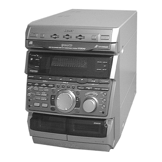
SERVICE MANUAL
HCD-VX90AV is the tuner, deck, CD and
amplifier section in MHC-VX90AV.
MICROFILM
HCD-VX90AV
Model Name Using Similar Mechanism HCD-GRX80/RXD8/RXD8S
CD
CD Mechanism Type
SECTION
Base Unit Type
Optical Pick-up Type
Model Name Using Similar Mechanism HCD-GRX80/RXD8/RXD8S
TAPE DECK
SECTION
Tape Transport Mechanism Type
SPECIFICATIONS
COMPACT DISC DECK RECEIVER
– 1 –
E Model
CDM38L-5BD34L
BU-5BD34L
KSS-213D/Q-NP
TCM-230AWR2/230PWR2
— Continued on next page —
Advertisement
Table of Contents

Related Manuals for Sony HCD-VX90AV


Summary of Contents for Sony HCD-VX90AV
- Page 1 HCD-VX90AV SERVICE MANUAL E Model HCD-VX90AV is the tuner, deck, CD and amplifier section in MHC-VX90AV. Model Name Using Similar Mechanism HCD-GRX80/RXD8/RXD8S CD Mechanism Type CDM38L-5BD34L SECTION Base Unit Type BU-5BD34L Optical Pick-up Type KSS-213D/Q-NP Model Name Using Similar Mechanism HCD-GRX80/RXD8/RXD8S...
- Page 2 WITH MARK ! ON THE SCHEMATIC DIAGRAMS AND IN THE PARTS LIST ARE CRITICAL TO SAFE OPERATION. REPLACE THESE COMPONENTS WITH SONY PARTS WHOSE PART NUMBERS APPEAR AS SHOWN IN THIS MANUAL OR IN SUPPLEMENTS PUBLISHED BY SONY. – 2 –...
-
Page 3: Table Of Contents
TABLE OF CONTENTS 1. SERVICING NOTE 8. EXPLODED VIEWS ............4 8-1. Case Section ................ 92 8-2. Chassis Section ..............93 2. GENERAL ................7 8-3. Front Panel Section ............. 94 8-4. CD Mechanism Deck Section-1 (CDM38L-5BD34L) ..95 3. DISASSEMBLY 8-5. -
Page 4: Servicing Note
SECTION 1 SERVICING NOTE HOW TO OPEN THE DISC TRAY WHEN POWER SWITCH TURNS OFF 1 Remove the Case. 2 Turn the cam to the direction of arrow. 3 Pull-out the disc tray. Note for Installation (ROTARY ENCODER) Note:When attaching the Base unit, Insert the BU cam section A into the groove of BU cam. - Page 5 MC Cold Reset • The cold reset clears all data including preset data stored in the RAM to initial conditions. Execute this mode when returning the set to the customer. Procedure: 1. Press three buttons p , ENTER/NEXT , and 1/u simultaneously. 2.
- Page 6 AMS Test Mode • This mode is used for checking the AMS operations of the tape deck. 7-819-039-12 Alignment tape, AMS-110A Procedure: 1. Press the 1/u button to turn the unit ON. 2. Set the tape (AMS-110A). 3. Press the three buttons p , ENTER/NEXT , and DISC 3 button simultaneously. 4.
-
Page 7: General
SECTION 2 GENERAL Front Panel LOCATION OF PARTS AND CONTROLS 44 PLAY MODE/DOLBY NR button 1 1/u button and indicator 22 DBFB button 23 HI-DUB button 45 EDIT DIRECTION/TUNER MEMORY 2 DEMO (STANDBY) button 24 CD SYNC button button 3 DISC 1 button and indicator 46 ECHO LEVEL knob 4 DISC 2 button and indicator 25 PHONES jack... -
Page 9: Disassembly
SECTION 3 DISASSEMBLY Note: Follow the disassembly procedure in the numerical order given. 3-1. LOADING PANEL Claws 3 Loading panel assembly 1 Turn the cam to the direction of arrow. 2 Pull-out the disc tray. 3-2. FRONT PANEL !∞ Video board !¢... -
Page 10: Cassette Lid And Tape Mechanism
3-3. CASSETTE LID AND TAPE MECHANISM 9 Tape mechanism 8 Three screws (BVTP2.6x8) 7 Two screws (BVTP2.6x8) 6 Tension spring 4 Cassette holder (L) assembly Note for installation Portion B 2 Release 3 Cassette holder (R) Portion B assembly Portion A 5 Tension spring Portion A 1 Release... -
Page 11: Disc Tray
3-5. DISC TRAY (Perform after removing the front panel.) Note:When installing the Disc tray, pull around the flat type wire to pass through the claw A and claw B , as shown in the figure. 3 Flat type wire (8 core) 4 Two claws 2 Pull-out the disc tray. -
Page 12: Test Mode
SECTION 4 TEST MODE VIDEO CD COLOR-BARS MODE On this mode, the data of the color-bars signal as a picture signal and the 1kHz sine wave signal as a sound signal are output by the mechanism control microcomputer (IC502) for video CD signal check. When measurement of the voltage and waveform on the VIDEO board, perform it in this mode. -
Page 13: Mechanical Adjustments
SECTION 5 SECTION 6 MECHANICAL ADJUSTMENTS ELECTRICAL ADJUSTMENTS Precaution DECK SECTION 0 dB=0.775V 1. Clean the following parts with a denatured alcohol-moistened swab: 1. Demagnetize the record/playback head with a head damagnetizer. record/playback heads pinch rollers 2. Do not use a magnetized screwdriver for the adjustments. erase head rubber belts 3. - Page 14 3. Mode: Playback Tape Speed Adjustment (Deck B) test tape Note: Set the test mode using the following method and begin tape P-4-A100 speed adjustment. (10kHz, –10dB) oscilloscope In the test mode, the speed will switch to double speed or normal speed each time the HI DUB button is pressed.
- Page 15 Record Bias Adjustment (Deck B) Record Level Adjustment (Deck B) Procedure: Procedure: INTRODUCTION INTRODUCTION When set to the test mode performed in Tape Speed Adjust- When set to the test mode performed in Tape Speed Adjust- ment, when the tape is rewound after recording, the “REC memory ment, when the tape is rewound after recording, the “REC memory mode”...
- Page 16 Note: Clear RF signal waveform means that the shape “◊” can be CD SECTION clearly distinguished at the center of the waveform. Note: RF signal waveform 1. CD Block is basically constructed to operate without adjustment. Therefore, check each item in order given. VOLT/DIV : 200mV 2.
- Page 17 Adjustment Location : [ BD BOARD ] — SIDE B — (RF) (VC) (TE) (FE) (AGCCON) (IOP) VIDEO SECTION Frequency adjustment frequency counter 1. Connect the frequency counter to check point of the VIDEO VIDEO board board. (27 MHz) 2. Adjust CT503 of the VIDEO board so that the frequency counter –...
-
Page 18: Diagrams
SECTION 7 DIAGRAMS 7-1. CIRCUIT BOARDS LOCATION VIDEO board CD SW board TUNER unit PANEL board TRANS board MAIN board TUNER unit is supplied as the assembled block. MOTOR (TURN) board CONNECTOR board BD board SENSOR board MOTOR (SLIDE) board 3CH AMP board LEAF SW board FRONT AMP board... -
Page 19: Block Diagrams
HCD-VX90AV 7-2. BLOCK DIAGRAMS – CD SECTION – IC421 OPTICAL PICK-UP BLOCK CD DIGITAL (KSS-213D/Q-Np) IC101 D+5V OPTICAL DIGITAL SERVO DETECTOR IC103 DIGITAL SIGNAL PRCESSOR RF AMP DIGITAL D OUT DOUT ERROR CORRECTOR PCM-D RF AC RF EQ ADATA SUMMING... -
Page 20: Video Section
HCD-VX90AV – VIDEO SECTION – D-RAM IC507 IC506 2 - 10 31 - 39 25 4 28 29 3 2 14 10 12 - 5 27 26 23 13 14 28 29 16 - 19 22 - 26 13 - 15 17 - 21... -
Page 21: Deck Section
HCD-VX90AV – DECK SECTION – PB A/B S1008 S1004 MS OUT B CrO A CrO RV311 MAIN SECTION 28 27 PLAYBACK IC611 A 120/70 LEVEL PB-A/B B 120/70 DECK A A IN PB OUT B IN PB L HP101 PB HEAD... -
Page 22: Main Section
HCD-VX90AV IC711 – MAIN SECTION – ECHO PROCESSOR C DATA LPF 1 IN LPF 2 OUT C CLK IC712(1/2) J711 SPE SIG VIDEO MIC 1 SECTION (Page 22) J712 RV712 MIC 2 IC712(2/2) LEVEL WAKE UP STANDBY LED J101 IC101(2/2) -
Page 23: Power Section
HCD-VX90AV – POWER SECTION – RY-SW IC801 TM801 FRONT RY881 FRONT L-IN L-ch RELAY DRIVE OVER LOAD DET R-ch Q881 Q801 J701 PHONES –VH SUPP SWITCH –VH Q831 Q882 +VH BUFF Q821 RY-SW Q421 Q411 STK MUTE MUTE Q822 MUTE... -
Page 24: Display Section
HCD-VX90AV – DISPLAY SECTION – IC604 • L/P SCK Q601,602 • LED LA +5V (LED) PANEL LED SWITCH • L/P DAT • IIC DATA C DATA IIC CLK C CLK • CONTROL L SEL Q603 REMOTE SIRCS DISPLAY CONTROL CONTROL... - Page 25 HCD-VX90AV WAVEFORMS – VIDEO SECTION – – MAIN (3/4) SECTION – THIS NOTE IS COMMON FOR PRINTED WIRING – CD SECTION – BOARDS AND SCHEMATIC DIAGRAMS. (In addition to this, the necessary note is printed in each block.) 4Vp-p 5.2Vp-p 4.6Vp-p...
-
Page 26: Printed Wiring Board - Bd Section
HCD-VX90AV 7-3. PRINTED WIRING BOARD – BD SECTION – • See page 18 for Circuit Boards Location. (Page 42) – 33 – – 34 –... -
Page 27: Schematic Diagram - Bd Section
HCD-VX90AV 7-4. SCHEMATIC DIAGRAM – BD SECTION – • See page 31 for Waveforms. • See page 79 for IC Block Diagrams. • See page 82 for IC Pin Functions. (Page 43) – 35 – – 36 –... -
Page 28: Schematic Diagram - Deck Section
HCD-VX90AV 7-5. SCHEMATIC DIAGRAM – DECK SECTION – • See page 79 for IC Block Diagrams. (Page 53) – 37 – – 38 –... -
Page 29: Printed Wiring Board - Deck Section
HCD-VX90AV 7-6. PRINTED WIRING BOARD – DECK SECTION – • See page 18 for Circuit Boards Location. (Page 49) – 39 – – 40 –... -
Page 30: Printed Wiring Board - Video Section
HCD-VX90AV 7-7. PRINTED WIRING BOARD – VIDEO SECTION – (Page 50) • See page 18 for Circuit Boards Location. (Page 34) • Semiconductor • Semiconductor Location Location Ref. No. Location Ref. No. Location D301 IC501 D501 IC502 D502 IC506 IC101... -
Page 31: Schematic Diagram - Video (1/3) Section
HCD-VX90AV 7-8. SCHEMATIC DIAGRAM – VIDEO (1/3) SECTION – • See page 32 for Waveforms. • See page 84 for IC Pin Functions. (Page 47) (Page 35) (Page 53) (Page 45) (Page 45) (Page 47) – 43 – – 44 –... -
Page 32: Schematic Diagram - Video (2/3) Section
HCD-VX90AV 7-9. SCHEMATIC DIAGRAM – VIDEO (2/3) SECTION – • See page 32 for Waveforms. • See page 41 for Printed Wiring Board. • See page 86 for IC Pin Functions. (Page 43) (Page 43) (Page 47) (Page 47) – 45 –... -
Page 33: Schematic Diagram - Video (3/3) Section
HCD-VX90AV 7-10. SCHEMATIC DIAGRAM – VIDEO (3/3) SECTION – • See page 32 for Waveforms. • See page 41 for Printed Wiring Board. • See page 80 for IC Block Diagrams. (Page 44) (Page 44) (Page 46) (Page 46) – 47 –... -
Page 34: Printed Wiring Board - Main Section
HCD-VX90AV 7-11. PRINTED WIRING BOARD – MAIN SECTION – • See page 18 for Circuit Boards Location. • Semiconductor Location Ref. No. Location Ref. No. Location (Page 75) (Page 75) (Page 42) D141 Q113 E-10 D371 Q114 D-11 D372 Q161... -
Page 35: Schematic Diagram - Main (1/4) Section
HCD-VX90AV 7-12. SCHEMATIC DIAGRAM – MAIN (1/4) SECTION – (Page 69) (Page 67) (Page 58) (Page 56) (Page 54) (Page 56) (Page 53) – 51 – – 52 –... -
Page 36: Schematic Diagram - Main (2/4) Section
HCD-VX90AV 7-13. SCHEMATIC DIAGRAM – MAIN (2/4) SECTION – • See page 49 for Printed Wiring Board. (Page 51) (Page 52) (Page 56) (Page 43) (Page 74) (Page 74) (Page 55) (Page 38) (Page 60) – 53 – – 54 –... -
Page 37: Schematic Diagram - Main (3/4) Section
HCD-VX90AV 7-14. SCHEMATIC DIAGRAM – MAIN (3/4) SECTION – • See page 32 for Waveforms. • See page 49 for Printed Wiring Board. • See page 89 for IC Pin Functions. (Page 54) (Page 54) (Page 52) (Page 52) (Page 58) (Page 57) –... -
Page 38: Schematic Diagram - Main (4/4) Section
HCD-VX90AV 7-15. SCHEMATIC DIAGRAM – MAIN (4/4) SECTION – • See page 49 for Printed Wiring Board. (Page 55) (Page 56) (Page 52) (Page 64) (Page 77) (Page 69) – 57 – – 58 –... -
Page 39: Printed Wiring Board - Leaf Sw Section
HCD-VX90AV 7-16. PRINTED WIRING BOARD – LEAF SW SECTION – • See page 18 for Circuit Boards Location. (Page 49) 7-17. SCHEMATIC DIAGRAM – LEAF SW SECTION – (Page 54) – 59 – – 60 –... -
Page 40: Printed Wiring Board - Panel Section
HCD-VX90AV 7-18. PRINTED WIRING BOARD – PANEL SECTION – • See page 18 for Circuit Boards Location. • Semiconductor Location Ref. No. Location D610 D611 D612 D613 D614 D615 VIDEO D623 D616 (Page 49) D617 R692 D618 D619 D618 D620... -
Page 41: Schematic Diagram - Panel (1/2) Section
HCD-VX90AV 7-19. SCHEMATIC DIAGRAM – PANEL (1/2) SECTION – • See page 81 for IC Block Diagrams. (Page 57) (Page 66) (Page 66) – 63 – – 64 –... -
Page 42: Schematic Diagram - Panel (2/2) Section
HCD-VX90AV 7-20. SCHEMATIC DIAGRAM – PANEL (2/2) SECTION – • See page 32 for Waveforms. • See page 61 for Printed Wiring Board. • See page 80 for IC Block Diagrams. • See page 91 for IC Pin Functions. (Page 63) (Page 64) –... -
Page 43: Schematic Diagram - Surround Section
HCD-VX90AV 7-22. PRINTED WIRING BOARD – SURROND SECTION – 7-21. SCHEMATIC DIAGRAM – SURROUND SECTION – • See page 18 for Circuit Boards Location. (Page 71) (Page (Page 52) (Page 70) • Semiconductor Location Ref. No. Location D1001 D1021 D1051... -
Page 44: Schematic Diagram - Front Amp Section
HCD-VX90AV 7-23. SCHEMATIC DIAGRAM – FRONT AMP SECTION – (Page 57) (Page 77) (Page 52) (Page 68) – 69 – – 70 –... -
Page 45: Printed Wiring Board - Front Amp Section
HCD-VX90AV 7-24. PRINTED WIRING BOARD – FRONT AMP SECTION – • See page 18 for Circuit Boards Location. (Page 49) (Page 50) • Semiconductor Location Ref. No. Location D801 D802 D821 D831 D851 D852 D871 D881 D882 D883 D884 D885... -
Page 46: Schematic Diagram - Cd Motor Section
HCD-VX90AV 7-25. SCHEMATIC DIAGRAM – CD MOTOR SECTION – 1SS119 (Page 53) MTZJ-T-72-5.6C (M) 1SS119 (Page 53) MTZJ-T-72-3.6C (M) – 73 – – 74 –... -
Page 47: Printed Wiring Board - Cd Motor Section
HCD-VX90AV 7-26. PRINTED WIRING BOARD – CD MOTOR SECTION – • See page XX for Circuit Boards Location. (Page 49) (Page 49) – 75 – – 76 –... -
Page 48: Schematic Diagram - Trans Section
HCD-VX90AV 7-27. SCHEMATIC DIAGRAM – TRANS SECTION – 7-28. PRINTED WIRING BOARD – TRANS SECTION – • See page 18 for Circuit Boards Location. (Page 71) (Page 49) (Page 70) (Page 57) – 77 – – 78 –... -
Page 49: Ic Block Diagrams
7-29. IC BLOCK DIAGRAMS • BD Board IC101 CXD3008Q 80 79 78 77 76 75 74 73 72 71 70 69 68 67 66 LRCK XRST DIGITAL DOUT MUTE DATA DATA ASYE XLAT XLAT INTERFACE CLOK CLOK INTERFACE SENS SENS VPC0 CLOCK V16M... - Page 50 • BD Board • VIDEO Board (3/3) IC103 CXA2568M-T6 IC509 PCM1727E-2/T2 384fs APC PD AMP LC/PD CLOCK MANAGER LD_ON • DUAL PLL HOLD AGCVTH VREF DGND PGND POWER APC LD AMP SUPPLY HOLD_SW AGCCONT SCKO1 (50%/30% SCKO2 OFF) NCKO LRCK RF_BOT AUDIO SCKO3...
- Page 51 • MOTOR (TURN) Board • PANEL Board (1/2) IC604 NJU3716M-T2 IC701 M54641L DATA REFERENCE POWER OUT2 INPUT AMP. AMP. CONTROL POWER OUT1 INPUT AMP. AMP. • MOTOR (SLIDE) Board IC801 BA6286N PO WER SAVE VREF OUT2 CONTROL LOGIC OUT1 CONTROL 17 18 19 IC711 M65850FP OSCILLATOR...
-
Page 52: Ic Pin Functions
7-30. IC PIN FUNCTIONS • IC101 DIGITAL SIGNAL PROCESSOR (CXD3008Q) (BD Board) Pin No. Pin Name Function DVDD0 — Digital power supply XRST System reset MUTE Muting selection pin DATA Serial data input, supplied from CPU XLAT Latch input, supplied from CPU CLOK Serial data transfer clock input, supplied from CPU SENS... - Page 53 Pin No. Pin Name Function Tracking error signal input Center servo analog input RFDC RF signal input ADI0 Test pin (Not used) AVSS0 — Analog ground IGEN Power supply pin operational amplifiers AVDD — Analog power supply ASYO EFM full swing output ASYI Asymmetry comparate voltage input RFAC...
- Page 54 • IC502 MPEG DECODER, MECHANISM CONTROL (M30620MC-A05FP) (VIDEO Board (1/3)) Pin Name Function Pin No. SENSE Internal state (SENSE) monitor input (IC101) SENSE CLK Serial data reading clock output (IC101) DSP DATA Serial data output (IC101) DSP LATCH Lach output (IC101) DSP CLK Serial data clock output (IC101) TSENS...
- Page 55 Pin No. Pin Name Function BUS XWRL Not used LO. BOOST Not used AUDIO MUTE Audio mute output “L” : mute LOAD OUT Not used LOAD IN Not used INSW Not used OUTSW Not used MODEL 1 L : System input (Fixed at “L”) MODEL 2 L : System input (Fixed at “L”) TBLL...
- Page 56 • IC505 CD DECODER, SYSTEM CONTROL (CL680T-D1) (VIDEO Board (2/3)) Pin No. Pin Name Function – Not used – Ground CD-BCK CD Decode bit clock CD-DATA CD Decode data CD-LRCK CD Decode Left or Right channel selection clock CD-C2PO CD Decode C2 error data –...
- Page 57 Pin No. Pin Name Function Address data from CL680 to Microcode ROM/DRAM – Ground Address data from CL680 to Microcode ROM/DRAM VDD3 – +3.3V Power supply Address data from CL680 to Microcode ROM/DRAM Address data from CL680 to Microcode ROM/DRAM Address data from CL680 to Microcode ROM/DRAM –...
- Page 58 Pin Name Function Pin No. PGIO0 Not used PGIO8 Not used PGIO2/VSYNC/CSYNC Vertical synchronized signal of video signal AVDD PLL – +3.3V Power supply – Not used – Not used – Not used AGND PLL – Ground – Ground – Not used PGIO3/HSYNC Not used...
- Page 59 • IC501 MASTER CONTROL (M30622MA-A09FP) (MAIN Board (3/4)) Function Pin No. Pin Name STK-MUTE Power amp ON/OFF signal output POWER Power ON/OFF signal output F-RELAY Front speaker relay control output REAR-RELAY Rear speaker relay control output (Not used) CD-POWER CD power on signal output LINE-MUTE Line mute ON/OFF selection output DBFB-H/L...
- Page 60 Pin No. Pin Name Function STEREO Stereo detection for tuner TUNED Tuned detection for tuner ST-CE Tuner chip enable output ST-DOUT Tuner data output ST-DIN Tuner data input ST-CLK Tuned clock output SENS BD Condition signal input (Not used) HDLD Mode hold signal output (Not used) CD latch signal output (Not used) XRST...
- Page 61 • IC601 DISPLAY CONTROL (TMP88CS76F-6005) (PANEL Board (2/2)) Pin Name Function Pin No. SIRCS Remote commander signal input JOG A Rotary encoder (S601) pulse input L/P SCK LED/PAD clock output LED LA LED latch output L/P DAT LED/PAD data output PAD LA PAD latch output L SEL...
-
Page 62: Exploded Views
SECTION 8 EXPLODED VIEWS NOTE: The components identified by mark ! or dotted • Abbreviation • Items marked “*” are not stocked since they are line with mark ! are critical for safety. : Saudi Arabia model seldom required for routine service. Some delay Replace only with part number specified. -
Page 63: Chassis Section
8-2. CHASSIS SECTION not supplied not supplied M901 T951 (EA,SP,MY) (E,IA) (E,IA,TH) (EA,SP,MY) not supplied The components identified by mark ! or dotted line with mark ! are critical for safety. Replace only with part number specified. Ref. No. Part No. Description Remark Ref. -
Page 64: Front Panel Section
Ref. No. Part No. Description Remark X-4951-067-1 HOLDER (L) ASSY, CASSETTE (SILVER) 4-962-708-81 EMBLEM (4-A), SONY X-4951-069-1 HOLDER (L) ASSY, CASSETTE (GRAY) X-4950-866-1 PANEL ASSY, FRONT (SILVER) X-4951-068-1 HOLDER (R) ASSY, CASSETTE (SILVER) X-4950-867-1 PANEL ASSY, FRONT (GRAY) X-4951-070-1 HOLDER (R) ASSY, CASSETTE(E,EA)(GRAY) -
Page 65: Cd Mechanism Deck Section-1 (Cdm38L-5Bd34L)
8-4. CD MECHANISM DECK SECTION-1 (CDM38L-5BD34L) M701 Ref. No. Part No. Description Remark Ref. No. Part No. Description Remark 4-981-789-01 BRACKET (2), YOKE 4-988-162-01 ROLLER 4-977-945-01 TRAY (TURN) 4-977-941-01 BEARING (WORM) X-4946-665-1 SHAFT ASSY, WORM * 209 1-658-576-11 SENSOR BOARD 4-977-943-01 BELT (TURN) (1.2) 4-934-376-01 SHAFT (ROLLER) 4-977-956-01 WHEEL, WORM... -
Page 66: Cd Mechanism Deck Section-2 (Cdm38L-5Bd34L)
8-5. CD MECHANISM DECK SECTION-2 (CDM38L-5BD34L) not supplied not supplied M801 BU-5BD34L S811 Ref. No. Part No. Description Remark Ref. No. Part No. Description Remark 4-917-583-71 BRACKET, YOKE 4-982-447-01 SPRING (BU), COMPRESSION 4-977-954-01 PULLEY (SL) 4-951-620-41 SCREW (2.6), +BVTP 4-977-953-01 GEAR (SL-A) * 265 X-4946-666-1 HOLDER (BU) ASSY 4-977-955-01 GEAR (SL-B) -
Page 67: Base Unit Section (Bu-5Bd34L)
8-6. BASE UNIT SECTION (BU-5BD34L) M101 M102 The components identified by mark ! or dotted line with mark ! are critical for safety. Replace only with part number specified. Ref. No. Part No. Description Remark Ref. No. Part No. Description Remark ! 301 8-820-020-02 OPTICAL PICK-UP KSS-213D/Q-NP... -
Page 68: Tc Mechanism Section-1 (Tcm230Awr2/230Pwr2)
8-7. TC MECHANISM SECTION-1 (TCM230AWR2/230PWR2) *NOTE: Two types of parts which are not interchangeable are available for the Head deck (A) ASSY and Head deck (B) ASSY. When replacing the parts, refer to the following figure, and use the appropriate part. Parts with “P”... -
Page 69: Tc Mechanism Section-2 (Tcm230Awr2/230Pwr2)
8-8. TC MECHANISM SECTION-2 (TCM230AWR2/230PWR2) *NOTE: Two types of parts which are not interchangeable are available for the mechanical block assembly. When replacing the parts, refer to the following figure, and use the appropriate part. Parts with “P” mark: 230PWR2 Parts without “P”... -
Page 70: Electrical Parts List
SECTION 9 3CH AMP ELECTRICAL PARTS LIST Note: • SEMICONDUCTORS • Due to standardization, replacements in the parts list The components identified by In each case, u: µ , for example: may be different from the parts specified in the mark ! or dotted line with mark uA...: µ... - Page 71 3CH AMP AUDIO Ref. No. Part No. Description Remark Ref. No. Part No. Description Remark < THERMISTOR > L431 1-410-780-11 INDUCTOR 27mH L601 1-414-193-41 INDUCTOR 220uH TH1021 1-807-796-11 THERMISTOR L602 1-414-193-41 INDUCTOR 220uH < TRANSISTOR > ************************************************************** A-2007-799-A AUDIO BOARD, COMPLETE Q621 8-729-142-46 TRANSISTOR 2SC2001-LK Q622...
- Page 72 Ref. No. Part No. Description Remark Ref. No. Part No. Description Remark A-4724-653-A BD BOARD, COMPLETE < TRANSISTOR > ****************** Q101 8-729-010-08 TRANSISTOR MSB710-R < CAPACITOR > < RESISTOR > C101 1-163-005-11 CERAMIC CHIP 470PF C102 1-163-038-91 CERAMIC CHIP 0.1uF R101 1-216-077-00 METAL CHIP 1/10W...
- Page 73 CD SW CONNECTOR FRONT AMP Ref. No. Part No. Description Remark Ref. No. Part No. Description Remark A-4417-826-A CD-SW BOARD, COMPLETE C802 1-162-286-21 CERAMIC 220PF C803 1-162-282-31 CERAMIC 100PF ********************* C804 1-104-664-11 ELECT 47uF < DIODE > C806 1-128-560-11 ELECT 22uF 100V D751...
- Page 74 FRONT AMP LEAF SW Ref. No. Part No. Description Remark Ref. No. Part No. Description Remark < TRANSISTOR > R853 1-249-416-11 CARBON 1/4W F R854 1-249-438-11 CARBON 1/4W Q801 8-729-140-84 TRANSISTOR 2SC1841-PAFAEA ! R855 1-212-881-11 FUSIBLE 1/4W F Q821 8-729-140-82 TRANSISTOR 2SA988-PAFAEA R856 1-260-335-11 CARBON 3.9K...
- Page 75 MAIN LEAF SW Ref. No. Part No. Description Remark Ref. No. Part No. Description Remark < CONNECTOR > < CAPACITOR > CN1001 1-784-459-11 CONNECTOR, FFC/FPC 17P C101 1-163-001-11 CERAMIC CHIP 220PF C102 1-163-001-11 CERAMIC CHIP 220PF < DIODE > C103 1-163-001-11 CERAMIC CHIP 220PF C104...
- Page 76 MAIN Ref. No. Part No. Description Remark Ref. No. Part No. Description Remark C221 1-126-964-11 ELECT 10uF C301 1-126-960-11 ELECT C224 1-163-009-11 CERAMIC CHIP 0.001uF C302 1-130-479-00 MYLAR 0.0047uF 5% C225 1-163-021-91 CERAMIC CHIP 0.01uF C303 1-136-165-00 FILM 0.1uF C226 1-126-960-11 ELECT C228 1-130-479-00 MYLAR...
- Page 77 MAIN Ref. No. Part No. Description Remark Ref. No. Part No. Description Remark C599 1-104-665-11 ELECT 100uF D504 8-719-988-61 DIODE 1SS355TE-17 D505 8-719-988-61 DIODE 1SS355TE-17 C901 1-136-165-00 FILM 0.1uF C902 1-126-939-11 ELECT 10000uF D506 8-719-988-61 DIODE 1SS355TE-17 C903 1-126-934-11 ELECT 220uF D507 8-719-988-61 DIODE 1SS355TE-17...
- Page 78 MAIN Ref. No. Part No. Description Remark Ref. No. Part No. Description Remark Q162 8-729-119-78 TRANSISTOR 2SC403SP-51 R118 1-216-081-00 METAL CHIP 1/10W Q163 8-729-119-78 TRANSISTOR 2SC403SP-51 R119 1-216-105-91 RES,CHIP 220K 1/10W Q164 8-729-141-30 TRANSISTOR 2SC3623A-LK R120 1-216-073-00 METAL CHIP 1/10W Q191 8-729-141-30 TRANSISTOR 2SC3623A-LK R121...
- Page 79 MAIN Ref. No. Part No. Description Remark Ref. No. Part No. Description Remark R277 1-216-073-00 METAL CHIP 1/10W R374 1-216-057-00 METAL CHIP 2.2K 1/10W R278 1-216-073-00 METAL CHIP 1/10W R279 1-216-073-00 METAL CHIP 1/10W R375 1-216-089-91 RES,CHIP 1/10W R376 1-216-061-00 METAL CHIP 3.3K 1/10W R281...
- Page 80 MOTOR (SLIDE) MOTOR (TURN) MAIN Ref. No. Part No. Description Remark Ref. No. Part No. Description Remark R536 1-216-025-91 RES,CHIP 1/10W R913 1-216-033-00 METAL CHIP 1/10W R538 1-216-073-00 METAL CHIP 1/10W R914 1-216-295-91 SHORT R539 1-216-025-91 RES,CHIP 1/10W R915 1-216-081-00 METAL CHIP 1/10W R542 1-216-025-91 RES,CHIP...
- Page 81 MOTOR (TURN) PANEL Ref. No. Part No. Description Remark Ref. No. Part No. Description Remark < CONNECTOR > C663 1-162-282-31 CERAMIC 100PF CN703 1-750-413-11 CONNECTOR, FFC/FPC 8P C664 1-162-282-31 CERAMIC 100PF CN704 1-506-469-11 PIN, CONNECTOR 4P C665 1-162-282-31 CERAMIC 100PF C666 1-162-282-31 CERAMIC 100PF...
- Page 82 PANEL Ref. No. Part No. Description Remark Ref. No. Part No. Description Remark D622 8-719-063-93 DIODE SLR325VC-N-T32 (EFFECT) < RESISTOR > D623 8-719-057-97 DIODE SEL5923A-TP15 (VIDEO CD) D624 8-719-063-93 DIODE SLR325VC-N-T32 (NON STOP) R600 1-247-903-00 CARBON 1/4W R601 1-247-807-31 CARBON 1/4W D625 8-719-057-97 DIODE SEL5923A-TP15 (CIMEMA SPACE/DSP)
- Page 83 PANEL Ref. No. Part No. Description Remark Ref. No. Part No. Description Remark R655 1-249-415-11 CARBON 1/4W F R717 1-247-863-91 CARBON 1/4W R656 1-249-429-11 CARBON 1/4W R718 1-247-863-91 CARBON 1/4W R657 1-249-410-11 CARBON 1/4W F R719 1-247-881-00 CARBON 120K 1/4W R658 1-249-411-11 CARBON 1/4W...
- Page 84 TRANS VIDEO PANEL SENSOR Ref. No. Part No. Description Remark Ref. No. Part No. Description Remark S638 1-762-875-21 SWITCH, KEYBOARD (TIMER SELECT) ! F961 1-532-504-31 FUSE (T4AL/250V)(E,EA,MY,SP,IA) S639 1-762-875-21 SWITCH, KEYBOARD (P. FILE MEMORY) ! F961 1-533-949-31 FUSE, CYLINDRICAL (TIME LUG)(T8AL/250V) (TH) S640 1-762-875-21 SWITCH, KEYBOARD (GEQ CONTROL)
- Page 85 VIDEO Ref. No. Part No. Description Remark Ref. No. Part No. Description Remark C306 1-163-263-11 CERAMIC CHIP 330PF C566 1-165-319-11 CERAMIC CHIP 0.1uF C310 1-163-137-00 CERAMIC CHIP 680PF C311 1-216-295-91 SHORT C568 1-126-206-11 ELECT CHIP 100uF 6.3V C569 1-126-206-11 ELECT CHIP 100uF 6.3V C313...
- Page 86 VIDEO Ref. No. Part No. Description Remark Ref. No. Part No. Description Remark L501 1-216-296-91 SHORT R332 1-216-651-11 METAL CHIP 0.5% 1/10W L502 1-216-296-91 SHORT R333 1-216-046-00 METAL CHIP 1/10W L503 1-216-296-91 SHORT R335 1-216-073-00 METAL CHIP 1/10W R336 1-216-073-00 METAL CHIP 1/10W L504 1-410-375-11 INDUCTOR CHIP 3.3uH...
- Page 87 VIDEO Ref. No. Part No. Description Remark Ref. No. Part No. Description Remark R537 1-216-025-91 RES,CHIP 1/10W MISCELLANEOUS R538 1-216-073-00 METAL CHIP 1/10W ************* R542 1-216-049-91 RES,CHIP 1/10W 1-233-545-11 TUNER UNIT (FM/AM) (TH) R543 1-216-685-11 METAL CHIP 0.5% 1/10W 1-233-546-11 TUNER UNIT (FM/MW/SW) (EXCEPT TH) R544 1-216-659-11 METAL CHIP 2.2K...
- Page 88 HCD-VX90AV Sony Corporation 99E0923-1D Printed in Japan © 1999. 5 Home Audio Company 9-928-914-11 Published by Quality Assurance Dept. – 118 –...
Need help?
Do you have a question about the HCD-VX90AV and is the answer not in the manual?
Questions and answers
Were is audio circuit board section
The audio circuit board section in the Sony HCD-VX90AV is labeled as "AUDIO BOARD, COMPLETE" with part number A-2007-799-A.
This answer is automatically generated