Table of Contents
Advertisement
Quick Links
Advertisement
Table of Contents

Related Manuals for IEI Technology WAFER-LX2-800


Summary of Contents for IEI Technology WAFER-LX2-800
-
Page 1: User Manual
WAFER-LX2 3.5” Embedded SBC WAFER-LX2-800 3.5” SBC IEI Technology Corp. MODEL: WAFER-LX2-800 AMD Geode™ LX 800 3.5" Single Board Computer Eight serial ports, Audio, PC/104 Expansion and supports CompactFlash® and IDE User Manual Page I Rev. 1.22 – 14 February, 2011... - Page 2 7 April, 2010 1.21 Modified COM1 Pin 9 Jumper (JP1) and COM2 Function Select Jumper (JP3) settings 11 May, 2009 1.20 Released as WAFER-LX2_UMN_v1.20 for WAFER-LX2-800-R12 09 September, 2009 1.11 Released as WAFER-LX2_UMN_v1.11 • Updated RJ-45 Ethernet pinouts 15 August, 2008- 1.10...
- Page 3 WAFER-LX2 3.5” Embedded SBC Manual Conventions WARNING! Warnings appear where overlooked details may cause damage to the equipment or result in personal injury. Warnings should be taken seriously. Warnings are easy to recognize. The word “warning” is written as “WARNING,” both capitalized and bold and is followed by text.
- Page 4 WAFER-LX2 3.5” Embedded SBC CAUTION: This is an example of a caution message. Failure to adhere to cautions messages may result in permanent damage to the WAFER-LX2. Please take caution messages seriously. NOTE: These messages inform the reader of essential but non-critical information. These messages should be read carefully as any directions or instructions contained therein can help avoid making mistakes.
- Page 5 WAFER-LX2 3.5” Embedded SBC Copyright COPYRIGHT NOTICE The information in this document is subject to change without prior notice in order to improve reliability, design and function and does not represent a commitment on the part of the manufacturer. In no event will the manufacturer be liable for direct, indirect, special, incidental, or consequential damages arising out of the use or inability to use the product or documentation, even if advised of the possibility of such damages.
-
Page 6: Packing List
WAFER-LX2 3.5” Embedded SBC Packing List NOTE: If any of the components listed in the checklist below are missing, please do not proceed with the installation. Contact the IEI reseller or vendor you purchased the WAFER-LX2 from or contact an IEI sales representative directly. -
Page 7: Table Of Contents
WAFER-LX2 3.5” Embedded SBC Table of Contents INTRODUCTION..................... 1 1.1 WAFER-LX2 O ................... 2 VERVIEW 1.1.1 WAFER-LX2 Applications.................. 2 1.1.2 WAFER-LX2 Benefits..................2 1.1.3 WAFER-LX2 Features..................3 1.2 WAFER-LX2 O ................... 4 VERVIEW 1.2.1 WAFER-LX2 Connectors ................... 5 1.2.2 Technical Specifications..................6 DETAILED SPECIFICATIONS ................ - Page 8 WAFER-LX2 3.5” Embedded SBC 2.6.1 Overview ......................18 2.6.2 10/100M Ethernet .................... 19 2.6.3 PCI to ISA Bridge .................... 20 2.7 E ............20 NVIRONMENTAL AND OWER PECIFICATIONS 2.7.1 System Monitoring ................... 20 2.7.2 Operating Temperature and Temperature Control........... 21 2.7.3 Power Consumption..................
- Page 9 WAFER-LX2 3.5” Embedded SBC 4.2.15 Serial Port Connector (COM 5, COM 6, COM 7 and COM 8)..... 46 4.2.16 TFT LCD LVDS Connector................48 4.2.17 TFT LCD TTL Connector................49 4.3 E ........... 50 XTERNAL ERIPHERAL NTERFACE ONNECTORS 4.3.1 External Peripheral Interface Connector Overview........50 4.3.2 RJ-45 Ethernet Connector ................
- Page 10 WAFER-LX2 3.5” Embedded SBC AWARD BIOS ......................75 6.1 I ......................76 NTRODUCTION 6.1.1 Starting Setup....................76 6.1.2 Using Setup ...................... 76 6.1.3 Getting Help..................... 77 6.1.4 Unable to Reboot After Configuration Changes..........77 6.1.5 Main BIOS Menu ..................... 77 6.2 S CMOS F ..................
- Page 11 WAFER-LX2 3.5” Embedded SBC WATCHDOG TIMER ..................152 ADDRESS MAPPING..................155 D.1 I/O A ..................156 DDRESS APPINGS D.2 M ................157 EMORY DDRESS APPING D.3 IRQ M .................... 158 APPING ABLE EXTERNAL AC’97 AUDIO CODEC ..............159 E.1 I ......................
- Page 12 WAFER-LX2 3.5” Embedded SBC List of Figures Figure 1-1: WAFER-LX2 ....................2 Figure 1-2: WAFER-LX2 Overview................4 Figure 1-3: WAFER-LX2 Solder Side Overview ............5 Figure 2-1: WAFER-LX2 Dimensions (mm)..............9 Figure 2-2: External Interface Panel Dimensions (mm)...........10 Figure 2-3: Data Flow Block Diagram................11 Figure 4-1: Connector and Jumper Locations ............27 Figure 4-2: Connector and Jumper Locations (Solder Side)........28 Figure 4-3: AT Power Connector Location ...............30...
- Page 13 WAFER-LX2 3.5” Embedded SBC Figure 4-22: COM1 Pinout Locations ................53 Figure 4-23: VGA Connector ..................54 Figure 5-1: SODIMM Installation ................59 Figure 5-2: CF Card Installation.................61 Figure 5-3: AT Power Select Jumper Location ............63 Figure 5-4: CN22 Clear CMOS Jumper..............64 Figure 5-5: CF Card Setup Jumper Location............65 Figure 5-6: COM 1 Pin 9 Setting Jumper Location ..........66 Figure 5-7: COM 2 Function Select Jumper Location ..........67 Figure 5-8: LCD Voltage Selection Jumper Location ..........68...
- Page 14 WAFER-LX2 3.5” Embedded SBC Figure 7-19: Location Browsing Window............... 132 Figure 7-20: Locate the Setup Program Icon ............133 Figure 7-21: Preparing Setup Screen ..............133 Figure 7-22: Install Wizard Welcome Screen............134 Figure 7-23: Installing Screen ................. 135 Figure 7-24: Restart the Computer ................. 136 Figure 7-25: Access Windows Control Panel............
- Page 15 WAFER-LX2 3.5” Embedded SBC List of Tables Table 1-1: Technical Specifications ................7 Table 2-1: Geode LX Graphics Features ..............14 Table 2-2: Supported HDD Specifications ..............15 Table 2-3: Power Consumption .................21 Table 3-1: Package List Contents................25 Table 4-1: Peripheral Interface Connectors..............29 Table 4-2: Rear Panel Connectors................29 Table 4-3: AT Power Connector Pinouts ..............31 Table 4-4: ATX Power Supply Enable Connector Pinouts ........32...
- Page 16 WAFER-LX2 3.5” Embedded SBC Table 4-23: USB Connector Pinouts................53 Table 4-24: VGA Connector Pinouts .................54 Table 5-1: Jumpers......................62 Table 5-2: AT Power Select Jumper Settings............62 Table 5-3: CN22 Clear CMOS Jumper Settings ............64 Table 5-4: CF Card Setup Jumper Settings ..............65 Table 5-5: COM 1 Pin 9 Setting Jumper Settings.............66 Table 5-6: COM 2 Function Select Jumper Settings..........67 Table 5-7: LCD Voltage Selection Jumper Settings..........68...
- Page 17 WAFER-LX2 3.5” Embedded SBC BIOS Menus BIOS Menu 1: Award BIOS CMOS Setup Utility ............78 BIOS Menu 2: Standard CMOS Features ..............80 BIOS Menu 3: IDE Settings..................83 BIOS Menu 4: Advanced BIOS Features..............86 BIOS Menu 5: Advanced Chipset Features ..............92 BIOS Menu 6: Flat Panel Configuration ..............94 BIOS Menu 7: Integrated Peripherals................97 BIOS Menu 8: IT8888 ISA Decode IO..............
-
Page 19: Introduction
WAFER-LX2 3.5” Embedded SBC Chapter Introduction Page 1... -
Page 20: Wafer-Lx2 Overview
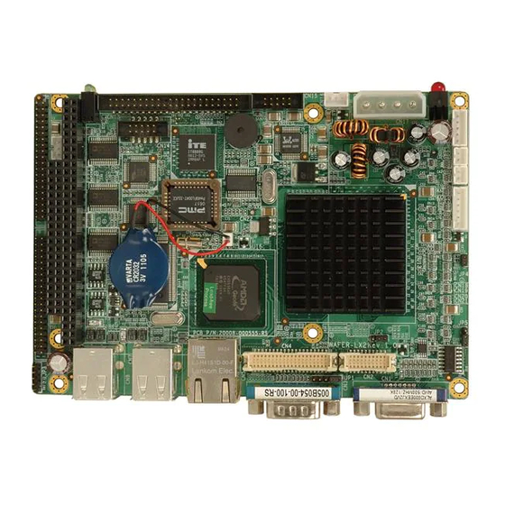
WAFER-LX2 3.5” Embedded SBC 1.1 WAFER-LX2 Overview Figure 1-1: WAFER-LX2 The 3.5” WAFER-LX2 AMD Geode LX800 low power single board computer (SBC) is fully equipped with advanced multi-mode I/Os. The WAFER-LX2 has eight serial ports and a PC/104 for expansion and increased connectivity. The WAFER-LX2 is designed for system manufacturers, integrators, and VARs that want performance, reliability, and quality at a reasonable price. -
Page 21: Wafer-Lx2 Features
WAFER-LX2 3.5” Embedded SBC Client crash prevention Central resource control Security protection 1.1.3 WAFER-LX2 Features Some of the WAFER-LX2 features are listed below: 3.5” form factor RoHS compliant AMD LX-800 processor installed Low power consumption (6 Watts) Two high performance 10/100 megabit Ethernet controllers on-board Two SATA channels with transfer rates up to 150MB/s on-board Four USB 2.0 devices on-board Integrated audio... -
Page 22: Wafer-Lx2 Overview
WAFER-LX2 3.5” Embedded SBC 1.2 WAFER-LX2 Overview NOTE: The LED light is optional customization. The LED Light must be pre-ordered ad does not come on the standard system. Figure 1-2: WAFER-LX2 Overview Page 4... -
Page 23: Wafer-Lx2 Connectors
WAFER-LX2 3.5” Embedded SBC Figure 1-3: WAFER-LX2 Solder Side Overview 1.2.1 WAFER-LX2 Connectors The WAFER-LX2 has the following connectors on-board: 1 x AT power connector 1 x ATX power function connector 1 x Audio connector 1 x Battery connector 1 x Compact Flash (CF) connector (solder side) 1 x External LED connector 1 x Fan connector 1 x General purpose input/output (GPIO) connector... -
Page 24: Technical Specifications
WAFER-LX2 3.5” Embedded SBC 1 x Reset button connector 2 x Serial port connectors 1 x Suspend power input connector 1 x TFT LCD LVDS interface connector 1 x TFT LCD TFT interface connector 1 x SO-DIMM socket The WAFER-LX2 has the following connectors on the board rear panel: 1 x Ethernet connectors 2 x Dual USB connector 1 x Serial port connector... -
Page 25: Table 1-1: Technical Specifications
WAFER-LX2 3.5” Embedded SBC 24-bit TTL or 18-bit single channel LVDS TTL/LVDS Supports one 1GB DDR 333/400 200-pin SO-DIMM Memory SDRAM module Award BIOS BIOS Compact Flash (CF) Audio AC'97 Codec Realtek ALC203 10/100 Base-T dual RTL8100C Eight RS-232 or Seven RS-232 and one RS-422/RS-485 Four USB 1.1 or USB 2.0 devices supported USB2.0... -
Page 26: Detailed Specifications
WAFER-LX2 3.5” Embedded SBC Chapter Detailed Specifications Page 8... -
Page 27: Overview
WAFER-LX2 3.5” Embedded SBC 2.1 Overview This chapter describes the specifications and on-board features of the WAFER-LX2 in detail. 2.2 Dimensions 2.2.1 Board Dimensions The dimensions of the board are listed below: Length: 146.06mm Width: 102mm Figure 2-1: WAFER-LX2 Dimensions (mm) 2.2.2 External Interface Panel Dimensions External peripheral interface connector panel dimensions are shown in Figure 2-2. -
Page 28: Data Flow
WAFER-LX2 3.5” Embedded SBC Figure 2-2: External Interface Panel Dimensions (mm) 2.3 Data Flow ® ® The WAFER-LX2 motherboard comes with an AMD Geode™ LX800 CPU and an AMD Geode™ CS5536 linked together by the GeodeLink™ Interface Unit. Figure 2-3 shows the data flow between the system chipset, the CPU and other components installed on the motherboard. -
Page 29: Cpu Support
WAFER-LX2 3.5” Embedded SBC Figure 2-3: Data Flow Block Diagram 2.4 CPU Support ® The WAFER-LX2 series motherboards all come with a preinstalled AMD Geode™ LX 800 500MHz CPU. ® 2.4.1 AMD Geode™ LX 800 500MHz Overview ® The specifications for the 500MHz AMD Geode™... -
Page 30: Amd Geode™ Lx 800 Memory Support
WAFER-LX2 3.5” Embedded SBC 64K I/64K D L1 cache and 128K L2 cache Split I/D cache/TLB (Translation Look-Aside Buffer) Integrated FPU that supports the Intel MMX® and AMD 3DNow!™ Technology instruction sets 9 GB/s internal GeodeLink™ Interface Unit (GLIU) Security Block 128-bit AES (CBC/ECB) True Random Number Generator ®... -
Page 31: Table 2-1: Geode Lx Graphics Features
WAFER-LX2 3.5” Embedded SBC Command buffer interface Hardware accelerated rotation BLTs Color depth conversion Paletized color Full 8x8 color pattern buffer Separate base addresses for all channels Monochrome inversion Table 2-1: Geode LX Graphics Features lists a complete list of Geode LX graphics features. -
Page 32: Amd Geode™ Lx 800 500Mhz Power Management
WAFER-LX2 3.5” Embedded SBC Variable Source Stride Variable Destination Stride Destination Write Bursting Selectable BLT Direction Vertical and Horizontal Yes (constant α, α/pix, or sep. α channel) Alpha BLT VGA Support Decodes VGA Register Pipeline Depth Unlimited Accelerated Rotation BLT 8, 16, 32 bpp Color Depth Conversion 5:6:5, 1:5:5:5, 4:4:4:4, 8:8:8:8... -
Page 33: Amd Geode™ Cs5536 Ata-6 Controller
WAFER-LX2 3.5” Embedded SBC PCI VSM (Virtual System Module) that makes the interface transparent to applications software and BIOS Programmable routing descriptors, use and activity monitors, and SSMI (Synchronous System Management Interrupt) ® 2.5.2 AMD Geode™ CS5536 ATA-6 Controller The single WAFER-LX2 IDE connector supports two ATA-6 HDDs. An ATA-6 (Ultra ®... - Page 34 WAFER-LX2 3.5” Embedded SBC The codec meets performance requirements for audio on PC99/2001 systems. Some of the codec features are listed below. Meets Microsoft WHQL/WLP 2.0 audio requirements 20-bit DAC and 18-bit ADC resolution 18-bit Stereo full-duplex CODEC with independent and variable sampling rate Complies with AC'97 2.3 specifications LINE/HP-OUT, MIC-IN and LINE-IN sensing 14.318MHz ->...
-
Page 35: Amd Geode™ Cs5536 Flash Interface
WAFER-LX2 3.5” Embedded SBC Supports 32K/44.1K/48KHz S/PDIF input Power support: Digital: 3.3V; Analog: 3.3V/5V Standard 48-Pin LQFP Package EAX™ 1.0 & 2.0 compatible Direct Sound 3D™ compatible A3D™ compatible I3DL2 compatible HRTF 3D Positional Audio Sensaura™ 3D Enhancement (optional) 10 Bands of Software Equalizer Voice Cancellation and Key Shifting in Kareoke mode AVRack®... -
Page 36: Amd Geode™ Cs5536 Real Time Clock
WAFER-LX2 3.5” Embedded SBC 16C550 UART with 16-byte FIFO buffer 115.2Kbps transmission rate ® 2.5.7 AMD Geode™ CS5536 Real Time Clock The system chipset has a battery backed up 256-byte real-time clock (RTC) with CMOS RAM. 2.5.8 BIOS The BIOS flash memory chip on the WAFER-LX2 has a licensed copy of AWARD BIOS loaded onto it. -
Page 37: 10/100M Ethernet
WAFER-LX2 3.5” Embedded SBC 32-bit, 66 MHz PCI bus operation Target support for fast back-to-back transactions Arbiter support for three external PCI bus masters Write gathering and write posting for in-bound write requests Virtual PCI header support Delayed transactions for in-bound read requests Zero wait state operation within a PCI burst Dynamic clock stop/start support for GLIU and PCI clock domains (this is not CLKRUN support) -
Page 38: Pci To Isa Bridge
WAFER-LX2 3.5” Embedded SBC Provides LED pins for network operation status indication 2.5/3.3V power supply with 5V tolerant I/Os 2.6.3 PCI to ISA Bridge An ITE IT8888G PCI to ISA bridge single function device connects the onboard WAFER-LX2 ISA bus PC/104 connector and the GPIO connector to the GeodeLink™ PCI bridge. -
Page 39: Operating Temperature And Temperature Control
WAFER-LX2 3.5” Embedded SBC CPU and board temperatures (by the corresponding embedded sensors) 2.7.2 Operating Temperature and Temperature Control The maximum and minimum operating temperatures for the WAFER-LX2 are listed below. Minimum Operating Temperature: 0ºC (32°F) Maximum Operating Temperature: 60°C (140°F) A cooling fan and heat sink must be installed on the CPU. -
Page 40: Unpacking
WAFER-LX2 3.5” Embedded SBC Chapter Unpacking Page 22... -
Page 41: Anti-Static Precautions
WAFER-LX2 3.5” Embedded SBC 3.1 Anti-static Precautions WARNING: Failure to take ESD precautions during the installation of the WAFER-LX2 may result in permanent damage to the WAFER-LX2 and severe injury to the user. Electrostatic discharge (ESD) can cause serious damage to electronic components, including the WAFER-LX2. -
Page 42: Unpacking Checklist
WAFER-LX2 3.5” Embedded SBC 3.3 Unpacking Checklist NOTE: If some of the components listed in the checklist below are missing, please do not proceed with the installation. Contact the IEI reseller or vendor you purchased the WAFER-LX2 from or contact an IEI sales representative directly. -
Page 43: Table 3-1: Package List Contents
WAFER-LX2 3.5” Embedded SBC IDE cable 4 COM Port Cable mini jumper Pack Quick Installation Guide Utility CD Table 3-1: Package List Contents Page 25... -
Page 44: Connector Pinouts
WAFER-LX2 3.5” Embedded SBC Chapter Connector Pinouts Page 26... -
Page 45: Peripheral Interface Connectors
WAFER-LX2 3.5” Embedded SBC 4.1 Peripheral Interface Connectors Section 4.1.2 shows peripheral interface connector locations. Section 4.1.2 lists all the peripheral interface connectors seen in Section 4.1.2. 4.1.1 WAFER-LX2 Layout Figure 4-1 shows the on-board peripheral connectors, rear panel peripheral connectors and on-board jumpers. -
Page 46: Peripheral Interface Connectors
WAFER-LX2 3.5” Embedded SBC Figure 4-2: Connector and Jumper Locations (Solder Side) 4.1.2 Peripheral Interface Connectors Table 4-1 shows a list of the peripheral interface connectors on the WAFER-LX2. Detailed descriptions of these connectors can be found below. Connector Type Label AT power connector 4-pin header... -
Page 47: External Interface Panel Connectors
WAFER-LX2 3.5” Embedded SBC GPIO connector 10-pin header CN14 IDE Interface connector 44-pin header CN13 Inverter power connector 5-pin header CN18 LED connector 6-pin header CN21 PC/104 power input connector 3-pin header CN10 PC/104 slot 104-pin slot CN12 Reset button connector 2-pin header CN20 Serial port connector (COM 2 –... -
Page 48: Internal Peripheral Connectors
WAFER-LX2 3.5” Embedded SBC 4.2 Internal Peripheral Connectors Internal peripheral connectors are found on the motherboard and are only accessible when the motherboard is outside of the chassis. This section has complete descriptions of all the internal, peripheral connectors on the WAFER-LX2. 4.2.1 AT Power Connector CN Label: CN17... -
Page 49: Atx Power Supply Enable Connector
WAFER-LX2 3.5” Embedded SBC PIN NO. DESCRIPTION +12V Table 4-3: AT Power Connector Pinouts 4.2.2 ATX Power Supply Enable Connector CN Label: CN16 CN Type: 3-pin wafer (1x3) CN Location: See Figure 4-4 CN Pinouts: See Table 4-4 The ATX power supply enable connector enables the WAFER-LX2 to be connected to an ATX power supply. -
Page 50: Audio Connector (10-Pin)
WAFER-LX2 3.5” Embedded SBC PIN NO. DESCRIPTION +5VSB PSON# Table 4-4: ATX Power Supply Enable Connector Pinouts 4.2.3 Audio Connector (10-pin) CN Label: CN15 CN Type: 10-pin header CN Location: See Figure 4-5 CN Pinouts: See Table 4-5 The 10-pin audio connector is connected to external audio devices including speakers an microphones for the input and output of audio signals to and from the system. -
Page 51: Backlight Inverter Connector
WAFER-LX2 3.5” Embedded SBC Line out L Line in L MIC in Table 4-5: Audio Connector Pinouts (10-pin) 4.2.4 Backlight Inverter Connector CN Label: CN18 CN Type: 5-pin wafer (1x5) CN Location: See Figure 4-6 CN Pinouts: See Table 4-6 The backlight inverter connector provides the backlight on the LCD display connected to the WAFER-LX2 with +12V of power. -
Page 52: Battery Connector
WAFER-LX2 3.5” Embedded SBC PIN NO. DESCRIPTION LCD_Adj GROUND +12V GROUND BACKLIGHT ENABLE Table 4-6: Panel Backlight Connector Pinouts 4.2.5 Battery Connector CN Label: CN22 CN Type: 2-pin wafer (1x2) CN Location: See Figure 4-7 CN Pinouts: See Table 4-7 The battery connector is connected to a backup battery. -
Page 53: Compact Flash Socket
WAFER-LX2 3.5” Embedded SBC PIN NO. DESCRIPTION Battery+ Ground Table 4-7: Battery Connector Pinouts 4.2.6 Compact Flash Socket CN Label: CN24 (solder side) CN Type: 50-pin header (2x25) CN Location: See Figure 4-8 CN Pinouts: See Table 4-8 A CF Type I or Type II memory card is inserted to the CF socket on the solder side of the WAFER-LX2. -
Page 54: Gpio Connector
WAFER-LX2 3.5” Embedded SBC PIDE_D8 PIDE_D9 PDASP# IDE_CABLEID PIDE_DRQ PIDE_ACK# PIDE_RST# PIDE_RDY VCC5 PIDE_INTRQ VCC5 PIDE_IOW# VCC5 PIDE_IOR# PIDE_D15 PIDE_CS#1 PIDE_13 PIDE_D14 PIDE_D11 PIDE_D12 Ground Ground PIDE_D2 PIDE_D0 PIDE_D1 PIDE_A1 PIDE_A0 Ground PIDE_A2 Ground Ground VCC5 Ground Ground Ground Ground Ground PIDE_CS#0 Ground... -
Page 55: Ide Connector(44-Pin)
WAFER-LX2 3.5” Embedded SBC The GPIO connector can be connected to external I/O control devices including sensors, lights, alarms and switches. Figure 4-9: GPIO Connector Pinout Locations PIN NO. DESCRIPTION PIN NO. DESCRIPTION Table 4-9: GPIO Connector Pinouts 4.2.8 IDE Connector(44-pin) CN13 CN Label: CN Type:... -
Page 56: Figure 4-10: Secondary Ide Device Connector Locations
WAFER-LX2 3.5” Embedded SBC Figure 4-10: Secondary IDE Device Connector Locations PIN NO. DESCRIPTION PIN NO. DESCRIPTION RESET# GROUND DATA 7 DATA 8 DATA 6 DATA 9 DATA 5 DATA 10 DATA 4 DATA 11 DATA 3 DATA 12 DATA 2 DATA 13 DATA 1 DATA 14... -
Page 57: Led Connector
WAFER-LX2 3.5” Embedded SBC GROUND Table 4-10: Secondary IDE Connector Pinouts 4.2.9 LED Connector CN Label: CN21 6-pin wafer (1x6) CN Type: CN Location: See Figure 4-11 CN Pinouts: See Table 4-11 The LED connector connects to an HDD indicator LED and a power LED on the system chassis to inform the user about HDD activity and the power on/off status of the system. -
Page 58: Pc/104 Slot
WAFER-LX2 3.5” Embedded SBC 4.2.10 PC/104 Slot CN Label: CN10 CN Type: 104-pin PC/104 slot CN Location: See Figure 4-12 CN Pinouts: See Table 4-12 The PC/104 slot enables a PC/104 compatible expansion module to be connected to the board. Figure 4-12: PC/104 Slot Location Page 40... - Page 59 WAFER-LX2 3.5” Embedded SBC Pin No. Column A Column B Column C Column D IOCHK- GROUND GROUND GROUND RSTDRV SBHE- MCS16- SA23 IOCS16- IRQ9 SA22 IRQ10 SA21 IRQ11 DREQ2 SA20 IRQ12 -12V SA19 IRQ15 ZWS- SA18 IRQ14 +12V SA17 DACK0- IOCHRDY GROUND MEMR-...
-
Page 60: Pc/104 Power Input Connector
WAFER-LX2 3.5” Embedded SBC ISA_OSC GROUND GROUND GROUND Table 4-12: PC/104 Slot Connector Pinouts 4.2.11 PC/104 Power Input Connector CN Label: CN12 CN Type: 3-pin wafer (1x3) CN Location: See Figure 4-13 CN Pinouts: See Table 4-13 The PC/104 power input connector provides power to the PC/104 expansion module installed on the PC/104 slot. -
Page 61: Power Button Connector
WAFER-LX2 3.5” Embedded SBC -12V Table 4-13: PC/104 Power Input Connector Pinouts 4.2.12 Power Button Connector CN Label: CN19 CN Type: 2-pin wafer (1x2) CN Location: See Figure 4-14 CN Pinouts: See Table 4-14 The power button connector is connected to a power switch on the system chassis to enable users to turn the system on and off. -
Page 62: Serial Port Connector (Com 2, Com 3 And Com 4)
WAFER-LX2 3.5” Embedded SBC CN Pinouts: See Table 4-15 The reset button connector is connected to a reset switch on the system chassis to enable users to reboot the system when the system is turned on. Figure 4-15: Reset Button Connector Locations PIN NO. -
Page 63: Figure 4-16: Com 2 To Com 4 Connector Pinout Locations
WAFER-LX2 3.5” Embedded SBC COM 2 is located on pin 1 to pin 20 RS-422/485: pin 1 to pin 7 RS-232: pin 11 to pin 20 COM 3 is located on pin 21 to pin 30 COM 4 is located on pin 31 to pin 40 Figure 4-16: COM 2 to COM 4 Connector Pinout Locations PIN NO. -
Page 64: Serial Port Connector (Com 5, Com 6, Com 7 And Com 8)
WAFER-LX2 3.5” Embedded SBC DTR3 DCD4 DSR4 RXD4 RTS4 TXD4 CTS4 DTR4 Table 4-16: COM 2 to COM 4 Connector Pinouts 4.2.15 Serial Port Connector (COM 5, COM 6, COM 7 and COM 8) CN Label: CN11 CN Type: 40-pin header (2x20) CN Location: See Figure 4-16 CN Pinouts:... -
Page 65: Figure 4-17: Com 5 To Com 8 Connector Pinout Locations
WAFER-LX2 3.5” Embedded SBC Figure 4-17: COM 5 to COM 8 Connector Pinout Locations PIN NO. DESCRIPTION PIN NO. DESCRIPTION DCD5 DSR5 RXD5 RTS5 TXD5 CTS5 DTR5 DCD6 DSR6 RXD6 RTS6 TXD6 CTS6 DTR6 DCD7 DSR7 RXD7 RTS7 TXD7 CTS7 DTR7 DCD8 DSR8... -
Page 66: Tft Lcd Lvds Connector
WAFER-LX2 3.5” Embedded SBC Table 4-17: COM 5 to COM 8 Connector Pinouts 4.2.16 TFT LCD LVDS Connector CN Label: 20-pin crimp (2x10) CN Type: CN Location: See Figure 4-18 CN Pinouts: See Table 4-18 The 20-pin TFT LCD LVDS can be connected to a TFT LCD screen directly. Figure 4-18: TFT LCD LVDS Connector Pinout Locations PIN NO. -
Page 67: Tft Lcd Ttl Connector
WAFER-LX2 3.5” Embedded SBC SDATA SCLK LCD_Vcc LCD_Vcc LCD_Vcc LCD_Vcc Table 4-18: TFT LCD LVDS Port Connector Pinouts 4.2.17 TFT LCD TTL Connector CN Label: CN Type: 40-pin crimp (2x20) CN Location: See Figure 4-19 CN Pinouts: See Table 4-19 The TFT LCD LVDS can be connected to a TFT LCD screen directly. -
Page 68: External Peripheral Interface Connectors
WAFER-LX2 3.5” Embedded SBC VSYNC LCD_EN HSYNC DISP_EN Table 4-19: TFT LCD TTL Port Connector Pinouts 4.3 External Peripheral Interface Connectors 4.3.1 External Peripheral Interface Connector Overview The WAFER-LX2 external peripheral interface connectors are listed below and shown in Figure 4-20: 1 x RJ-45 Ethernet connector 1 x Serial communications port 2 x USB combo port... -
Page 69: Ethernet Connector
WAFER-LX2 3.5” Embedded SBC Figure 4-20: WAFER-LX2 On-board External Interface Connectors 4.3.2 RJ-45 Ethernet Connector CN Label: CN Type: RJ-45 CN Location: See Figure 4-20 CN Pinouts: See Table 4-20 The RJ-45 Ethernet connector on the WAFER-LX2 provides connectivity to a 10/100 megabit Ethernet connection between the WAFER-LX2 and a Local Area Network (LAN) through a network hub. -
Page 70: Serial Port Connector (Com 1)
WAFER-LX2 3.5” Embedded SBC Figure 4-21: J7 Connector SPEED LED LINK LED Status Description Status Description GREEN ON: 100MB YELLOW ON: Linked OFF: 10MB Flashing: Activity Table 4-21: J7 Connector LEDs 4.3.3 Serial Port Connector (COM 1) CN Label: CN Type: DB-9 connector CN Location: See Figure 4-20... -
Page 71: Usb Combo Port
WAFER-LX2 3.5” Embedded SBC Figure 4-22: COM1 Pinout Locations 4.3.4 USB Combo Port CN Label: CN7 and CN8 CN Type: USB Combo port CN Location: See Figure 4-20 CN Pinouts: See Table 4-23 The two USB combo ports provide connectivity to USB devices. The USB port support both USB 1.1 and USB 2.0. -
Page 72: Figure 4-23: Vga Connector
WAFER-LX2 3.5” Embedded SBC CN Pinouts: See Figure 4-23 and Table 4-24 The standard 15-pin female DB15 VGA connector connects to a CRT or LCD monitor directly. DESCRIPTION DESCRIPTION DESCRIPTION GROUND GREEN GROUND DDCDAT BLUE GROUND HSYNC VSYNC GROUND GROUND DDCCLK Table 4-24: VGA Connector Pinouts Figure 4-23: VGA Connector... -
Page 73: Installation
WAFER-LX2 3.5” Embedded SBC Chapter Installation Page 55... -
Page 74: Anti-Static Precautions
WAFER-LX2 3.5” Embedded SBC 5.1 Anti-static Precautions WARNING: Failure to take ESD precautions during the installation of the WAFER-LX2 may result in permanent damage to the WAFER-LX2 and severe injury to the user. Electrostatic discharge (ESD) can cause serious damage to electronic components, including the WAFER-LX2. -
Page 75: Installation Considerations
WAFER-LX2 3.5” Embedded SBC 5.2 Installation Considerations NOTE: The following installation notices and installation considerations should be read and understood before the WAFER-LX2 is installed. All installation notices pertaining to the installation of the WAFER-LX2 should be strictly adhered to. Failing to adhere to these precautions may lead to severe damage of the WAFER-LX2 and injury to the person installing the motherboard. -
Page 76: Installation Checklist
WAFER-LX2 3.5” Embedded SBC When working with the WAFER-LX2, make sure that it is disconnected from all power supplies and that no electricity is being fed into the system. Before and during the installation of the WAFER-LX2 DO NOT: Remove any of the stickers on the PCB board. These stickers are required for warranty validation. -
Page 77: Sodimm Installation And Cf Card Installation
WAFER-LX2 3.5” Embedded SBC 5.3 SODIMM Installation and CF Card Installation 5.3.1 SODIMM Installation WARNING: Using an incorrectly specified SODIMM may cause permanent damage to the WAFER-LX2. Please make sure the purchased SODIMM complies with the memory specifications of the WAFER-LX2. SODIMM specifications compliant with the WAFER-LX2 are listed in Chapter 2. -
Page 78: Cf Card Installation
WAFER-LX2 3.5” Embedded SBC Step 3: Insert the SODIMM. Push the SODIMM chip into the socket at an angle. (See Figure 5-1) Step 4: Open the SODIMM socket arms. Gently pull the arms of the SODIMM socket out and push the rear of the SODIMM down. (See Figure 5-1) Step 5: Secure the SODIMM. -
Page 79: Jumper Settings
WAFER-LX2 3.5” Embedded SBC Figure 5-2: CF Card Installation 5.4 Jumper Settings NOTE: A jumper is a metal bridge that is used to close an electrical circuit. It consists of two metal pins and a small metal clip (often protected by a plastic cover) that slides over the pins to connect them. -
Page 80: At Power Select Jumper Settings
WAFER-LX2 3.5” Embedded SBC Description Label Type AT power select 2-pin header CF mode select 3-pin header COM 1 Pin 9 setting 5-pin header COM 2 function select 8-pin header LCD voltage select 3-pin header LCD clock select 3-pin header Table 5-1: Jumpers 5.4.1 AT Power Select Jumper Settings Jumper Label:... -
Page 81: Clear Cmos Jumper
WAFER-LX2 3.5” Embedded SBC Figure 5-3: AT Power Select Jumper Location 5.4.2 Clear CMOS Jumper Jumper Label: CN22 Jumper Type: 2-pin header Jumper Settings: See Table 5-3 Jumper Location: See Figure 5-4 If the WAFER-LX2 fails to boot due to improper BIOS settings, the CMOS can be cleared using the battery connector. -
Page 82: Cf Card Setup
WAFER-LX2 3.5” Embedded SBC AT Power Select Description Short Keep CMOS Setup Default Open Clear CMOS Setup Table 5-3: CN22 Clear CMOS Jumper Settings The location of the clear CMOS jumper is shown in Figure 5-4 below. Figure 5-4: CN22 Clear CMOS Jumper 5.4.3 CF Card Setup Jumper Label: Jumper Type:... -
Page 83: Com 1 Pin 9 Setting Jumper
WAFER-LX2 3.5” Embedded SBC CF Card Setup Description Short 1-2 Master Short 2-3 Slave Default Table 5-4: CF Card Setup Jumper Settings The CF Card Setup jumper location is shown in Figure 5-5. Figure 5-5: CF Card Setup Jumper Location 5.4.4 COM 1 Pin 9 Setting Jumper Jumper Label: Jumper Type:... -
Page 84: Com 2 Function Select Jumper
WAFER-LX2 3.5” Embedded SBC COM 1 RI Pin Description Short 1 – 2 COM 1 Pin 9 use RI Default Short 2 – 3 or COM 1 Pin 9 use +5V Short 3 – 4 Short 4 – 5 COM 1 Pin 9 use +12V Table 5-5: COM 1 Pin 9 Setting Jumper Settings The COM 1 Pin 9 Setting jumper location is shown in Figure 5-6 below. -
Page 85: Lcd Voltage Selection
WAFER-LX2 3.5” Embedded SBC COM 2 Function Select Description Short 1-2 RS-232 Default Short 3-4 and 7-8 RS-422 Short 5-6 and 7-8 RS-485 Table 5-6: COM 2 Function Select Jumper Settings The COM 2 Function Select jumper location is shown in Figure 5-9. Figure 5-7: COM 2 Function Select Jumper Location 5.4.6 LCD Voltage Selection WARNING:... -
Page 86: Lcd Clock Select Jumper
WAFER-LX2 3.5” Embedded SBC The LCD Voltage Selection jumper allows the LCD screen voltage to be set. The LCD Voltage Selection jumper settings are shown in Table 5-7. AT Power Select Description Short 1-2 +3.3V LVDS Default Short 2-3 +5V LVDS Table 5-7: LCD Voltage Selection Jumper Settings The LCD Voltage Selection jumper location. -
Page 87: Chassis Installation
WAFER-LX2 3.5” Embedded SBC LCD Clock Select Description Short 1-2 Normal LCD Clock Default Short 2-3 Inverted LCD Clock Table 5-8: LCD Clock Select Jumper Settings The LCD Clock Select jumper location is shown in Figure 5-9. Figure 5-9: LCD Clock Select Jumper Select Jumper Location 5.5 Chassis Installation 5.5.1 Airflow WARNING:... -
Page 88: Motherboard Installation
WAFER-LX2 3.5” Embedded SBC 5.5.2 Motherboard Installation To install the WAFER-LX2 motherboard into the chassis please refer to the reference material that came with the chassis. 5.6 Internal Peripheral Device Connections 5.6.1 Peripheral Device Cables The cables listed in Table 5-9 are shipped with the WAFER-LX2. Quantity Type ATA 66/100 flat cable... -
Page 89: Audio Kit Installation
WAFER-LX2 3.5” Embedded SBC Figure 5-10: IDE Cable Connection Step 3: Connect the cable to an IDE device. Connect the two connectors on the other side of the cable to one or two IDE devices. Make sure that pin 1 on the cable corresponds to pin 1 on the connectorStep 0: 5.6.3 Audio Kit Installation... -
Page 90: Four Serial Port Connector Cable
WAFER-LX2 3.5” Embedded SBC Step 2: Align pin 1. Align pin 1 on the onboard connector with pin 1 on the audio kit connector. Pin 1 on the audio kit connector is indicated with a white dot. See Figure 5-11. Figure 5-11: IDE Cable Connection Step 3: Connect the cable to an IDE device. -
Page 91: External Peripheral Interface Connection
WAFER-LX2 3.5” Embedded SBC connector is shown in Chapter 3. Step 2: Align the connectors. Correctly align pin 1 on the cable connector with pin 1 on the WAFER-LX2 serial port COM connector. See Figure 5-12. Step 3: Insert the cable connectors. - Page 92 WAFER-LX2 3.5” Embedded SBC Serial port devices USB devices VGA monitors RJ-45 Ethernet cable connectors To install these devices, connect the corresponding cable connector from the actual device to the corresponding WAFER-LX2 external peripheral interface connector making sure the pins are properly aligned. Page 74...
-
Page 93: Award Bios
WAFER-LX2 3.5” Embedded SBC Chapter AWARD BIOS Page 75... -
Page 94: Introduction
WAFER-LX2 3.5” Embedded SBC 6.1 Introduction A licensed copy of Phoenix Award BIOS is preprogrammed into the ROM BIOS. The BIOS setup program allows users to modify the basic system configuration. This chapter describes how to access the BIOS setup program and the configuration options that may be changed. -
Page 95: Getting Help
WAFER-LX2 3.5” Embedded SBC Item help Previous values for the page menu items Fail-safe defaults for the current page menu items Optimized defaults for the current page menu items Menu in BIOS Save changes and Exit BIOS Table 6-1: BIOS Navigation Keys 6.1.3 Getting Help When F1 is pressed a small help window describing the appropriate keys to use and the possible selections for the highlighted item appears. -
Page 96: Bios Menu 1: Award Bios Cmos Setup Utility
WAFER-LX2 3.5” Embedded SBC BIOS Menu 1: Award BIOS CMOS Setup Utility NOTE: The following sections will completely describe the menus listed below and the configuration options available to users. The following menu options are seen in BIOS Menu 1. Standard CMOS Features: Changes the basic system configuration. - Page 97 WAFER-LX2 3.5” Embedded SBC Load Fail-Safe Defaults Use the Load Fail-Safe Defaults option to load failsafe default values for each BIOS parameter in the setup menus. Press F6 for this operation on any page. Load Optimized Defaults Use the Load Optimized Defaults option to load optimal default values for each BIOS parameter in the setup menus.
-
Page 98: Standard Cmos Features
WAFER-LX2 3.5” Embedded SBC Exit Without Saving Use the Exit Without Saving option to exit the BIOS menus without saving any configuration changes. 6.2 Standard CMOS Features Use the Standard CMOS Features BIOS menu (BIOS Menu 2) to set basic BIOS configuration options. - Page 99 WAFER-LX2 3.5” Embedded SBC IDE Master and IDE Slave When entering setup, BIOS auto detects the presence of IDE devices. The Standard CMOS Features menu shows the status of the auto detected IDE devices. The following IDE devices are detected and shown in the Standard CMOS Features menu: IDE Primary Master IDE Primary Slave IDE Secondary Master...
-
Page 100: Ide Primary Master/Slave
WAFER-LX2 3.5” Embedded SBC or a disk error; it stops for all other errors. Base Memory: The Base Memory is NOT user configurable. The POST determines the amount of base (or conventional) memory installed in the system. The value of the base memory is typically 512K for systems with 512K memory installed, or 640K for systems with 640K or more memory installed. -
Page 101: Bios Menu 3: Ide Settings
WAFER-LX2 3.5” Embedded SBC BIOS Menu 3: IDE Settings IDE HDD Auto-Detection [Press Enter] Use the IDE HDD Auto-Detection option to enable BIOS to automatically detect the IDE settings. Select IDE HDD Auto-Detection and press E . BIOS automatically detects NTER the HDD type. - Page 102 WAFER-LX2 3.5” Embedded SBC inaccessible and any drives attached to it are undetected. Auto (Default) Setting this option allows the device to be automatically detected by the BIOS. Manual Selecting this option allows manual configuration of the device on the IDE channel in BIOS. Access Mode [Auto] The Access Mode option can only be configured if the BIOS configuration option is set to either Manual or Auto..
- Page 103 WAFER-LX2 3.5” Embedded SBC The Cylinder specification indicates how many cylinders (tracks) are on the HDD installed in the system. Head The Head specification indicates how many logical heads are on the HDD installed in the system. Precomp The Precomp specification indicates on what track the write precompensation begins. Landing Zone The Landing Zone specification indicates where the disk head will park itself after the system powers off.
-
Page 104: Advanced Bios Features
WAFER-LX2 3.5” Embedded SBC 6.3 Advanced BIOS Features Use the Advanced BIOS Features menu (BIOS Menu 4) to configure the CPU and peripheral device configuration options. BIOS Menu 4: Advanced BIOS Features Virus Warning [Disabled] NOTE: Many disk diagnostic programs can cause the above warning message to appear when the program attempts to access the boot sector table. - Page 105 WAFER-LX2 3.5” Embedded SBC BIOS halts the system and an error message appears. If necessary, an anti-virus program can then be run to locate and remove the virus before any damage is done. Enabled Activates automatically when the system boots up causing a warning message to appear when anything attempts to access the boot sector or HDD partition table.
- Page 106 WAFER-LX2 3.5” Embedded SBC Third Boot Device [Default: SCSI] Using the default values, the system first looks for a HDD to boot from. If it cannot find an HDD, it boots from a CD-ROM. If both The HDD and the CD-ROM are unavailable, the system boots from a SCSI drive.
- Page 107 WAFER-LX2 3.5” Embedded SBC Boot Up Numlock Status [On] Use the Boot Up Numlock Status option to specify the default state of the numeric keypad. The keys on the keypad are not activated. (Default) Activates the keys on the keypad. Typematic Rate Setting [Disabled] Use the Typematic Rate Setting configuration option to specify if only one character is allowed to appear on the screen if a key is continuously held down.
- Page 108 WAFER-LX2 3.5” Embedded SBC 30 characters per second Typematic Delay (Msec) [250] The Typematic Rate option can only be configured if the Typematic Rate Setting is enabled. Use the Typematic Delay option to specify the delay time between when a key is first pressed and when the acceleration begins.
- Page 109 WAFER-LX2 3.5” Embedded SBC OS Select For DRAM > 64MB [Non-OS2] Use the OS Select For DRAM > 64MB option to specify the operating system. Enabled Specifies the operating system used as OS/2. Disabled (Default) Select this option when not using the OS/2 operating system.
-
Page 110: Advanced Chipset Features
WAFER-LX2 3.5” Embedded SBC 6.4 Advanced Chipset Features Use the Advanced Chipset Features menu (BIOS Menu 5) to change chipset configuration options. BIOS Menu 5: Advanced Chipset Features CPU Frequency [500MHz] Use the CPU Frequency option to set the CPU frequency. The CPU Frequency options are: Auto 200MHz... - Page 111 WAFER-LX2 3.5” Embedded SBC Memory Frequency [333MHz] Use the Memory Frequency option to set the frequency of the installed DRAM modules. The Memory Frequency options are: 200MHz 266MHz 333MHz (Default) 400MHz Video Memory Size [8M] Use the Video Memory Size option to determine how much memory is allocated to the video graphics device.
-
Page 112: Flat Panel Configuration
WAFER-LX2 3.5” Embedded SBC OnBoard Audio [Enabled] Use the OnBoard Audio option to enable or disable the onboard codec. Disabled The onboard codec is disabled. Enabled (Default) The onboard codec is detected and enabled. 6.4.1 Flat Panel Configuration Use the Flat Panel Configuration menu (BIOS Menu 6) to set the configuration settings for the flat panel screen connected to the system. - Page 113 WAFER-LX2 3.5” Embedded SBC 800 x 600 (Default) 1024 x 768 1152 x 864 1280 x 1024 1600 x 1200 Data Bus Type [9 – 24 bits, 1 ppc] The Data Bus Type option can only be configured if the Flat Panel Type option is not set to Auto.
-
Page 114: Integrated Peripherals
WAFER-LX2 3.5” Embedded SBC High Low (Default) VSYNC Polarity Active [Low] The VGSYNC Polarity Active option can only be configured if the Flat Panel Type option is not set to Auto. Use the VGSYNC Polarity Active option to set the polarity of the VSYNC signal to the panel. -
Page 115: Bios Menu 7: Integrated Peripherals
WAFER-LX2 3.5” Embedded SBC BIOS Menu 7: Integrated Peripherals On-Chip IDE Channel 1 [Enabled] Use the On-Chip IDE Channel 1 option to specify if the system uses the integrated primary IDE channel or not. Disabled The primary IDE channel is not used. Enabled (Default) The primary IDE channel is used. - Page 116 WAFER-LX2 3.5” Embedded SBC Master Drive PIO Mode Slave Drive PIO Mode Auto (Default) The computer selects the correct mode. Mode 0 PIO mode 0 selected with a maximum transfer rate of 3.3MBps. PIO mode 1 selected with a maximum transfer rate of 5.2MBps. Mode 1 PIO mode 2 selected with a maximum transfer rate of 8.3MBps.
- Page 117 WAFER-LX2 3.5” Embedded SBC IDE DMA transfer access [Enabled] Use the IDE DMA transfer access option to enable or disable DMA support for IDE devices connected to the system. Disabled All IDE drive DMA transfers are disabled. The IDE drives use PIO mode transfers.
-
Page 118: It8888 Isa Decode Io
WAFER-LX2 3.5” Embedded SBC Onboard Serial Port 1 Onboard Serial Port 2 Onboard Serial Port 3 Onboard Serial Port 4 Onboard Serial Port 5 Onboard Serial Port 6 Onboard Serial Port 7 Onboard Serial Port 8 Serial Port N Use IRQ Use the Serial Port N Use IRQ option to select the IRQ for the N onboard serial port. -
Page 119: Bios Menu 8: It8888 Isa Decode Io
WAFER-LX2 3.5” Embedded SBC Use the IT8888 ISA Decode IO menu (BIOS Menu 8 to set the IO memory range for the onboard ISA. BIOS Menu 8: IT8888 ISA Decode IO The IT8888 ISA Decode IO menu has the following common options: Decode I/O Space N Decode I/O Speed N Decode I/O Addr. - Page 120 WAFER-LX2 3.5” Embedded SBC Enabled (Default) The Nth IO set is enabled and dedicated system resources are allocated to the Nth ISA bus. Decode IO Speed N [Fast Speed] Use the Decode IO Speed N option to specify the speed of the Nth ISA bus. The following options are available: Fast Speed Middle Speed...
-
Page 121: It8888 Isa Decode Memory
WAFER-LX2 3.5” Embedded SBC 6.5.2 IT8888 ISA Decode Memory NOTE: Five PCI-104 devices can be stacked onto the WAFER-LX2 motherboard. If these devices are stacked onto the board, the ISA memory should be enabled. If no PCI-104 devices are being used, disable all the memory allocations for these buses. - Page 122 WAFER-LX2 3.5” Embedded SBC Decode Memory Space N Decode Memory Speed N Decode Memory Addr. N [15:0] Decode Memory Size N Where N is an integer in the set [1, 2, 3, 4, 5] and represents a memory set for the PCI-104 devices that are attached to the system.
-
Page 123: Power Management Setup
WAFER-LX2 3.5” Embedded SBC Decode Memory Size N [xx] Use the Decode Memory Size N option to specify the memory size of the ISA bus. The following options are available: 16 KB 32 KB 64 KB 128 KB 256 KB 512 KB 1 MB 2 MB... -
Page 124: Pnp/Pci Configurations
WAFER-LX2 3.5” Embedded SBC AC Power Mode [ATX] Use the AC Power Mode to select either an AT or ATX power mode connected to the system. (Default) ATX power supply connected AT power supply connected Soft-Off by PWR-BTTN [Instant-Off] Use the Soft-Off by PWR-BTTN option to enabled the system to enter a very low-power-usage state when the power button is pressed. -
Page 125: Bios Menu 11: Pnp/Pci Configurations
WAFER-LX2 3.5” Embedded SBC BIOS Menu 11: PnP/PCI Configurations PNP OS Installed [No] The PNP OS Installed option determines whether the Plug and Play devices connected to the system are configured by the operating system or the BIOS. (Default) If the operating system does not meet the Plug and Play specifications, BIOS configures all the devices in the system. -
Page 126: Bios Menu 12: Irq Resources
WAFER-LX2 3.5” Embedded SBC Resources Controlled By [Auto (ESCD)] Use the Resources Controlled By option to either manually configure all the boot and plug and play devices, or allow BIOS to configure these devices automatically. If BIOS is allowed to configure the devices automatically IRQs, DMA and memory base address fields cannot be set manually. - Page 127 WAFER-LX2 3.5” Embedded SBC IRQ-4 assigned to IRQ-5 assigned to IRQ-7 assigned to IRQ-9 assigned to IRQ-10 assigned to IRQ-11 assigned to IRQ-12 assigned to The above options all have the following default options. PCI Device (Default) The IRQ is assigned to legacy ISA for devices compliant with the original PC AT bus specification, PCI/ISA PNP for devices compliant with the Plug and Play standard whether designed for PCI or ISA bus architecture.
-
Page 128: Bios Menu 13: Memory Resources
WAFER-LX2 3.5” Embedded SBC BIOS Menu 13: Memory Resources The menu has two configurable options: Reserved Memory Base Reserved Memory Length Reserved Memory Base [N/A] The Reserved Memory Base option specifies the base address for the peripheral device. The Reserved Memory Base options are: N/A (Default) C800 CC00... - Page 129 WAFER-LX2 3.5” Embedded SBC x Reserved Memory Length [8K] The Reserved Memory Length option can only be accessed if the Reserved Memory Base option is not set to N/A. The Reserved Memory Length specifies the amount of memory reserved for the peripheral device. The Reserved Memory Length options: 8K (Default) PCI/VGA Palette Snoop [Disabled] Use the PCI/VGA Palette Snoop option to enable the system to determine whether or not...
-
Page 130: Software Drivers
WAFER-LX2 3.5” Embedded SBC Chapter Software Drivers Page 112... -
Page 131: Available Software Drivers
WAFER-LX2 3.5” Embedded SBC 7.1 Available Software Drivers NOTE: The content of the CD may vary throughout the life cycle of the product and is subject to change without prior notice. You may visit the IEI website or contact technical support for the latest updates. There are five software drivers for the WAFER-LX2 motherboard installed in the subsystem: VGA Driver... -
Page 132: Figure 7-1: Amd Lx/Gx Cd Main Menu
WAFER-LX2 3.5” Embedded SBC Step 1: From the AMD LX/GX Driver CD main menu (Figure 7-1), click WAFER-LX2. Figure 7-1: AMD LX/GX CD Main Menu Step 2: A window appears listing the drivers available for installation (Figure 7-2). Page 114... -
Page 133: Vga Driver
WAFER-LX2 3.5” Embedded SBC Figure 7-2: AMD LX/GX CD Driver Menu Step 3: Select any item from the list to view more information on the driver installation, or select Manual to navigate to the WAFER-LX2 user manual. Step 0: The following sections fully describe the driver installation procedures for the WAFER-LX2 CPU card. -
Page 134: Figure 7-3: Access Windows Control Panel
WAFER-LX2 3.5” Embedded SBC Figure 7-3: Access Windows Control Panel Step 2: Double click the System icon (Figure 7-4). Page 116... -
Page 135: Figure 7-4: Double Click The System Icon
WAFER-LX2 3.5” Embedded SBC Figure 7-4: Double Click the System Icon Step 3: Double click the Device Manager tab (Figure 7-5). Page 117... -
Page 136: Figure 7-5: Double Click The Device Manager Tab
WAFER-LX2 3.5” Embedded SBC Figure 7-5: Double Click the Device Manager Tab Step 4: A list of system hardware devices appears (Figure 7-6). Page 118... -
Page 137: Figure 7-6: Device Manager List
WAFER-LX2 3.5” Embedded SBC Figure 7-6: Device Manager List Step 5: Expand the Display Adapters category (Figure 7-7). Right click the adapter and select Properties. NOTE: If the Display Adapters category is not available, navigate to X:\VGA\LX800\XP\VGA 2.01.05 (where X:\ is the system CD drive) and read the ReleaseNotes.txt file for further information on installing the VGA driver. -
Page 138: Figure 7-7: Expand The Display Adapters Category
WAFER-LX2 3.5” Embedded SBC Figure 7-7: Expand the Display Adapters Category Step 6: From the Driver tab of the Properties window, click Update Driver (Figure 7-8) or, click Reinstall Driver if Update Driver is not seen. Page 120... -
Page 139: Figure 7-8: Update Driver
WAFER-LX2 3.5” Embedded SBC Figure 7-8: Update Driver Step 7: The Upgrade Device Driver Wizard appears (Figure 7-9). Click N continue. Page 121... -
Page 140: Figure 7-9: Upgrade Device Driver Wizard
WAFER-LX2 3.5” Embedded SBC Figure 7-9: Upgrade Device Driver Wizard Step 8: The Install Hardware Device Driver screen appears (Figure 7-10). Select the Search for a suitable driver for my device radio button and click N continue. Page 122... -
Page 141: Figure 7-10: Search For Suitable Driver
WAFER-LX2 3.5” Embedded SBC Figure 7-10: Search for Suitable Driver Step 9: Select Specify a Location in the Locate Driver Files window (Figure 7-11). Click N to continue. Page 123... -
Page 142: Figure 7-11: Locate Driver Files
WAFER-LX2 3.5” Embedded SBC Figure 7-11: Locate Driver Files Step 10: Click Browse and navigate to the X:\AMD\LX800\XP\VGA 2.01.05 directory, where “X:” is the system CD drive (Figure 7-12). Page 124... -
Page 143: Audio Driver Installation
WAFER-LX2 3.5” Embedded SBC Figure 7-12: Location Browsing Window Step 11: Click OK to continue. Step 12: A driver files location menu window appears. Click N to continue. The driver is installed. Step 0: 7.3 Audio Driver Installation To install the audio driver please follow the steps below. Step 1: Open Windows Control Panel (Figure 7-13). -
Page 144: Figure 7-13: Access Windows Control Panel
WAFER-LX2 3.5” Embedded SBC Figure 7-13: Access Windows Control Panel Step 2: Double click the System icon (Figure 7-14). Page 126... -
Page 145: Figure 7-14: Double Click The System Icon
WAFER-LX2 3.5” Embedded SBC Figure 7-14: Double Click the System Icon Step 3: Double click the Device Manager tab (Figure 7-15). Page 127... -
Page 146: Figure 7-15: Double Click The Device Manager Tab
WAFER-LX2 3.5” Embedded SBC Figure 7-15: Double Click the Device Manager Tab Step 4: A list of system hardware devices appears (Figure 7-16). Page 128... -
Page 147: Figure 7-16: Device Manager List
WAFER-LX2 3.5” Embedded SBC Figure 7-16: Device Manager List Step 5: Double click the listed device that has question marks next to it. (This means Windows does not recognize the device). Step 6: The Device Driver Wizard appears (Figure 7-17). Click N to continue. -
Page 148: Figure 7-17: Search For Suitable Driver
WAFER-LX2 3.5” Embedded SBC Figure 7-17: Search for Suitable Driver Step 7: Select “Specify a Location” in the Locate Driver Files window (Figure 7-18). Click N to continue. Page 130... -
Page 149: Figure 7-18: Locate Driver Files
WAFER-LX2 3.5” Embedded SBC Figure 7-18: Locate Driver Files Step 8: Select “X:\ Audio\GeodeLX_XP_XPe_WDM_Audio_v2.03.00” directory in the location browsing window, where “X:\” is the system CD drive (Figure 7-19). Page 131... -
Page 150: Lan Driver
WAFER-LX2 3.5” Embedded SBC Figure 7-19: Location Browsing Window Step 9: Click OK to continue. A driver files location menu window appears. Select the LXWDMAu.inf file and click O to continue. The driver is installed. Step 0: 7.4 LAN Driver To install the LAN driver, please follow the steps below. -
Page 151: Figure 7-20: Locate The Setup Program Icon
WAFER-LX2 3.5” Embedded SBC Figure 7-20: Locate the Setup Program Icon Step 4: Double click the Setup program icon in Figure 7-20. Step 5: The Install Shield Wizard is prepared to guide the user through the rest of the process (Figure 7-21). Figure 7-21: Preparing Setup Screen Step 6: Once initialized, the Install Wizard welcome screen appears (Figure 7-22). -
Page 152: Figure 7-22: Install Wizard Welcome Screen
WAFER-LX2 3.5” Embedded SBC Figure 7-22: Install Wizard Welcome Screen Step 7: Click N to continue the installation or C to stop the installation. ANCEL Step 8: The Install Wizard starts to install the LAN driver. Step 9: Once the installation is complete, the InstallShield Wizard Complete screen appears (Figure 7-23). -
Page 153: Figure 7-23: Installing Screen
WAFER-LX2 3.5” Embedded SBC Figure 7-23: Installing Screen Step 10: Click F to complete the installation and exit the Install Shield Wizard. INISH Step 11: Once the installation process is complete, the computer may be restarted immediately or later. Select the preferred option and click F to complete the INISH installation process and exit the Install Shield Wizard (Figure 7-24). -
Page 154: Isa Driver
WAFER-LX2 3.5” Embedded SBC Figure 7-24: Restart the Computer 7.5 ISA Driver To install the IT8888 ISA Bridge driver please follow the steps below: Step 12: Open Windows Control Panel (Figure 7-25). Page 136... -
Page 155: Figure 7-25: Access Windows Control Panel
WAFER-LX2 3.5” Embedded SBC Figure 7-25: Access Windows Control Panel Step 13: Double click the System icon (Figure 7-26). Page 137... -
Page 156: Figure 7-26: Double Click The System Icon
WAFER-LX2 3.5” Embedded SBC Figure 7-26: Double Click the System Icon Step 14: Double click the Device Manager tab (Figure 7-27). Page 138... -
Page 157: Figure 7-27: Double Click The Device Manager Tab
WAFER-LX2 3.5” Embedded SBC Figure 7-27: Double Click the Device Manager Tab Step 15: A list of system hardware devices appears (Figure 7-28). Page 139... -
Page 158: Figure 7-28: Device Manager List
WAFER-LX2 3.5” Embedded SBC Figure 7-28: Device Manager List Step 16: Double click the listed device that has question marks next to it. (This means Windows does not recognize the device). Step 17: The Device Driver Wizard appears (Figure 7-29). Click N to continue. -
Page 159: Figure 7-29: Search For Suitable Driver
WAFER-LX2 3.5” Embedded SBC Figure 7-29: Search for Suitable Driver Step 18: Select “Specify a Location” in the Locate Driver Files window (Figure 7-30). Click N to continue. Page 141... -
Page 160: Figure 7-30: Locate Driver Files
WAFER-LX2 3.5” Embedded SBC Figure 7-30: Locate Driver Files Step 19: Select “X:\IT8888” directory in the location browsing window, where “X:\” is the system CD drive (Figure 7-31). Page 142... -
Page 161: Figure 7-31: Location Browsing Window
WAFER-LX2 3.5” Embedded SBC Figure 7-31: Location Browsing Window Step 20: Click OK to continue. A driver files location menu window appears. Select the ite.inf file and click O to continue. The driver is installed. Step 0: Page 143... -
Page 162: Abios Options
WAFER-LX2 3.5” Embedded SBC Appendix BIOS Options Page 144... - Page 163 WAFER-LX2 3.5” Embedded SBC Load Fail-Safe Defaults ..................79 Load Optimized Defaults..................79 Set Supervisor Password ..................79 Set User Password ....................79 Save & Exit Setup ....................79 Exit Without Saving ....................80 Date [Day mm:dd:yyyy] ..................80 Time [hh/mm/ss] ....................80 IDE Master and IDE Slave ..................81 Halt On [All, But Keyboard] ..................81 Base Memory: ......................82 Extended Memory ....................82...
- Page 164 WAFER-LX2 3.5” Embedded SBC Security Option [Setup]..................90 OS Select For DRAM > 64MB [Non-OS2].............91 Delay for HDD (secs) [3]..................91 HDD S.M.A.R.T Capability [Disabled] ..............91 Small Logo (EPA) Show [Disabled]..............91 CPU Frequency [500MHz] ..................92 Memory Frequency [333MHz] ................93 Video Memory Size [8M]..................93 Output Display [Panel &...
- Page 165 WAFER-LX2 3.5” Embedded SBC Decode Memory Speed N [Fast Speed] ............104 Decode Memory Address N [xx]................ 104 Decode Memory Size N [xx]................105 AC Power Mode [ATX]..................106 Soft-Off by PWR-BTTN [Instant-Off] ..............106 PNP OS Installed [No] ..................107 Reset Configuration Data [Disabled] ..............
-
Page 166: Bgpio Connection
WAFER-LX2 3.5” Embedded SBC Appendix GPIO Connection Page 148... -
Page 167: Gpio Settings And Default Values
WAFER-LX2 3.5” Embedded SBC B.1 GPIO Settings and Default Values B.1.1 GPIO Settings Two addresses (320h and 321h) on the LVC chipset are reserved to control the GPIO connector. Port 320h stores the data that is inputted to or outputted from the specified pin on the GPIO connector. -
Page 168: Assembly Language Samples
WAFER-LX2 3.5” Embedded SBC Bit 4 Bit 5 Bit 6 Bit 7 B.2 Assembly Language Samples B.2.1 GPIO Initialization Procedure The following instruction set initializes one pin on the GPIO connector. DX, 320h Moves 320h into the DX data register for one of the GPIO pins AL, XXh Moves the user defined output value XXh into the low bit... -
Page 169: General Purpose Input Procedure
WAFER-LX2 3.5” Embedded SBC Moves 320h into the DX data register for one of the DX, 320h GPIO pins AL, ZZh Moves the user defined output data ZZh into the low bit accumulator register AL DX, AL The ouput data in the low bit accumulator register AL is transmitted out from the address stored in the DX data register B.2.3 General Purpose Input Procedure... -
Page 170: Cwatchdog Timer
WAFER-LX2 3.5” Embedded SBC Appendix Watchdog Timer Page 152... - Page 171 WAFER-LX2 3.5” Embedded SBC NOTE: The following discussion applies to DOS environment. IEI support is contacted or the IEI website visited for specific drivers for more sophisticated operating systems, e.g., Windows and Linux. The Watchdog Timer is provided to ensure that standalone systems can always recover from catastrophic conditions that cause the CPU to crash.
- Page 172 WAFER-LX2 3.5” Embedded SBC NOTE: When exiting a program it is necessary to disable the Watchdog Timer, otherwise the system resets. Example program: ; INITIAL TIMER PERIOD COUNTER W_LOOP: AX, 6F02H ;setting the time-out value BL, 30 ;time-out value is 48 seconds ;...
-
Page 173: Daddress Mapping
WAFER-LX2 3.5” Embedded SBC Appendix Address Mapping Page 155... -
Page 174: I/O Address Mappings
WAFER-LX2 3.5” Embedded SBC D.1 I/O Address Mappings Table D-1: I/O Address Mappings Page 156... -
Page 175: Memory Address Mapping
WAFER-LX2 3.5” Embedded SBC D.2 Memory Address Mapping Table D-2: Memory Address Mapping Page 157... -
Page 176: Irq Mapping Table
WAFER-LX2 3.5” Embedded SBC D.3 IRQ Mapping Table Table D-3: IRQ Address Mapping Page 158... -
Page 177: Eexternal Ac'97 Audio Codec
WAFER-LX2 3.5” Embedded SBC Appendix External AC’97 Audio CODEC Page 159... -
Page 178: Introduction
WAFER-LX2 3.5” Embedded SBC E.1 Introduction The motherboard comes with an on-board Realtek ALC203 CODEC. Realtek ALC203 is a 16-bit, full duplex AC’97 Rev. 2.3 compatible audio CODECwith a sampling rate of 48KHz. E.1.1 Accessing the AC’97 CODEC The CODEC is accessed through a connector on the WAFER-LX2 motherboard. Connect the audio kit to the connector. - Page 179 WAFER-LX2 3.5” Embedded SBC To access the Sound Effects Manager, please do the following: Step 1: Install the audio CODEC driver. Step 2: Click either: The Sound Effect Manager icon in the Notification Area of the system task bar (see Figure E-2), or The Sound Effect Manager icon in the Control Panel (Figure E-3).
-
Page 180: Sound Effect Manager Configuration Options
WAFER-LX2 3.5” Embedded SBC NOTE: The Sound Effect Manager shown above is for the RealTek ALC655 audio CODEC. Different CODECs may have different sound manager appearances. The following section describes the different configuration options in the Sound Effect Manager. E.2.2 Sound Effect Manager Configuration Options The Sound Effects Manager enables configuration of the items listed below. - Page 181 WAFER-LX2 3.5” Embedded SBC NOTE: Not all RealTek Sound Effect Managers have all the above listed options. The Sound Effect Manager loaded onto the system may only have some of the options listed above. Below is a brief description of the available configuration options in the Sound Effects Manager.
- Page 182 WAFER-LX2 3.5” Embedded SBC Connector Sensing:- Realtek ALC655 detects if an audio device is plugged into the wrong connector. If an incorrect device is plugged in a warning message appears. HRTF Demo:- Adjust HRTF (Head Related Transfer Functions) 3D positional audio here before running 3D applications.
-
Page 183: Hazardous Materials Disclosure
WAFER-LX2 3.5” Embedded SBC Appendix Hazardous Materials Disclosure Page 165... -
Page 184: Hazardous Material Disclosure Table For Ipb Products Certified As Rohs Compliant Under 2002/95/Ec Without Mercury
WAFER-LX2 3.5” Embedded SBC F.1 Hazardous Material Disclosure Table for IPB Products Certified as RoHS Compliant Under 2002/95/EC Without Mercury The details provided in this appendix are to ensure that the product is compliant with the Peoples Republic of China (China) RoHS standards. The table below acknowledges the presences of small quantities of certain materials in the product, and is applicable to China RoHS only. - Page 185 WAFER-LX2 3.5” Embedded SBC Part Name Toxic or Hazardous Substances and Elements Lead Mercury Cadmium Hexavalent Polybrominated Polybrominated (Hg) (Cd) Chromium (Pb) Biphenyls Diphenyl Ethers (CR(VI)) (PBB) (PBDE) Housing Display Printed Circuit Board Metal Fasteners Cable Assembly Fan Assembly Power Supply Assemblies Battery This toxic or hazardous substance is contained in all of the homogeneous materials for the part is...
- Page 186 WAFER-LX2 3.5” Embedded SBC 此附件旨在确保本产品符合中国 RoHS 标准。以下表格标示此产品中某有毒物质的含量符 合中国 RoHS 标准规定的限量要求。 本产品上会附有”环境友好使用期限”的标签,此期限是估算这些物质”不会有泄漏或突变”的 年限。本产品可能包含有较短的环境友好使用期限的可替换元件,像是电池或灯管,这些 元件将会单独标示出来。 部件名称 有毒有害物质或元素 铅 汞 镉 六价铬 多溴联苯 多溴二苯醚 (Pb) (Hg) (Cd) (CR(VI)) (PBB) (PBDE) 壳体 显示 印刷电路板 金属螺帽 电缆组装 风扇组装 电力供应组装 电池 O: 表示该有毒有害物质在该部件所有物质材料中的含量均在 SJ/T11363-2006 标准规定的限量要求以下。 X: 表示该有毒有害物质至少在该部件的某一均质材料中的含量超出 SJ/T11363-2006 标准规定的限量要求。 Page 168...
Need help?
Do you have a question about the WAFER-LX2-800 and is the answer not in the manual?
Questions and answers