
Related Manuals for IEI Technology Wafer-GX


Summary of Contents for IEI Technology Wafer-GX
- Page 1 WAFER-GX Revision MODEL WAFER-LX2 AMD Geode LX800 Motherboard Revision Number Description Date of Issue Initial release November 2006 Page 1...
- Page 2 WAFER-GX WAFER-LX2 3.5” Embedded SBC PICOe-6612 5.25” CPU Card Copyright COPYRIGHT NOTICE The information in this document is subject to change without prior notice in order to improve reliability, design and function and does not represent a commitment on the part of the manufacturer.
-
Page 3: Table Of Contents
WAFER-GX Table of Contents INTRODUCTION..................... 1 1.1 WAFER-GX O .................... 2 VERVIEW 1.1.1 WAFER-GX Models ................... 2 1.1.2 WAFER-GX Applications ................... 2 1.1.3 WAFER-GX Benefits ..................2 1.1.4 WAFER-GX Features ..................3 1.2 WAFER-GX O .................... 4 VERVIEW 1.2.1 WAFER-GX Connectors..................5 1.2.2 Technical Specifications.................. - Page 4 2.17.2 Optional Accessory Items................21 CONNECTORS AND JUMPERS ................. 23 3.1 P ..............24 ERIPHERAL NTERFACE ONNECTORS 3.1.1 WAFER-GX Layout ..................24 3.1.2 Peripheral Interface Connectors ..............25 3.1.3 External Peripheral Interface Connectors............26 3.1.4 Onboard Jumpers..................... 27 3.2 I ..............27 NTERNAL...
- Page 5 4.2.1 Installation Notices ..................60 4.3 U ......................61 NPACKING 4.3.1 Unpacking Precautions..................61 4.3.2 Checklist......................62 4.4 WAFER-GX M ............62 OTHERBOARD NSTALLATION 4.4.1 DIMM Module Installation ................63 4.4.1.1 Purchasing the Memory Module............... 63 4.4.1.2 DIMM Module Installation............... 63 4.5 J...
- Page 6 WAFER-GX WAFER-LX2 3.5” Embedded SBC PICOe-6612 5.25” CPU Card 4.7.4 Keyboard and Mouse Connection..............78 AWARD BIOS SETUP ................... 79 5.1 I ......................80 NTRODUCTION 5.1.1 Starting Setup....................80 5.1.2 Using Setup ...................... 80 5.1.3 Getting Help..................... 81 5.1.4 Unable to Reboot After Configuration Changes..........81 5.1.5 Main BIOS Menu .....................
- Page 7 WAFER-GX B.3.1 Enable the DIO Input Function..............169 B.3.2 Enable the DIO Output Function ..............169 WATCHDOG TIMER ..................171 ADDRESS MAPPING..................175 D.1 A ...................... 176 DDRESS D.2 1 MB M ................. 176 EMORY DDRESS D.3 IRQ M .................... 177...
-
Page 8: List Of Figures
WAFER-LX2 3.5” Embedded SBC PICOe-6612 5.25” CPU Card List of Figures Figure 1-1: WAFER-GX Overview ................4 Figure 1-2: WAFER-GX Solder Side Overview ............5 Figure 2-1: WAFER-GX Dimensions (mm) ..............10 Figure 2-2: External Interface Panel Dimensions (mm)...........11 Figure 2-3: Data Flow Block Diagram................13 Figure 3-1: Connector and Jumper Locations ............24... - Page 9 WAFER-GX Figure 3-24: WAFER-GX On-board External Interface Connectors .......54 Figure 3-25: J7 Connector..................56 Figure 3-26: COM1 Pinout Locations ................57 Figure 3-27: VGA1 Connector ..................58 Figure 4-1: SO-DIMM Module Installation ..............64 Figure 4-2: Clear CMOS Connector ................66 Figure 4-3: AT/ATX Mode Select Jumper..............67 Figure 4-4: Serial Port Mode Select Jumper Pinout Locations ......68...
- Page 10 WAFER-GX WAFER-LX2 3.5” Embedded SBC PICOe-6612 5.25” CPU Card Figure 6-18: Locate Driver Files................143 Figure 6-19: Location Browsing Window............... 144 Figure 6-20: Locate the Setup Program Icon ............145 Figure 6-21: Preparing Setup Screen ..............145 Figure 6-22: Install Wizard Welcome Screen............146 Figure 6-23: Installing Screen .................
- Page 11 WAFER-GX List of Tables Table 1-1: WAFER-GX Model Specifications..............2 Table 1-2: Technical Specifications ................8 Table 2-1: Geode GX Graphics Features ..............15 Table 2-2: Power Consumption .................20 Table 3-1: Onboard Peripheral Connectors..............26 Table 3-2: Rear Panel Connectors................27 Table 3-3: Onboard Jumpers ..................27 Table 3-4: AT Power Connector Pinouts ..............28...
- Page 12 WAFER-GX WAFER-LX2 3.5” Embedded SBC PICOe-6612 5.25” CPU Card Table 3-24: J6 Connector Pinouts ................55 Table 3-25: J7 Connector Pinouts ................55 Table 3-26: J7 Connector LEDs .................56 Table 3-27: COM1 Pinouts..................57 Table 3-28: VGA1 Connector Pinouts ...............58 Table 4-1: Jumpers ....................65 Table 4-2: Clear CMOS Jumper Settings ..............66...
- Page 13 WAFER-GX BIOS Menus BIOS Menu 1: Award BIOS CMOS Setup Utility ............82 BIOS Menu 2: Standard CMOS Features ..............84 BIOS Menu 3: IDE Channel Master ................87 BIOS Menu 4: Advanced BIOS Features..............90 BIOS Menu 5: Advanced Chipset Features ..............98 BIOS Menu 6: Flat Panel Configuration ..............100 BIOS Menu 7: Integrated Peripherals..............
- Page 14 WAFER-GX WAFER-LX2 3.5” Embedded SBC PICOe-6612 5.25” CPU Card Glossary AC ’97 Audio Codec 97 Integrated Data Electronics ACPI Advanced Configuration and Input/Output Power Interface ICH4 I/O Controller Hub 4 Advanced Power Management L1 Cache Level 1 Cache ARMD ATAPI Removable Media Device...
-
Page 15: Introduction
WAFER-GX Chapter Introduction Page 1... -
Page 16: Wafer-Gx Overview
WAFER-GX 1.1 WAFER-GX Overview The 3.5” WAFER-GX AMD Geode GX 466 low power single board computer (SBC) is fully equipped with advanced multi-mode I/Os. The WAFER-GX is designed for system manufacturers, integrators, and VARs that want performance, reliability, and quality at a reasonable price. -
Page 17: Wafer-Gx Features
Reduced software costs Reduced maintenance costs Client crash prevention Central resource control Security protection 1.1.4 WAFER-GX Features Some of the WAFER-GX features are listed below: 3.5” form factor RoHS compliant Embedded AMD Geode GX 466 processor PC/104 expansion slot Dual-independent display functionality... -
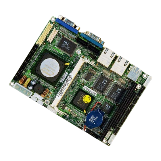
Page 18: Wafer-Gx Overview
WAFER-GX 1.2 WAFER-GX Overview Figure 1-1: WAFER-GX Overview Page 4... -
Page 19: Wafer-Gx Connectors
WAFER-GX Figure 1-2: WAFER-GX Solder Side Overview 1.2.1 WAFER-GX Connectors The WAFER-GX has the following connectors onboard: 1 x AT power input connector 1 x ATX power input connector 1 x Audio connector 1 x Battery connector 1 x CompactFlash (CF) connector (solder side) - Page 20 1 x Suspend power input connector 1 x TFT interface connector 1 x USB connector 1 x SO-DIMM socket The WAFER-GX has the following connectors on the board rear panel: 2 x Ethernet connectors 1 x PS/2 Keyboard/mouse connector 1 x USB connector...
-
Page 21: Technical Specifications
WAFER-GX 1.2.2 Technical Specifications WAFER-GX technical specifications are listed in Table 1-2. Detailed descriptions of each specification can be found in Chapter 2 Detailed Specifications. Specification WAFER-GX Form Factor 3.5” motherboard Geode™ GX 466 Front Side Bus (FSB) 333MHz ... -
Page 22: Table 1-2: Technical Specifications
WAFER-GX Software programmable 1-255 sec. by super I/O Digital I/O 8-bit digital I/O with 4 input and 4 output Fan connector One 3-pin for CPU Fan Expansion One PC/104 expansion slot Power +5V AT/ATX support Temperature 0ºC - 60ºC Humidity... -
Page 23: Detailed Specifications
WAFER-GX Chapter Detailed Specifications Page 9... -
Page 24: Overview
WAFER-GX 2.1 Overview This chapter describes the specifications and onboard features of the WAFER-GX in detail. 2.2 Board Dimensions 2.2.1 Board Dimensions The dimensions of the board are listed below: Length: 146.06mm Width: 102mm Figure 2-1: WAFER-GX Dimensions (mm) Page 10... -
Page 25: External Interface Panel Dimensions
2.2.2 External Interface Panel Dimensions External interface panel dimensions are shown in Figure 2-2. Figure 2-2: External Interface Panel Dimensions (mm) The WAFER-GX series motherboards all come with a preinstalled AMD Geode™ GX 466 333Mhz CPU. 2.2.3 Embedded AMD Geode™... -
Page 26: System Chipset
WAFER-GX Lower power I/O GeodeLink™ Interface Unit 2.3 System Chipset The WAFER-GX series motherboards all have a preinstalled AMD Geode™ CS5536 system chipset. The system chipset features are listed below. GeodeLink™ Interface Unit 64-bit, 66MHz operation PCI VSM (Virtual System Module) that makes the interface transparent to... -
Page 27: Data Flow
WAFER-GX General Purpose I/Os (GPIOs) 8 Multi-Function General Purpose Timers (MFGPTs) Real-Time Clock (RTC) with CMOS RAM Power Management Controller ACPI v2.0 compliant 2.4 Data Flow Figure 2-3 shows the data flow between the two onboard chipsets and other components installed on the motherboard and described in the following sections of this chapter. -
Page 28: Table 2-1: Geode Gx Graphics Features
WAFER-GX Incorporated BLT FIFOs to replace the cache based BLT buffers used in the GX1 processor. Improved bus protocols to increase bandwidth to the memory controller. The ability to throttle BLTs according to video timing and VGA hardware. Table 2-1: Geode GX Graphics Features lists a complete list of Geode GX graphics features. -
Page 29: Memory Support
Yes (constant α, α/pix, or sep. α channel) VGA Support Decodes VGA Register Table 2-1: Geode GX Graphics Features 2.6 Memory Support The WAFER-GX CPU has one 200-pin DDR SO-DIMM socket with the following specifications: Maximum RAM: 512MB DIMM Transfer Rates: 266MHz 2.7 PCI Bus Interface Support The PCI bridge on the WAFER-GX has the following features: 33MHz Revision 2.2 is implemented... -
Page 30: Features
Provides PCI clock run pin Provides LED pins for network operation status indication 2.5/3.3V power supply with 5V tolerant I/Os The WAFER-GX can support the following drive interfaces. 2 x SATA drives 2 x IDE devices 1 x FDD 1 x CF I or CF II card 2.8.3 SATA Drives... -
Page 31: Ide Hdd Interfaces
WAFER-GX The WAFER-GX supports two, first generation SATA drives with transfer rates of up to 150Mb/s 2.8.4 IDE HDD Interfaces The WAFER-GX system chipset IDE controller supports up to two HDDs with the following specifications: Supports PIO IDE transfers up to 16MB/s... -
Page 32: Usb Interfaces
The WAFER-GX has four USB interfaces, two internal (on one pin header connector) and two external. The USB interfaces support USB 2.0. 2.13 BIOS The WAFER-GX uses a licensed copy of AWARD BIOS. The features of the flash BIOS used are listed below: SMIBIOS (DMI) compliant... - Page 33 WAFER-GX designed for PC multimedia systems, including host/soft audio, and AMR/CNR based designs. The codec meets performance requirements for audio on PC99/2001 systems Single chip with high S/N ratio (>100 dB) Meets performance requirements for audio on PC2001 systems Meets Microsoft WHQL/WLP 2.0 audio requirements...
-
Page 34: Power Consumption
Voice Cancellation and Key Shifting in Kareoke mode AVRack® Media Player 2.16 Power Consumption Table 2-2 shows the power consumption parameters for the WAFER-GX when a 333MHz AMD Geode GX 400 is running with a 256MB DDR400 module. Voltage Current 1.15A... -
Page 35: Optional Accessory Items
WAFER-GX 1 x RS-232 cable 1 x RS-232/422/485 cable 2 x SATA cables 1 x SATA power cable 1 x Utility CD 1 x Quick Installation Guide 2.17.2 Optional Accessory Items The items shown in the list below are optional accessory items are purchased separately. - Page 36 WAFER-GX THIS PAGE IS INTENTIONALLY LEFT BLANK Page 22...
-
Page 37: Connectors And Jumpers
WAFER-GX Chapter Connectors and Jumpers Page 23... -
Page 38: Peripheral Interface Connectors
3.1 Peripheral Interface Connectors Section 3.1.1 shows peripheral interface connector locations. Section 3.1.2 lists all the peripheral interface connectors seen in Section 3.1.1. 3.1.1 WAFER-GX Layout Figure 3-1 shows the onboard peripheral connectors, external peripheral interface connectors and onboard jumpers. -
Page 39: Peripheral Interface Connectors
Figure 3-2: Connector and Jumper Locations (Solder Side) 3.1.2 Peripheral Interface Connectors Table 3-1 shows a list of the peripheral interface connectors on the WAFER-GX. Detailed descriptions of these connectors can be found in Section 3.2 on page 27. Connector... -
Page 40: External Peripheral Interface Connectors
8-pin header CN24 Table 3-1: Onboard Peripheral Connectors 3.1.3 External Peripheral Interface Connectors Table 3-2 lists the rear panel connectors on the WAFER-GX. Detailed descriptions of these connectors can be found in Section 3.3 on page 54. Connector Type Label... -
Page 41: Onboard Jumpers
Internal peripheral connectors are found on the motherboard and are only accessible when the motherboard is outside of the chassis. This section has complete descriptions of all the internal, peripheral connectors on the WAFER-GX. 3.2.1 AT Power Input Connector CN Label:... -
Page 42: Atx Power Connector
Table 3-4: AT Power Connector Pinouts 3.2.2 ATX Power Connector CN Label: CN11 CN Type: 3-pin wafer (1x2) CN Location: See Figure 3-4 CN Pinouts: See Table 3-5 The ATX power connector enables ATX power supply functionality on the WAFER-GX. Page 28... -
Page 43: Audio Connector
WAFER-GX Figure 3-4: ATX Power Connector Location PIN NO. DESCRIPTION VCC –5V GROUND VCC –12V Table 3-5: ATX Power Connector Pinouts 3.2.3 Audio Connector CN Label: CN Type: 10-pin header (2x5) CN Location: See Figure 3-5 CN Pinouts: See Table 3-6 The audio connector is connected to an onboard codec. -
Page 44: Compactflash Connector
WAFER-GX Figure 3-5: Audio Connector Location PIN NO. DESCRIPTION PIN NO. DESCRIPTION Line Out Right Line In Right Line Out Left Line In Left MIC 1 MIC 2 Table 3-6: Audio Connector Pinouts 3.2.4 CompactFlash Connector CN Label: CN32 (solder side) -
Page 45: Figure 3-7: Compactflash Connector Location
WAFER-GX Figure 3-6: CompactFlash Connector Location PIN NO. DESCRIPTION PIN NO. DESCRIPTION GROUND VCC-IN CHECK1 DATA 3 DATA 11 DATA 4 DATA 12 DATA 5 DATA 13 DATA 6 DATA 14 DATA 7 DATA 15 SDCS#1 SDCS#3 GROUND IOR# IOW#... -
Page 46: Digital Input/Output (Dio) Connector
WAFER-GX HDD_RESET IORDY SDREQ SDACK# HDD_ACTIVE# DATA 0 66DET DATA 1 DATA 8 DATA 2 DATA 9 DATA 10 VCC-IN CHECK2 GROUND Table 3-7: CompactFlash Connector Pinouts 3.2.5 Digital Input/Output (DIO) Connector CN Label: CN14 CN Type: 10-pin header (2x5) -
Page 47: Fan Connector
WAFER-GX Figure 3-7: DIO Connector Connector Locations PIN NO. DESCRIPTION PIN NO. DESCRIPTION Output 0 Output 1 Output 2 Output 3 Input 0 Input 1 Input 2 Input 3 Table 3-8: DIO Connector Connector Pinouts 3.2.6 Fan Connector CN Label:... -
Page 48: Ide Connector
WAFER-GX The cooling fan connector provides a 5V, 500mA current to a system cooling fan. The connector has a "rotation" pin to get rotation signals from fans and notify the system so the system BIOS can recognize the fan speed. Please note that only specified fans can issue the rotation signals. -
Page 49: Figure 3-10: Primary Ide Device Connector Locations
WAFER-GX CN Pinouts: See Table 3-10 One 40-pin IDE device connector on the WAFER-GX motherboard supports connectivity to two Ultra ATA 33 IDE devices with data transfer rates up to 100MB/s. Figure 3-9: Primary IDE Device Connector Locations PIN NO. -
Page 50: Inverter Power Connector
WAFER-GX IDE DRQ GROUND IOW# GROUND IOR# GROUND IDE CHRDY GROUND–DEFAULT IDE DACK GROUND INTERRUPT P66DET HDC CS0# HDC CS1# HDD ACTIVE# GROUND Table 3-10: Primary IDE Connector Pinouts 3.2.8 Inverter Power Connector CN Label: CN Type: 5-pin header (1x5) -
Page 51: Keyboard And Mouse Connector
WAFER-GX PIN NO. DESCRIPTION BL_ADJ VDD_EN Table 3-11: Inverter Power Connector Pinouts 3.2.9 Keyboard and Mouse Connector CN Label: CN17 CN Type: 6-pin wafer (1x6) CN Location: See Figure 3-11 CN Pinouts: See Table 3-12 The keyboard and mouse connector can be connected to a standard PS/2 cable or PS/2 Y-cable to add keyboard and mouse functionality to the system. -
Page 52: Led Connector
6-pin wafer (1x6) CN Location: See Figure 3-12 CN Pinouts: See Table 3-13 The LED connector is connected to LED power and HDD LED indicators locate on the chassis in which the WAFER-GX is installed. Figure 3-12: LED Connector Location Page 38... -
Page 53: Lcd Lvds Connector
WAFER-GX PIN NO. DESCRIPTION PWR LED+ PWR LED- HDD LED+ HDD LED- Table 3-13: LED Connector Pinouts 3.2.11 LCD LVDS Connector CN Label: CN29 CN Type: 20-pin crimp (2x10) CN Location: See Figure 3-13 CN Pinouts: See Figure 3-13 The TFT LCD LVDS can be connected to a TFT LCD screen directly. -
Page 54: Figure 3-14: Lcd Lvds Connector Locations
WAFER-GX Figure 3-13: LCD LVDS Connector Locations Page 40... -
Page 55: Lcd Ttl Connector
WAFER-GX DESCRIPTION DESCRIPTION LVDS_Y0+ LVDS_Y0- LVDS_Y1+ LVDS_Y1- LVDS_Y2+ LVDS_Y2- LVDS_CLK+ LVDS_CLK- LCD_VCC LCD_VCC LCD _VCC LCD _VCC Table 3-14: LCD LVDS Connector Pinouts 3.2.12 LCD TTL Connector CN Label: CN28 CN Type: 30-pin crimp (2x15) CN Location: CN Pinouts: The TFT LCD LVDS can be connected to a TFT LCD screen directly. -
Page 56: Figure 3-15: Lcd Ttl Connector Pinout Locations
WAFER-GX Figure 3-14: LCD TTL Connector Pinout Locations Page 42... -
Page 57: Parallel Port Connector
26-pin box header CN Location: See Figure 3-15 CN Pinouts: See Table 3-16 The WAFER-GX has one 26-pin header that can be connected to a parallel port connector interface or some other parallel port device such as a printer. Page 43... -
Page 58: Figure 3-16: Parallel Port Connector Location
WAFER-GX Figure 3-15: Parallel Port Connector Location PIN NO. DESCRIPTION PIN NO. DESCRIPTION STROBE# DATA 0 DATA 1 DATA 2 DATA 3 DATA 4 DATA 5 DATA 6 DATA 7 ACKNOWLEDGE BUSY PAPER EMPTY AUTO FORM FEED PRINTER SELECT ERROR#... -
Page 59: Pc/104 Slot
WAFER-GX 3.2.14 PC/104 Slot CN Label: CN10 CN Type: 104-pin PC/104 slot CN Location: See Figure 3-16 CN Pinouts: See Table 3-17 The PC/104 slot enables a PC/104 compatible expansion module to be connected to the board. Page 45... -
Page 60: Figure 3-17: Pc/104 Slot Location
WAFER-GX Figure 3-16: PC/104 Slot Location Pin No. Column A Column B Column C Column D Page 46... - Page 61 WAFER-GX IOCHK- GROUND GROUND GROUND RSTDRV SBHE- MCS16- SA23 IOCS16- IRQ9 SA22 IRQ10 SA21 IRQ11 DREQ2 SA20 IRQ12 -12V SA19 IRQ15 ZWS- SA18 IRQ14 +12V SA17 DACK0- IOCHRDY GROUND MEMR- DREQ0 SMEMW- MEMW- DACK5- SA19 SMEMR- DRREQ5 SA18 IOW- DACK6-...
-
Page 62: Power Switch Connector
WAFER-GX GROUND GROUND Table 3-17: PC/104 Slot Connector Pinouts 3.2.15 Power Switch Connector CN Label: CN13 CN Type: 2-pin wafer (1x2) CN Location: See Figure 3-17 CN Pinouts: See Table 3-18 The power switch connector is connected to the reset button on the external chassis. -
Page 63: Reset Button Connector
WAFER-GX PIN NO. DESCRIPTION PWRBTN# Table 3-18: Power Switch Connector Pinouts 3.2.16 Reset Button Connector CN Label: CN12 CN Type: 2-pin wafer (1x2) CN Location: See Figure 3-18 CN Pinouts: See Table 3-19 The reset button connector is connected to the reset button on the external chassis. -
Page 64: Rs-232/422/485 Serial Port Connectors
WAFER-GX Table 3-19: Reset Button Connector Pinouts 3.2.17 RS-232/422/485 Serial Port Connectors CN Label: CN16 CN Type: 14-pin box header (2x7) CN Location: See Figure 3-19 CN Pinouts: See Table 3-20 The serial port connector connects to an RS-232, RS-422 or RS-485 serial port devices. -
Page 65: Sata Drive Connectors
WAFER-GX GROUND GROUND TXD485+ TXD485# RXD485+ RXD485# Table 3-20: RS-232/422/485 Serial Port Connector Pinouts 3.2.18 SATA Drive Connectors CN Label: CN23 and CN25 CN Type: 7-pin SATA drive connectors CN Location: See Figure 3-20 CN Pinouts: See Table 3-21 The two SATA drive connectors are connected to two first generation SATA drives. First generation SATA drives transfer data at speeds as high as 150Mb/s. -
Page 66: Suspend Power Input
WAFER-GX PIN NO. DESCRIPTION Table 3-21: SATA Drive Connector Pinouts 3.2.19 Suspend Power Input CN Label: CN Type: 3-pin wafer (1x3) CN Location: See Figure 3-21 CN Pinouts: See Table 3-22 The suspend power connector is located next to the main AT power connector. -
Page 67: Internal Usb Connectors
WAFER-GX PIN NO. DESCRIPTION PS_ON# VCC 5VSB Table 3-22: Suspend Power Connector Pinouts 3.2.20 Internal USB Connectors CN Label: CN24 CN Type: 8-pin header (2x4) CN Location: See Figure 3-22 CN Pinouts: See Table 3-23 The two 2x4 USB pin connectors provide connectivity to four additional USB 2.0 ports. -
Page 68: External Interface Connectors
3.3 External Interface Connectors 3.3.1 External Interface Connector Overview Figure 3-23 shows the WAFER-GX motherboard external interface connectors. The WAFER-GX on-board external interface connectors are listed below and shown in Figure 3-23: 1 x USB combo port 2 x Ethernet connector... -
Page 69: Ethernet Connector
WAFER-GX The USB combo port provides connectivity to additional USB devices through an adapter cable. Various adapters may come with USB ports on a slot bracket or ports that can be attached to D-SUB openings on a chassis. USB devices connect directly to the USB connectors on the rear panel. -
Page 70: Serial Communications Com 1 And Com2 Connector
WAFER-GX Figure 3-24: J7 Connector The RJ-45 Ethernet connector has two status LEDs, one green and one yellow. The green LED indicates activity on the port and the yellow LED indicates the port is linked. SPEED LED LINK LED Status... -
Page 71: Vga Connector
WAFER-GX DESCRIPTION DESCRIPTION DCD1 DSR1 RTS1 CTS1 DTR1 Table 3-27: COM1 Pinouts Figure 3-25: COM1 Pinout Locations 3.3.5 VGA Connector CN Label: CN26 CN Type: See VGA Connector CN Location: See Figure 3-23 CN Pinouts: See Figure 3-26 and Table 3-28 The standard 15-pin female VGA connector connects to a CRT or LCD monitor. -
Page 72: Figure 3-27: Vga1 Connector
WAFER-GX VSYNC GROUND GROUND DDCCLK Table 3-28: VGA1 Connector Pinouts Figure 3-26: VGA1 Connector Page 58... -
Page 73: Installation And Configuration
WAFER-GX Chapter Installation and Configuration Page 59... -
Page 74: Anti-Static Precautions
4.1 Anti-static Precautions Electrostatic discharge (ESD) can cause serious damage to electronic components, including the WAFER-GX. (Dry climates are especially susceptible to ESD.) It is therefore critical that whenever the WAFER-GX (or any other electrical component) is handled, the following anti-static precautions are strictly adhered to. -
Page 75: Unpacking
4.3.1 Unpacking Precautions Before installing the WAFER-GX, unpack the motherboard. Some components on WAFER-GX are very sensitive to static electricity and can be damaged by a sudden rush of power. To protect it from being damaged, follow these precautions: The user should ground them self to remove any static charge before touching the WAFER-GX. -
Page 76: Checklist
1 x Utility CD 1 x Quick installation guide If one or more of these items are missing, please contact the reseller or vendor the WAFER-GX was purchased from and do not proceed any further with the installation. 4.4 WAFER-GX Motherboard Installation WARNING! Never run the motherboard without an appropriate heatsink and cooler that can be ordered from IEI Technology or purchased separately. -
Page 77: Dimm Module Installation
The SO-DIMM socket can support a memory chip with a maximum size of 512MB The SO-DIMM socket supports SDRAM DIMM speeds of 266MHz 4.4.1.2 DIMM Module Installation The WAFER-GX motherboard has two DDR SDRAM DIMM sockets. To install the DIMM modules, follow the instructions below. Step 1: Locate the SO-DIMM module connector. -
Page 78: Jumper Settings
OPEN a jumper means removing the plastic clip from a jumper. Before the WAFER-GX is installed in the system, the jumpers must be set in accordance with the desired configuration. The WAFER-GX motherboard has three on-board jumpers. Description... -
Page 79: Clear Cmos Jumper
Jumper Location: See Table 4-2 If the WAFER-GX fails to boot due to improper BIOS settings, use this connector to clear the CMOS data and reset the system BIOS information. To do this, disconnect CN7 and keep it disconnected for at least five seconds. After five seconds has elapsed, reinsert the connector. -
Page 80: Figure 4-2: Clear Cmos Connector
WAFER-GX Load Optimal Defaults Load Failsafe Defaults. After having done one of the above, save the changes and exit the CMOS Setup menu. DESCRIPTION Closed Keep CMOS Setup Open Clear CMOS Setup Table 4-2: Clear CMOS Jumper Settings The location of the clear CMOS connector is shown in Figure 4-2 below. -
Page 81: At Power Select Jumper Settings
WAFER-GX 4.5.2 AT Power Select Jumper Settings Jumper Label: Jumper Type: 2-pin header Jumper Settings: See Table 4-3 Jumper Location: See Figure 4-3 The AT/ATX Power Mode Select jumper specifies the systems power mode. Jumper settings are shown in Table 4-3. -
Page 82: Rs-422/485 Serial Port Select
WAFER-GX 4.5.3 RS-422/485 Serial Port Select Jumper Label: Jumper Type: 3-pin header Jumper Settings: See Table 4-4 Jumper Location: See Figure 4-4 This jumper configures the serial port connector as an RS-422 serial port or as an RS-485 serial port. The selection options are shown in Table 4-4. -
Page 83: Com 1/2 Port Ri And Voltage Select (Optional)
WAFER-GX 4.5.4 COM 1/2 Port RI and Voltage Select (OPTIONAL) Jumper Label: Jumper Type: 10-pin header Jumper Settings: See Table 4-5 Jumper Location: See Figure 4-5 This jumper configures the RI pin for both the COM 1 serial port and the COM 2 serial port. -
Page 84: Lcd Voltage Selection
Figure 4-5: COM 1/2 Port RI and Voltage Select Jumper Pinout Locations 4.5.5 LCD Voltage Selection WARNING Permanent damage to the screen and WAFER-GX may occur if the wrong voltage is selected with this jumper. Please refer to the user guide that cam with the monitor to select the correct voltage. -
Page 85: Crt/Lcd Mode Selection
WAFER-GX The JP4 jumper allows the LVDS screen voltage to be set. DESCRIPTION Short 1-2 (Default) +3.3V LVDS Short 2-3 +5V LVDS Table 4-6: LVDS Voltage Selection Jumper Settings The LVDS Voltage Selection jumper location is shown in Figure 4-6. -
Page 86: Chassis Installation
The LVDS Voltage Selection jumper location is shown in Figure 4-7. Figure 4-7: CRT/LCD Mode Selection Jumper Settings 4.6 Chassis Installation Cables provided by IEI that connect peripheral devices to the WAFER-GX are listed in Table 4-8. Cables not included in the kit must be separately purchased. Page 72... -
Page 87: Chassis Selection
Please visit the IEI website (www.ieiworld.com) or contact an IEI sales representative for more details. 4.6.2 Install the CompactFlash card To install the a CF card (Type 1 or Type 2) onto the WAFER-GX, please follow the steps below: Page 73... -
Page 88: Install The Rs-232/422/485 Cable
(Figure 4-8). Step 0: Figure 4-8: CompactFlash Card Installation 4.6.3 Install the RS-232/422/485 Cable The WAFER-GX is shipped with a RS-232/422/485 cable. To install the RS-232 cable please follow the steps below. Step 1: Locate the COM2 serial port connector. -
Page 89: Ide Disk Drive Connector
WAFER-GX 4.6.4 IDE Disk Drive Connector The WAFER-GX is shipped with an ATA 33 flat cable. The cable is connected to the WAFER-GX and to one or two IDE HDD. To connect an IDE HDD to the WAFER-GX, follow the instructions below. -
Page 90: Sata Drive Connection
0: 4.6.5 SATA Drive Connection The WAFER-GX four onboard 150Mb/s SATA drive connectors. The WAFER-GX is shipped with two SATA drive cables and one SATA drive power cable. To connect the SATA drives to the connectors, please follow the steps below. -
Page 91: Rear Panel Connectors
WAFER-GX of the SATA drive (Figure 4-11). Step 4: Connect the SATA power connector to the back of the SATA drive (Figure 4-11). Figure 4-11: SATA Drive Connection 4.7 Rear Panel Connectors 4.7.1 LCD Panel Connection The conventional CRT monitor connector, VGA1, is a 15-pin, female D-SUB connector. -
Page 92: Usb Connection
WAFER-GX 4.7.3 USB Connection The rear panel USB connectors provide easier and quicker access to external USB devices. The rear panel USB connector is a standard connector and can easily be connected to other USB devices. 4.7.4 Keyboard and Mouse Connection A PS/2 keyboard and a PS/2 mouse can be connected to the appropriate PS/2 connector on the rear panel. -
Page 93: Award Bios Setup
WAFER-GX Chapter AWARD BIOS Setup Page 79... -
Page 94: Introduction
WAFER-GX 5.1 Introduction A licensed copy of Phoenix Award BIOS is preprogrammed into the ROM BIOS. The BIOS setup program allows users to modify the basic system configuration. This chapter describes how to access the BIOS setup program and the configuration options that may be changed. -
Page 95: Getting Help
WAFER-GX General help, only for Status Page Setup Menu and Option Page Setup Menu Item help Previous values for the page menu items Fail-safe defaults for the current page menu items Optimized defaults for the current page menu items Menu in BIOS... -
Page 96: Bios Menu 1: Award Bios Cmos Setup Utility
WAFER-GX BIOS Menu 1: Award BIOS CMOS Setup Utility NOTE: The following sections will completely describe the menus listed below and the configuration options available to users. The following menu options are seen in BIOS Menu 1. Standard CMOS Features: Changes the basic system configuration. -
Page 97: Bios Menus
WAFER-GX Use the Load Fail-Safe Defaults option to load failsafe default values for each BIOS parameter in the setup menus. Press F6 for this operation on any page. Load Optimized Defaults Use the Load Optimized Defaults option to load optimal default values for each BIOS parameter in the setup menus. -
Page 98: Standard Cmos Features
WAFER-GX Use the Exit Without Saving option to exit the BIOS menus without saving any configuration changes. 5.2 Standard CMOS Features Use the Standard CMOS Features BIOS menu (BIOS Menu 2) to set basic BIOS configuration options. BIOS Menu 2: Standard CMOS Features... - Page 99 WAFER-GX IDE Primary Master IDE Primary Slave IDE Secondary Master IDE Secondary Slave IDE device configurations are changed or set in the IDE Configuration menu (BIOS Menu 3). If an IDE device is detected, and one of the above listed two BIOS configuration options is selected, the IDE configuration options shown in Section 5.2.1 appear.
-
Page 100: Ide Primary Master/Slave
WAFER-GX All Errors Whenever BIOS detects a non-fatal error the system is stopped and the user prompted. The system boot is not stopped for any errors No Errors that may be detected. All, But Keyboard (Default) The system boot does not stop for a keyboard error;... -
Page 101: Bios Menu 3: Ide Channel Master
WAFER-GX BIOS Menu 3: IDE Channel Master IDE HDD Auto-Detection [Press Enter] Use the IDE HDD Auto-Detection option to enable BIOS to automatically detect the IDE settings. Select IDE HDD Auto-Detection and press E . BIOS automatically detects NTER the HDD type. Do not set this option manually. - Page 102 WAFER-GX Channel 1 Master Channel 0 Slave None If no drives are connected to the IDE channel select this option. Once set, this channel becomes inaccessible and any drives attached to it are undetected. (Default) Setting this option allows the device to be automatically Auto detected by the BIOS.
-
Page 103: Advanced Bios Features
WAFER-GX The Capacity specification indicates the storage capacity of the HDD installed in the system. Cylinder The Cylinder specification indicates how many cylinders (tracks) are on the HDD installed in the system. Head The Head specification indicates how many logical heads are on the HDD installed in the system. -
Page 104: Bios Menu 4: Advanced Bios Features
WAFER-GX BIOS Menu 4: Advanced BIOS Features Virus Warning [Disabled] NOTE: Many disk diagnostic programs can cause the above warning message to Page 90... - Page 105 WAFER-GX appear when the program attempts to access the boot sector table. If you are running such a program, it is recommended that the virus protection function be disabled beforehand. Use the Virus Warning option to enable BIOS to monitor the boot sector and partition table of the HDD for any attempted modification.
- Page 106 WAFER-GX Use the BOOT From LAN Control option to enable the system to be booted from a remote system. Disabled (Default) The system cannot be booted from a remote system through the LAN. Enabled The system can be booted from a remote system through the LAN.
- Page 107 WAFER-GX HDD-1 HDD-2 HDD-3 ZIP100 USB-FDD USB-ZIP USB-CDROM USB-HDD Disabled Boot Other Device [Enabled] Use the Boot Other Device option to determine whether the system uses a second or third boot device if the first boot device is not found.
- Page 108 WAFER-GX Use the Boot Up Floppy Seek option to enable the BIOS to determine if the floppy disk drive installed has 40 or 80 tracks during the POST. 360K FDDs have 40 tracks while 760K, 1.2M and 1.44M FDDs all have 80 tracks.
- Page 109 WAFER-GX down, it begins to report that the key has been pressed repeatedly. This feature accelerates cursor movement with the arrow keys. Disabled (Default) Disables the typematic rate. Enabled Enables the typematic rate. Typematic Rate (Chars/sec) [6] The Typematic Rate option can only be configured if the Typematic Rate Setting is enabled.
- Page 110 WAFER-GX 1000 1000 milliseconds Security Option [Setup] Use the Security Option to limit access to both the system and Setup, or just Setup. Setup (Default) The system does not boot and access to Setup is denied if the correct password is not entered at the prompt.
-
Page 111: Advanced Chipset Features
WAFER-GX Enabled (Default) Video BIOS is copied to RAM. XXXXX-YYYYY Shadow [Disabled] Use the XXXXX-YYYYY Shadow option to write the contents of the ROM area XXXXX-YYYYY to the same address in the system RAM. (Default) Contents from ROM area XXXXX-YYYYY are not written Disabled to the RAM. -
Page 112: Bios Menu 5: Advanced Chipset Features
WAFER-GX BIOS Menu 5: Advanced Chipset Features CPU Frequency [200/133/33] Use the CPU Frequency option to set the CPU frequency. The CPU Frequency options are: 200/33/33 (Default) 333/222/33 Video Memory Size [8M] Use the Video Memory Size option to determine how much memory is allocated to the video graphics device. - Page 113 WAFER-GX Flat Panel Configuration [Press Enter] Use the Flat Panel Configuration option to open the Flat Panel Configuration menu. The Flat Panel Configuration options are shown in Section 5.4.1. OnBoard Audio [Enabled] Use the OnBoard Audio option to enable or disable the onboard codec.
-
Page 114: Flat Panel Configuration
WAFER-GX 5.4.1 Flat Panel Configuration Use the Flat Panel Configuration menu (BIOS Menu 6) to set the configuration settings for the flat panel screen connected to the system. BIOS Menu 6: Flat Panel Configuration Flat Panel Type [Auto] Use the Flat Panel Type option to specify the type of flat panel screen connected to the system. - Page 115 WAFER-GX The Resolution option can only be configured if the Flat Panel Type option is not set to Auto. Use the Resolution option to set the resolution of the flat panel screen connected to the system. The Resolution options are:...
- Page 116 WAFER-GX 60Hz (Default) 65Hz 70Hz 72Hz 75Hz 85Hz HSYNC Polarity [Low] The HSYNC Polarity option can only be configured if the Flat Panel Type option is not set to Auto. Use the HSYNC Polarity option to set the polarity of the HSYNC signal to the panel.
-
Page 117: Integrated Peripherals
WAFER-GX Active Only Free running (Default) 5.5 Integrated Peripherals Use the Integrated Peripherals menu (BIOS Menu 7) to change the configuration options for the attached peripheral devices. BIOS Menu 7: Integrated Peripherals Page 103... - Page 118 WAFER-GX On-Chip IDE Channel 0/1 [Enabled] Use the On-Chip IDE Channel 0/1 option to specify if the system uses the integrated primary IDE channel or not. Disabled The primary IDE channel is not used. Enabled (Default) The primary IDE channel is used.
- Page 119 WAFER-GX Auto (Default) The computer selects the correct UDMA. Disabled The UDMA for the HDD device is disabled. IDE DMA transfer access [Enabled] Use the IDE DMA transfer access option to enable or disable DMA support for IDE devices connected to the system.
- Page 120 WAFER-GX Use the Onboard FDC Controller option to enable or disable the onboard floppy controller. If the system is not connected to a floppy disk or uses an adapter for the FDD, this option can be disabled. Disabled The FDD controller is disabled.
- Page 121 WAFER-GX Normal (Default) RS-232C serial port IrDA Infrared port compliant with IrDA specification Amplitude shift keyed infrared port ASK IR x RxD, TxD Active [Hi,Lo] The RxD, TxD Active option can only be selected if the UART Mode Select option is set to IrDA mode or ASKIR mode.
- Page 122 WAFER-GX Use the Use IR Pins options to specify how the IR pins respond. The Use IR Pins options are: RxD2,TxD2 IR-Rx2Tx2 (Default) Onboard Parallel Port [378/IRQ7] Use the Onboard Parallel Port option to specify a logical LPT port address and corresponding interrupt for the physical parallel port.
- Page 123 WAFER-GX ECP+EPP The parallel port is compatible with both ECP and EPP devices. Normal x EPP Mode Select [EPP1.7] The EPP Mode Select option is only available if the Parallel Port Mode option is set to EPP mode. Use the EPP Mode Select option to select the parallel port mode standard for the parallel port.
-
Page 124: It8888 Isa Decode Io
WAFER-GX 5.5.1 IT8888 ISA Decode IO NOTE: Five PCI-104 devices can be stacked onto the WAFER-GX motherboard. If these devices are stacked onto the board, the ISA bus space should be enabled. If no PCI-104 devices are being used, disable all the buses. Disabling these buses frees up system resources that can be allocated to other system applications. -
Page 125: Bios Menu 8: It8888 Isa Decode Io
WAFER-GX BIOS Menu 8: IT8888 ISA Decode IO The IT8888 ISA Decode IO menu has the following common options: Decode I/O Space N Decode I/O Speed N Decode I/O Addr. N [15:0] Decode I/O Size N Page 111... - Page 126 WAFER-GX Where N is an integer in the set [1, 2, 3, 4, 5] and represents a set for the PCI-104 devices that are attached to the system. Decode IO Space N [Enabled] Use the Decode IO Space N option to allocate system resources to the ISA bridge and to enable the Nth PCI-104 to function correctly.
-
Page 127: It8888 Isa Decode Memory
5.5.2 IT8888 ISA Decode Memory NOTE: Five PCI-104 devices can be stacked onto the WAFER-GX motherboard. If these devices are stacked onto the board, the ISA memory should be enabled. If no PCI-104 devices are being used, disable all the memory allocations for these buses. -
Page 128: Bios Menu 9: It8888 Isa Decode Memory
WAFER-GX BIOS Menu 9: IT8888 ISA Decode Memory The IT8888 ISA Decode IO Memory menu has the following common options: Decode Memory Space N Decode Memory Speed N Decode Memory Addr. N [15:0] Decode Memory Size N Where N is an integer in the set [1, 2, 3, 4, 5] and represents a memory set for the PCI-104 devices that are attached to the system. -
Page 129: Power Management Setup
WAFER-GX Decode Memory Speed N [Fast Speed] Use the Decode Memory Speed N option to specify the memory speed of the ISA bus. The following options are available: Fast Speed Middle Speed Slow Speed Subtractive Speed Decode Memory Address N [xx] Use the Decode Memory Address N option to allocate an address to the memory of the ISA bus. -
Page 130: Bios Menu 10: Power Management Setup
WAFER-GX BIOS Menu 10: Power Management Setup ACPI Function [Disabled] The ACPI Function option is not user configurable. Power Management [ACPI] Use the Power Management option to set the power management type used by the system. All power management options are turned off. The only... - Page 131 WAFER-GX x Standby Mode [Disabled] The Standby Mode option can only be selected if the Power Management option is set to Legacy. The Standby Mode specifies the amount of time the system can be inactive before the system enters standby mode. The Standby Mode options are:...
-
Page 132: Power Management
WAFER-GX 1 Min 5 Min 10 Min 15 Min 30 Min 45 Min 60 Min 90 Min 120 Min Modem Use of IRQ [N/A] Use the Modem Use of IRQ to select the IRQ address for the system modem. The following IRQ addresses are available. -
Page 133: Bios Menu 11: Irq Wakeup Events
WAFER-GX RTC Alarm Date (Days) System Time After setting the alarm, the computer will turn itself on from a suspend state when the alarm goes off. IRQ Wakeup Events [Press Enter] To view the IRQ Wakeup Events options press E... -
Page 134: Pnp/Pci Configurations
WAFER-GX IRQ9 (IRQ2 Redir) IRQ10 (Reserved) IRQ11 (Reserved) IRQ12 (PS/2 Mouse) IRQ13 (Coprocessor) IRQ14 (Hard Disk) IRQ15 (Reserved) 5.7 PnP/PCI Configurations Use the PnP/PCI Configurations menu (BIOS Menu 12) to set the plug and play, and PCI options. BIOS Menu 12: PnP/PCI Configurations... - Page 135 WAFER-GX Set this option if the system is running Plug and Play aware operating systems. The operating system changes the interrupt, I/O, and DMA settings. Init. Display First [Onboard] Use the Init. Display First option to select the graphics controller the system uses as a primary boot device.
-
Page 136: Bios Menu 13: Irq Resources
WAFER-GX The IRQ Resources option (BIOS Menu 13) can only be selected if the Resources Controlled By option is set to Manual. BIOS Menu 13: IRQ Resources The IRQ Resources menu has the following options: IRQ-3 assigned to IRQ-4 assigned to... -
Page 137: Bios Menu 14: Memory Resources
WAFER-GX Reserved The IRQ is reserved by BIOS. x Memory Resources [Press Enter] The Memory Resources menu (BIOS Menu 14) can only be accessed if the Resources Controlled By option is set to Manual. Use Memory Resources to select a base address and the length for the memory area used by a peripheral that requires high memory. - Page 138 WAFER-GX D000 D400 D800 DC00 x Reserved Memory Length [8K] The Reserved Memory Length option can only be accessed if the Reserved Memory Base option is not set to N/A. The Reserved Memory Length specifies the amount of memory reserved for the peripheral device. The Reserved Memory Length options:...
-
Page 139: Pc Health Status
WAFER-GX Enabled (Default) An IRQ is assigned to the USB 5.8 PC Health Status The PC Health Status menu (BIOS Menu 15) has no user configurable options, but shows system operating parameters that are essential to the stable operation of the system. - Page 140 WAFER-GX CPU Warning Temperature [Disabled] Use the CPU Warning Temperature option to specify at what CPU temperature should the system issue a warning. The following configuration options are available: Disabled (Default) 50°C/122°F 53°C/127°F 56°C/133°F 60°C/140°F 63°C/145°F 66°C/151°F 70°C/158°F System Temperature...
-
Page 141: Software Drivers
WAFER-GX Chapter Software Drivers Page 127... -
Page 142: Available Software Drivers
The content of the CD may vary throughout the life cycle of the product and is subject to change without prior notice. You may visit the IEI website or contact technical support for the latest updates. There are five software drivers for the WAFER-GX motherboard installed in the subsystem: VGA Driver... -
Page 143: Figure 6-1: Amd Lx/Gx Cd Main Menu
WAFER-GX Figure 6-1: AMD LX/GX CD Main Menu Step 6: A window appears listing the drivers available for installation (Figure 6-2). Page 129... -
Page 144: Vga Driver
Select any item from the list to view more information on the driver installation, or select Manual to navigate to the WAFER-GX user manual. Step 0: The following sections fully describe the driver installation procedures for the WAFER-GX CPU card. 6.2 VGA Driver To install the VGA driver please follow the steps below. -
Page 145: Figure 6-3: Access Windows Control Panel
WAFER-GX Figure 6-3: Access Windows Control Panel Step 2: Double click the System icon (Figure 6-4). Page 131... -
Page 146: Figure 6-4: Double Click The System Icon
WAFER-GX Figure 6-4: Double Click the System Icon Step 3: Double click the Device Manager tab (Figure 6-5). Figure 6-5: Double Click the Device Manager Tab Step 4: A list of system hardware devices appears (Figure 6-6). Page 132... -
Page 147: Figure 6-6: Device Manager List
WAFER-GX Figure 6-6: Device Manager List Step 5: Expand the Display Adapters category (Figure 6-7). Right click the adapter and select Properties. NOTE: Display Adapters category available, navigate X:\VGA\LX800\XP\VGA 2.01.05 (where X:\ is the system CD drive) and read the ReleaseNotes.txt file for further information on installing the VGA driver. -
Page 148: Figure 6-7: Expand The Display Adapters Category
WAFER-GX Figure 6-7: Expand the Display Adapters Category Step 6: From the Driver tab of the Properties window, click Update Driver (Figure 6-8) or, click Reinstall Driver if Update Driver is not seen. Page 134... -
Page 149: Figure 6-8: Update Driver
WAFER-GX Figure 6-8: Update Driver Step 7: The Upgrade Device Driver Wizard appears (Figure 6-9). Click N continue. Page 135... -
Page 150: Figure 6-9: Upgrade Device Driver Wizard
WAFER-GX Figure 6-9: Upgrade Device Driver Wizard Step 8: The Install Hardware Device Driver screen appears (Figure 6-10). Select the Search for a suitable driver for my device radio button and click N continue. Page 136... -
Page 151: Figure 6-10: Search For Suitable Driver
WAFER-GX Figure 6-10: Search for Suitable Driver Step 9: Select Specify a Location in the Locate Driver Files window (Figure 6-11). Click N to continue. Page 137... -
Page 152: Figure 6-11: Locate Driver Files
WAFER-GX Figure 6-11: Locate Driver Files Step 10: Click Browse and navigate to the X:\AMD\LX800\XP\VGA 2.01.05 directory, where “X:” is the system CD drive (Figure 6-12). Figure 6-12: Location Browsing Window Step 11: Click OK to continue. Page 138... -
Page 153: Audio Driver Installation
WAFER-GX Step 12: A driver files location menu window appears. Click N to continue. The driver is installed. Step 0: 6.3 Audio Driver Installation To install the audio driver please follow the steps below. Step 1: Open Windows Control Panel (Figure 6-13). -
Page 154: Figure 6-14: Double Click The System Icon
WAFER-GX Figure 6-14: Double Click the System Icon Step 3: Double click the Device Manager tab (Figure 6-15). Figure 6-15: Double Click the Device Manager Tab Step 4: A list of system hardware devices appears (Figure 6-16). Page 140... -
Page 155: Figure 6-16: Device Manager List
WAFER-GX Figure 6-16: Device Manager List Step 5: Double click the listed device that has question marks next to it. (This means Windows does not recognize the device). Step 6: The Device Driver Wizard appears (Figure 6-17). Click N to continue. -
Page 156: Figure 6-17: Search For Suitable Driver
WAFER-GX Figure 6-17: Search for Suitable Driver Step 7: Select “Specify a Location” in the Locate Driver Files window (Figure 6-18). Click N to continue. Page 142... -
Page 157: Figure 6-18: Locate Driver Files
WAFER-GX Figure 6-18: Locate Driver Files Step 8: Select “X:\ Audio\GeodeLX_XP_XPe_WDM_Audio_v2.03.00” directory in the location browsing window, where “X:\” is the system CD drive (Figure 6-19). Page 143... -
Page 158: Lan Driver
WAFER-GX Figure 6-19: Location Browsing Window Step 9: Click OK to continue. A driver files location menu window appears. Select the LXWDMAu.inf file and click O to continue. The driver is installed. Step 0: 6.4 LAN Driver To install the LAN driver, please follow the steps below. -
Page 159: Figure 6-20: Locate The Setup Program Icon
WAFER-GX Figure 6-20: Locate the Setup Program Icon Step 4: Double click the Setup program icon in Figure 6-20. Step 5: The Install Shield Wizard is prepared to guide the user through the rest of the process (Figure 6-21). Figure 6-21: Preparing Setup Screen Step 6: Once initialized, the Install Wizard welcome screen appears (Figure 6-22). -
Page 160: Figure 6-22: Install Wizard Welcome Screen
WAFER-GX Figure 6-22: Install Wizard Welcome Screen Step 7: Click N to continue the installation or C to stop the installation. ANCEL Step 8: The Install Wizard starts to install the LAN driver. Step 9: Once the installation is complete, the InstallShield Wizard Complete screen appears (Figure 6-23). -
Page 161: Figure 6-23: Installing Screen
WAFER-GX Figure 6-23: Installing Screen Step 10: Click F to complete the installation and exit the Install Shield Wizard. INISH Step 11: Once the installation process is complete, the computer may be restarted immediately or later. Select the preferred option and click F... -
Page 162: Sata/Raid Driver
WAFER-GX Figure 6-24: Restart the Computer 6.5 SATA/RAID Driver To install the ALi SATA/RAID driver, please follow the steps below. Step 1: Click SATA from the AMD LX/GX CD Driver Menu to open a window to the X:\ALi_SATA_M5283 (where X:\ is the system CD drive) folder on the driver Step 2: Locate the Setup program icon (Figure 6-25). -
Page 163: Figure 6-25: Locate The Setup Program Icon
WAFER-GX Figure 6-25: Locate the Setup Program Icon Step 3: The Install Shield Wizard (Figure 6-26) is prepared to guide the user through the rest of the process. Figure 6-26: Preparing Setup Screen Step 4: Once initialized, the Install Wizard welcome screen appears (Figure 6-27). -
Page 164: Figure 6-27: Install Wizard Welcome Screen
WAFER-GX Figure 6-27: Install Wizard Welcome Screen Step 5: Click N to continue the installation or C to stop the installation. ANCEL Step 6: The Install Wizard starts to install the driver (Figure 6-28). Page 150... -
Page 165: Figure 6-28: Installing Screen
WAFER-GX Figure 6-28: Installing Screen Step 7: A “Digital Signal Not Found” screen appears (Figure 6-29). Click Y continue the installation process. Page 151... -
Page 166: Figure 6-29: Raid Driver Digital Signal
WAFER-GX Figure 6-29: RAID Driver Digital Signal Step 8: Once the installation is complete, the InstallShield Wizard Complete screen appears (Figure 6-30). Page 152... -
Page 167: Isa Driver
WAFER-GX Figure 6-30: InstallShield Wizard Complete Screen Step 9: Once the installation process is complete, the computer may be restarted immediately or later. Select the preferred option and click F to complete the INISH installation process and exit the Install Shield Wizard. -
Page 168: Figure 6-31: Access Windows Control Panel
WAFER-GX Figure 6-31: Access Windows Control Panel Step 2: Double click the System icon (Figure 6-32). Page 154... -
Page 169: Figure 6-32: Double Click The System Icon
WAFER-GX Figure 6-32: Double Click the System Icon Step 3: Double click the Device Manager tab (Figure 6-33). Page 155... -
Page 170: Figure 6-33: Double Click The Device Manager Tab
WAFER-GX Figure 6-33: Double Click the Device Manager Tab Step 4: A list of system hardware devices appears (Figure 6-34). Page 156... -
Page 171: Figure 6-34: Device Manager List
WAFER-GX Figure 6-34: Device Manager List Step 5: Double click the listed device that has question marks next to it. (This means Windows does not recognize the device). Step 6: The Device Driver Wizard appears (Figure 6-35). Click N to continue. -
Page 172: Figure 6-35: Search For Suitable Driver
WAFER-GX Figure 6-35: Search for Suitable Driver Step 7: Select “Specify a Location” in the Locate Driver Files window (Figure 6-36). Click N to continue. Page 158... -
Page 173: Figure 6-36: Locate Driver Files
WAFER-GX Figure 6-36: Locate Driver Files Step 8: Select “X:\IT8888” directory in the location browsing window, where “X:\” is the system CD drive (Figure 6-37). Page 159... -
Page 174: Figure 6-37: Location Browsing Window
WAFER-GX Figure 6-37: Location Browsing Window Step 9: Click OK to continue. A driver files location menu window appears. Select the ite.inf file and click O to continue. The driver is installed. Step 0: Page 160... -
Page 175: Abios Options
WAFER-GX Appendix BIOS Options Page 161... - Page 176 WAFER-GX Load Fail-Safe Defaults ..................82 Load Optimized Defaults..................83 Set Supervisor Password ..................83 Set User Password ....................83 Save & Exit Setup ....................83 Exit Without Saving ....................83 Date [Day mm:dd:yyyy] ..................84 Time [hh/mm/ss] ....................84 IDE Master and IDE Slave ..................84 Drive A/B [None] ....................85 Video ....................85...
- Page 177 WAFER-GX Swap Floppy Drive [Disabled] ................93 Boot Up Floppy Seek [Disabled] ................93 Boot Up Numlock Status [On] ................94 Gate A20 Option [Fast]..................94 Typematic Rate Setting [Disabled]...............94 Typematic Rate (Chars/sec) [6] ................95 Typematic Delay (Msec) [250]................95 Security Option [Setup]..................96 OS Select For DRAM > 64MB [Non-OS2].............96 Video BIOS Shadow [Enabled] ................96...
- Page 178 WAFER-GX IDE DMA transfer access [Enabled]..............105 IT8888 ISA Decode IO [Press Enter] ..............105 IT8888 ISA Decode Memory [Press Enter] ............105 IDE HDD Block Mode [Enabled] ................ 105 Onboard FDC Controller [Enabled]..............105 Onboard Serial Port 1 [3F8/IRQ4]..............106 Onboard Serial Port 2 [2F8/IRQ3]..............
- Page 179 WAFER-GX IRQ Wakeup Events [Press Enter] ..............119 PNP OS Installed [No] ..................120 Init. Display First [Onboard] ................121 Reset Configuration Data [Disabled] ..............121 Resources Controlled By [Auto (ESCD)]............121 x IRQ Resources [Press Enter]................121 x Memory Resources [Press Enter] ..............123 Reserved Memory Base [N/A]................
-
Page 180: This Page Is Intentionally Left Blank
WAFER-GX THIS PAGE IS INTENTIONALLY LEFT BLANK Page 166... -
Page 181: Bdio Connector
WAFER-GX Appendix DIO Connector Page 167... -
Page 182: Dio Interface Introduction
WAFER-GX B.1 DIO Interface Introduction The DIO connector on the WAFER-GX is interfaced to GIO ports on the Winbond W83627EHG Super I/O chipset. The DIO has both 4-bit digital inputs and 4-bit digital outputs. The digital inputs and digital outputs are generally control signals that control the on/off circuit of external devices or TTL devices. -
Page 183: Assembly Language Samples
WAFER-GX B.3 Assembly Language Samples B.3.1 Enable the DIO Input Function The BIOS interrupt call INT 15H controls the digital I/O. An assembly program to enable digital I/O input functions is listed below. Sets the digital port as input AX, 6F08H Initiates the INT 15H BIOS call B.3.2 Enable the DIO Output Function... - Page 184 WAFER-GX THIS PAGE IS INTENTIONALLY LEFT BLANK Page 170...
-
Page 185: Cwatchdog Timer
WAFER-GX Appendix Watchdog Timer Page 171... - Page 186 WAFER-GX NOTE: The following discussion applies to DOS environment. IEI support is contacted or the IEI website visited for specific drivers for more sophisticated operating systems, e.g., Windows and Linux. The Watchdog Timer is provided to ensure that standalone systems can always recover from catastrophic conditions that cause the CPU to crash.
- Page 187 WAFER-GX NOTE: When exiting a program it is necessary to disable the Watchdog Timer, otherwise the system resets. Example program: ; INITIAL TIMER PERIOD COUNTER W_LOOP: AX, 6F02H ;setting the time-out value BL, 30 ;time-out value is 48 seconds ; ADD THE APPLICATION PROGRAM HERE EXIT_AP, 1 ;is the application over?
- Page 188 WAFER-GX THIS PAGE IS INTENTIONALLY LEFT BLANK Page 174...
-
Page 189: Daddress Mapping
WAFER-GX Appendix Address Mapping Page 175... -
Page 190: Address Map
WAFER-GX D.1 Address Map I/O address Description Range 000-01F DMA Controller 020-021 Interrupt Controller 040-043 System time 060-06F Keyboard Controller 070-07F System CMOS/Real time Clock 080-09F DMA Controller 0A0-0A1 Interrupt Controller 0C0-0DF DMA Controller 0F0-0FF Numeric data processor 1F0-1F7 Primary IDE Channel... -
Page 191: Irq Mapping Table
WAFER-GX Table D-2: 1 MB Memory Address Map D.3 IRQ Mapping Table IRQ0 System Timer IRQ8 RTC clock IRQ1 Keyboard IRQ9 ACPI IRQ2 Available IRQ10 IRQ3 COM2 IRQ11 LAN/USB2.0/SATA IRQ4 COM1 IRQ12 PS/2 mouse IRQ5 SMBus Controller IRQ13 IRQ6 IRQ14... - Page 192 WAFER-GX THIS PAGE IS INTENTIONALLY LEFT BLANK Page 178...
-
Page 193: Eexternal Ac'97 Audio Codec
WAFER-GX Appendix External AC’97 Audio CODEC Page 179... -
Page 194: Introduction
16-bit, full duplex AC’97 Rev. 2.3 compatible audio CODECwith a sampling rate of 48KHz. E.1.1 Accessing the AC’97 CODEC The CODEC is accessed through a connector on the WAFER-GX motherboard. Connect the audio kit to the connector. E.1.2 Driver Installation The driver installation has been described in Chapter 6. -
Page 195: Sound Effect Configuration
WAFER-GX E.2 Sound Effect Configuration E.2.1 Accessing the Sound Effects Manager To access the Sound Effects Manager, please do the following: Step 1: Install the audio CODEC driver. Step 2: Click either: The Sound Effect Manager icon in the Notification Area of the system task bar (see Figure E-2), or The Sound Effect Manager icon in the Control Panel (Figure E-3). -
Page 196: Sound Effect Manager Configuration Options
WAFER-GX Figure E-4: Sound Effects Manager (ALC655) NOTE: The Sound Effect Manager shown in Error! Reference source not found. is for the RealTek ALC655 audio CODEC. Different CODECs may have different sound manager appearances. The following section describes the different configuration options in the Sound Effect Manager. - Page 197 WAFER-GX NOTE: The Karaoke Mode is configured in the Sound Effect menu. To access Karaoke configuration settings, click on the Sound Effect menu tab. Sound Effect Karaoke Mode Equalizer Speaker Configuration Speaker Test S/PDIF-In S/PDIF-Out Connector Sensing HRTF Demo Microphone Effect...
- Page 198 WAFER-GX The Key adjustment up or down arrow icons enables users to define a key that fits a certain vocal range. Equalizer Selection:- Preset equalizer settings enable easy audio range settings. Ten frequency bands can be configured. Speaker Configuration:- Multi-channel speaker settings are configured in this menu.
-
Page 199: Fali Raid
WAFER-GX Appendix Ali RAID Page 185... -
Page 200: Introduction
WAFER-GX F.1 Introduction The ALi M5283 SATA RAID chipset can control parallel ATA (PATA) and serial ATA (SATA) disks. The ALi controller supports PATA UDMA transfer mode up to mode 6 and SATA 1 disk drives. The ALi M5283 also has a cost-effective RAID functionality that can increase the data read/write speed and provide protection to data by distributing mirrored duplicates of data onto two disk drives (RAID 1). -
Page 201: Features And Benefits
WAFER-GX Do not accidentally disconnect the SATA drive cables. Carefully route the cables within the chassis to avoid system down time. F.2 Features and Benefits Supports RAID levels 0, 1, and JBOD Supports connectivity to two disk drives Supported Operating Systems include: Windows 98/Me, Windows 2000 and... - Page 202 WAFER-GX Step 7: Reboot the system. Reboot the system after saving and exiting the BIOS. Step 8: Press Ctrl-A. When the screen in FigureeF-1 appears press Ctrl-A to enter the ALi RAID BIOS setup program. FigureeF-1: Accessing ALi RAID BIOS Utility Step 9: Delete RAID settings and partitions.
-
Page 203: Raid Options
WAFER-GX FigureeF-2: RAID BIOS Setup Utility Step 10: Configure the RAID settings. Use the RAID BIOS Setup Utility in Error! Reference source not found. to configure the RAID array. Brief descriptions are given below. Step 11: Install the OS. After the RAID array has been configured (see below) install the OS. - Page 204 WAFER-GX destroyed during the RAID initialization process. If “used” drives are used to create a RAID array, make sure the data has been moved or backed up before creating a RAID array out of the disk drives. Step 1: Select “Create RAID 0 Striping for Performance”. Use the arrow keys to highlight Create RAID0 Striping for Performance and press E .
-
Page 205: Create Raid 1 Mirroring For Reliability
WAFER-GX F.4.2 Create RAID 1 Mirroring for Reliability WARNING! All data previously stored on the member drives of a RAID configuration is destroyed during the RAID initialization process. If “used” drives are used to create a RAID array, make sure the data has been moved or backed up before creating a RAID array out of the disk drives. -
Page 206: Create Jbod For Integrated Capacity
WAFER-GX Step 4: Name the array. Enter a nickname for the created array. Upper and lower case alphabetic, numeric, space, and underscore characters are all applicable for naming an array Step 5: View the array. A prompt appears to proceed with drive copy. The Source and Destination drives are indicated as “M”... - Page 207 WAFER-GX JBOD is defined as “Just a Bunch of Drives.” JBOD provides neither performance gains nor data redundancy. WARNING! All data previously stored on the member drives of a RAID configuration is destroyed during the RAID initialization process. If “used” drives are used to create a RAID array, make sure the data has been moved or backed up before creating a RAID array out of the disk drives.
-
Page 208: Stripe Size
WAFER-GX F.4.4 Stripe Size Changing the stripe size effects RAID 0 arrays. Configurable options are: 64K (default) Select a small stripe size if the I/Os to the hard drives are small and occur randomly. Choose a larger stripe size if the I/Os are mostly large and come in sequential orders, e.g., A/V playback and editing applications. -
Page 209: Rebuild Raid Array
WAFER-GX Step 1: Delete RAID Settings. Use the arrow keys to highlight Delete All RAID Setting & Partition and press E NTER Step 2: Confirm delete. The Data on RAID drives will be erased (Y/N) confirm box appears. Press Y. - Page 210 WAFER-GX THIS PAGE IS INTENTIONALLY LEFT BLANK Page 196...
-
Page 211: Index
WAFER-GX Index Page 197... - Page 212 WAFER-GX applications ........... 2 fan connector......5, 8, 25, 34 AT power connector ...... 27, 52 AT power input connector..... 5 ATA 33 IDE devices......35 Graphics Processor ....11, 13, 14 ATX power connector ......28 ATX power input connector....5 audio connector......
- Page 213 WAFER-GX power button connector....6, 26 SO-DIMM socket ....6, 15, 63, 64 power consumption......20 Suspend power input connector ..6, 26 power switch connector ...... 48 PS/2 Y-cable ........37 technical specifications ......7 TFT interface connector......6 reset button connector ....
Need help?
Do you have a question about the Wafer-GX and is the answer not in the manual?
Questions and answers